

Datasheet RQ5RW20AA-TR, RQ5RW20AB, RQ5RW20BA-TR, RQ5RW20BB, RQ5RW21AA-TR Datasheet (RICOH)
...Page 1

APPLICATION MANUAL
SMALL PACKAGE
VOLTAGE REGULATOR
RQ5RW SERIES
NO. EA-048-9803
ELECTRONIC DEVICES DIVISION
Page 2

NOTICE
1. The products and the product specifications described in this application manual are subject to change or
discontinuation of production without notice for reasons such as improvement. Therefore, before deciding to
use the products, please refer to Ricoh sales representatives for the latest information thereon.
2. This application manual may not be copied or otherwise reproduced in whole or in part without prior written
consent of Ricoh.
3. Please be sure to take any necessary formalities under relevant laws or regulations before exporting or
otherwise taking out of your country the products or the technical information described herein.
4. The technical information described in this application manual shows typical characteristics of and example
application circuits for the products. The release of such information is not to be construed as a warranty of or a
grant of license under Ricoh's or any third party's intellectual property rights or any other rights.
5. The products listed in this document are intended and designed for use as general electronic components in
standard applications (office equipment, computer equipment, measuring instruments, consumer electronic
products, amusement equipment etc.). Those customers intending to use a product in an application requiring
extreme quality and reliability, for example, in a highly specific application where the failure or misoperation of
the product could result in human injury or death (aircraft, spacevehicle, nuclear reactor control system, traffic
control system, automotive and transportation equipment, combustion equipment, safety devices, life support
system etc.) should first contact us.
6. We are making our continuous effort to improve the quality and reliability of our products, but semiconductor
products are likely to fail with certain probability. In order prevent any injury to persons or damages to property
resulting from such failure, customers should be careful enough to incorporate safety measures in their design,
such as redundancy feature, fire-containment feature and fail-safe feature. We do not assume any liability or
responsibility for any loss or damage arising from misuse or inappropriate use of the products.
7. Anti-radiation design is not implemented in the products described in this application manual.
8. Please contact Ricoh sales representatives should you have any questions or comments concerning the
products or the technical information.
June 1995
Page 3

RQ5RW SERIES
APPLICATION MANUAL
CONTENTS
OUTLINE
......................................................................................................
1
FEATURES
...................................................................................................
1
APPLICATIONS
.............................................................................................
1
BLOCK DIAGRAM
.........................................................................................
2
SELECTION GUIDE
.......................................................................................
2
PIN CONFIGURATION
...................................................................................
3
PIN DESCRIPTION
........................................................................................
3
ABSOLUTE MAXIMUM RATINGS
...................................................................
3
ELECTRICAL CHARACTERISTICS
................................................................
4
ELECTRICAL CHARACTERISTICS BY OUTPUT VOLTAGE
.............................
6
ELECTRICAL CHARACTERISTICS BY OUTPUT VOLTAGE
(common characteristics)
..........................................................................
7
OPERATION
..................................................................................................
7
TEST CIRCUITS
............................................................................................
8
TYPICAL CHARACTERISTICS
.......................................................................
9
1) Output Voltage vs. Output Current
......................................................................
9
2) Output Voltage vs. Input Voltage
.......................................................................
10
3) Dropout Voltage vs. Output Current
...................................................................
11
4) Output Voltage vs. Temperature
.......................................................................
11
5) Supply Current vs. Input Voltage
......................................................................
12
6) Supply Current vs. Temperature
.......................................................................
13
7) Dropout Voltage vs. Set Output Voltage
..............................................................
13
8) Line Transient Response
...............................................................................
14
9) Load Transient Response
..............................................................................
15
10) Ripple Rejection
.........................................................................................
16
Page 4

TYPICAL APPLICATION
..............................................................................
17
PACKAGE DIMENSION
................................................................................
17
TAPING SPECIFICATION
.............................................................................
18
Page 5

1
SMALL PACKA GE VOL TA GE REGULATOR
RQ5RW SERIES
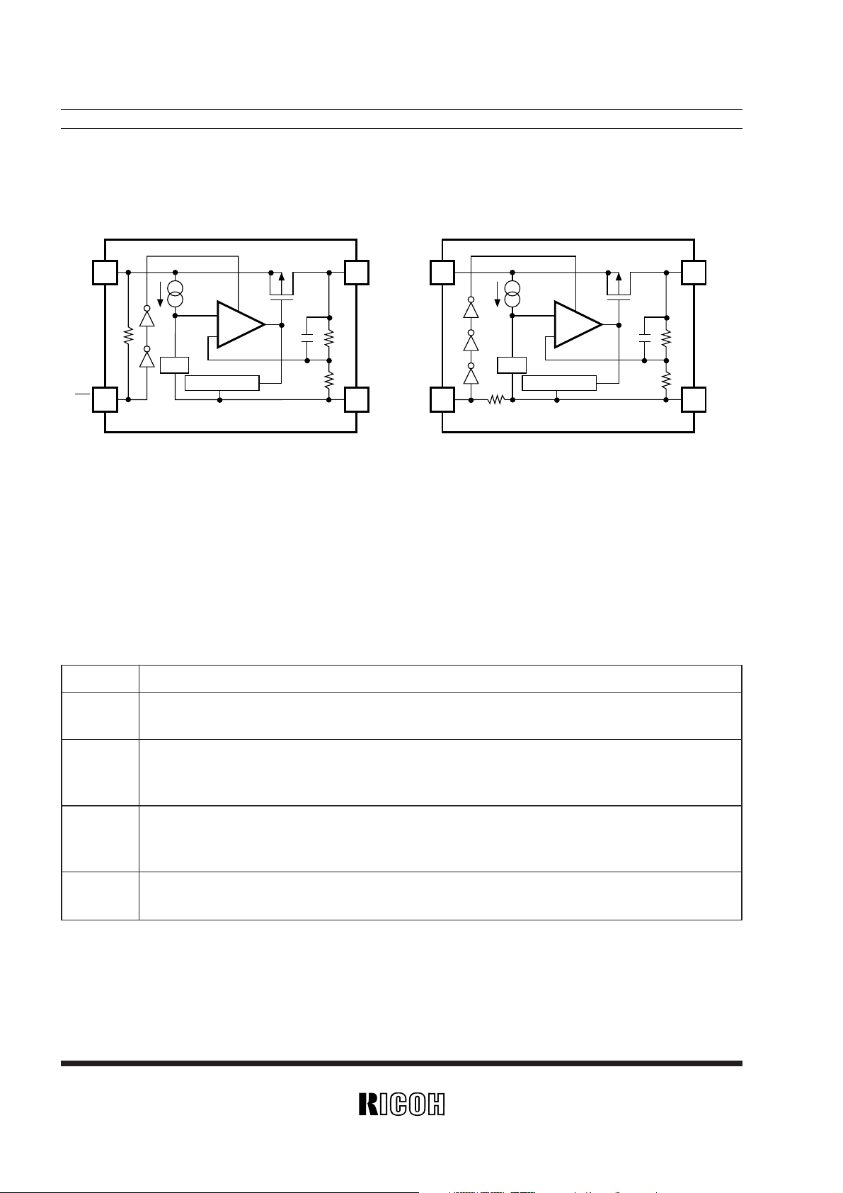
OUTLINE
The RQ5RW Series are voltage regulator ICs with high accuracy output voltage and ultra-low supply current developed by
CMOS process. Each of these ICs consists of a voltage reference unit, an error amplifier, resistors for setting output volt-
age and a current limit circuit.
The output voltage of these ICs is fixed with high accuracy.
Even if V
OUT is shorted to GND, the included current limit circuit protects the ICs from the destruction.
Furthermore, these ICs have a chip enable function, so that the supply current on standby can be minimized.
Since the package for these ICs are SC-82AB(Super Mini-mold)package, high density mounting of the ICs on boards is pos-
sible.
FEATURES
• Ultra-Low Supply Current
....................................
TYP. 1.5µA
• Standby Current
...................................................
TYP. 0.1µA
• Dropout Voltage
....................................................
TYP. 40mV (I
OUT=1mA, RQ5RW30A/B)
• Low Temperature-Drift Coefficient of
Output Voltage
......................................................
TYP. ±100ppm/˚C
• Excellent Line Regulation
....................................
TYP. 0.05%/V
• High Accuracy Output Voltage
...........................
±2.0%
• Ultra-Small Package
............................................
SC-82AB (Super Mini-mold)
• Built-in Current Llimit Circuits
APPLICATIONS
• Power source for battery-powered equipment.
• Power source for cameras, VCRs, camcorders, hand-held audio instruments and hand-held communication equipment.
• Precision voltage references.
Page 6
RQ5RW
2
BLOCK DIAGRAM
2
4
1
V
OUT
GND
V
DD
CE
Vref
3
Current Limit
2
4
1
V
OUT
GND
V
DD
CE
+
–
Vref
3
Current Limit
+
–
RQ5RW××A
RQ5RW
××B
SELECTION GUIDE
The output voltage, the active type, the packing type and the taping type for the ICs can be selected at the user's request.
The selection can be made by designating the part number as shown below:
RQ5RW
××××–××← Part Number
↑ ↑↑ ↑
a b c d
Code Contents
a
Setting Output Voltage (V
OUT) :
Stepwise setting with a step of 0.1V in the range of 2.0V to 6.0V is possible.
Designation of Chip enable Active Type :
b A : “L” active type
B : “H” active type
Designation of Packing Type :
c A : Taping
B : Antistatic bag (for Sample only)
d
Designation of Taping Type :
TR (refer to Taping Specifications)
}
}
Page 7
3
RQ5RW
PIN CONFIGURATION
1
2
4 3
(mark side)
• SC-82AB
PIN DESCRIPTION
Pin No. Symbol Pin Description
1 GND Ground Pin
2 VDD Input Pin
3 VOUT Output Pin
4 CE or CE Chip Enable Pin
ABSOLUTE MAXIMUM RATINGS
Symbol Item Rating Unit
VIN Input Voltage 9 V
VCE Input Voltage for CE/CE Pin –0.3 to VIN +0.3 V
VOUT Output Voltage –0.3 to V
IN +0.3 V
IOUT Output Current 150 mA
PD Power Dissipation 150 mW
Topt Operating Temperature –40 to +85 ˚C
Tstg Storage Temperature –55 to +125 ˚C
ABSOLUTE MAXIMUM RATINGS
Absolute Maximum ratings are threshold limit values that must not be exceeded even for an instant under
any conditions. Moreover, such values for any two items must not be reached simultaneously. Operation
above these absolute maximum ratings may cause degradation or permanent damage to the device. These
are stress ratings only and do not necessarily imply functional operation below these limits.
Page 8

RQ5RW
4
ELECTRICAL CHARACTERISTICS
Symbol Item Conditions MIN. TYP. MAX. Unit
VOUT Output Voltage
V
IN=5.0V
2.940 3.000 3.060 V
10µA≤IOUT≤10mA
I
OUT Output Current VIN=5.0V 50 mA
∆V
OUT
Load Regulation
V
IN=5.0V
40 60 mV
∆IOUT 1mA≤IOUT≤50mA
VDIF Dropout Voltage IOUT=1mA 40 60 mV
Iss Supply Current VIN=5.0V 1.5 3.0 µA
Istandby Standby Current VIN=5.0V, VCE=5.0V 0.1 1.0 µA
∆V
OUT
Line Regulation
I
OUT=1mA
0 0.05 0.20 %/V
∆VIN VOUT+0.5V≤VIN≤8V
VIN Input Voltage 8.0 V
∆V
OUT Output Voltage IOUT=10mA
±100 ppm/
˚C
∆Topt Temperature Coefficient –40˚C≤Topt≤85˚C
Ilim Short Current Limit 40 mA
RPU Pull up resistance for CE pin 1.5 4.0 12.0 MΩ
VCEH CE Input Voltage “H” 1.5 V
V
CEL CE Input Voltage “L” 0.25 V
Topt=25˚C
• RQ5RW30A
Page 9

5
RQ5RW
• RQ5RW30B
Symbol Item Conditions MIN. TYP. MAX. Unit
VOUT Output Voltage
V
IN=5.0V
2.940 3.000 3.060 V
10µA≤IOUT≤10mA
IOUT Output Current VIN=5.0V 50 mA
∆V
OUT
Load Regulation
V
IN=5.0V
40 60 mV
∆IOUT 1mA≤IOUT≤50mA
VDIF Dropout Voltage IOUT=1mA 40 60 mV
Iss Supply Current VIN=5.0V 1.5 3.0 µA
Istandby Standby Current VIN=5.0V, VCE=GND 0.1 1.0 µA
∆V
OUT
Line Regulation
I
OUT=1mA
0 0.05 0.20 %/V
∆VIN VOUT
+0.5V≤VIN≤8V
VIN Input Voltage 8.0 V
∆V
OUT Output Voltage IOUT=1mA
±100 ppm/
˚C
∆Topt Temperature Coefficient –40˚C≤Topt≤85˚C
Ilim Short Current Limit 40 mA
RPD Pull down resistance for CE pin 1.5 4.0 12.0 MΩ
VCEH CE Input Voltage “H” 1.5 V
V
CEL CE Input Voltage “L” 0.25 V
Topt=25˚C
Page 10

RQ5RW
6
ELECTRICAL CHARACTERISTICS BY OUTPUT VOLTAGE
VIN–
60 90
V
OUT
=2.0V
35 30 45
1mA
≤
50 75
I
OUT
≤35mA
40 60
V
IN–
VOUT
=2.0V
35 55
50 40 60
1mA
≤
IOUT
≤50mA
30 45
IOUT
=1mA
V
IN–
VOUT
=2.0V
65 50 70
1mA
≤
IOUT
≤65mA
25 40
V
IN–
VOUT
=2.0V
80 60 90
1mA
≤
IOUT
≤80mA
RQ5RW20 1.960 2.000 2.040
RQ5RW21 2.058 2.100 2.142
RQ5RW22 2.156 2.200 2.244
RQ5RW23 2.254 2.300 2.346
RQ5RW24 2.352 2.400 2.448
RQ5RW25 2.450 2.500 2.550
RQ5RW26 2.548 2.600 2.652
RQ5RW27 2.646 2.700 2.754
RQ5RW28 2.744 2.800 2.856
RQ5RW29 2.842 2.900 2.958
RQ5RW30 2.940 3.000 3.060
RQ5RW31 3.038 3.100 3.162
RQ5RW32 3.136 3.200 3.264
RQ5RW33 3.234 3.300 3.366
RQ5RW34 3.332 3.400 3.468
RQ5RW35 3.430 3.500 3.570
RQ5RW36 3.528 3.600 3.672
RQ5RW37 3.626 3.700 3.774
RQ5RW38 3.724 3.800 3.876
RQ5RW39 3.822 3.900 3.978
RQ5RW40 3.920 4.000 4.080
RQ5RW41 4.018 4.100 4.182
RQ5RW42 4.116 4.200 4.284
RQ5RW43 4.214 4.300 4.386
RQ5RW44 4.312 4.400 4.488
RQ5RW45 4.410 4.500 4.590
RQ5RW46 4.508 4.600 4.692
RQ5RW47 4.606 4.700 4.794
RQ5RW48 4.704 4.800 4.896
RQ5RW49 4.802 4.900 4.998
RQ5RW50 4.900 5.000 5.100
RQ5RW51 4.998 5.100 5.202
RQ5RW52 5.096 5.200 5.304
RQ5RW53 5.194 5.300 5.406
RQ5RW54 5.292 5.400 5.508
RQ5RW55 5.390 5.500 5.610
RQ5RW56 5.488 5.600 5.712
RQ5RW57 5.586 5.700 5.814
RQ5RW58 5.684 5.800 5.916
RQ5RW59 5.782 5.900 6.018
RQ5RW60 5.880 6.000 6.120
Output Voltage Output Current Load Regulation Dropout Votage
Part Number V
OUT(V) IOUT(mA)
∆
VOUT/∆IOUT(mV)
V
DIF(
mV)
Conditions
MIN. TYP. MAX.
Conditions
MIN. TYP.
Conditions
TYP. MAX.
Conditions
TYP. MAX.
VIN–
VOUT
=2.0V
10µA
≤
IOUT
≤10mA
VIN–
VOUT
=2.0V
Topt=25˚C
Page 11

7
RQ5RW
2
4
1
V
OUT
GND
V
DD
CE
Vref
3
Current Limit
2
4
1
V
OUT
GND
V
DD
CE
+
–
Vref
3
Current Limit
+
–
RQ5RW××A
RQ5RW
××B
R1
R2
Error Amp.
Error Amp.
R1
R2
OPERATION
In these ICs, Output Voltage VOUT is detected by Feed-back Registers R1, R2, and the detected Output Voltage is compare
with a reference voltage by Error Amplifier, so that a constant voltage is output.
A current limit circuit working for Short Protect and a chip enable circuit are included.
ELECTRICAL CHARACTERISTICS BY OUTPUT VOLTAGE
(common characteristics)
Topt=25˚C
Symbol Item Conditions MIN. TYP. MAX. Unit
ISS Supply Current VIN=setVOUT+2.0V 1.5 3.0 µA
V
IN=setVOUT+2.0V
Istandby Standby Current V
CE=VIN(RQ5RW××A), 0.1 1.0 µA
VCE=GND(RQ5RW××B)
∆
V
OUT
Line Regulation
I
OUT=1mA
0 0.05 0.20 %/V
∆
V
IN
setVOUT+0.5V≤VIN≤8V
VIN Input Voltage 8.0 V
∆
V
OUT
Output Voltage IOUT=10mA
±
100
ppm/
˚C
∆
Topt
Temperature Coefficient –40˚C≤Topt≤85˚C
Ilim Short Current Limit 40 mA
RPU/RPD
CE Pull-up / CE Pull-down Resistance
1.5 4.0 12.0 MΩ
VCEH CE/CE Input Voltage “H” 1.5 V
V
CEL CE/CE Input Voltage “L” 0.25 V
Page 12

RQ5RW
8
4
3
1
2
V
DD
VOUT
GND
RQ5RW
××B
C1,C2=1µF
C1
V
IN
C2
IOUT
CE
4
3
1
2
V
DD
VOUT
GND
RQ5RW
××B
C1=1µF
C1
V
IN
ISS
CE
A
4
3
1
2
V
DD
VOUT
GND
RQ5RW
××B
C2=1µF
V
IN
C2
IOUT
CE
P.G.
4
3
1
2
V
DD
VOUT
GND
RQ5RW
××B
C1,C2=1µF
C1
V
IN
C2
CE
1mA
10mA
TEST CIRCUITS
Standard Test Circuit Test Circuit for Supply Current
Test Circuit for Ripple Rejection and Line Transient Response
T est Circuit for Load Transient Response
Page 13

9
RQ5RW
RQ5RW30B
3.0
2.5
2.0
1.5
1.0
0.5
0.0
Output Current IOUT(mA)
Output Voltage VOUT(V)
0 20 40 80 100 12060
Topt=25
˚C
8.0V
5.0V
VIN=3.3V
5.5V
RQ5RW30B
3.0
2.5
2.0
1.5
1.0
0.5
0.0
Output Current IOUT(mA)
Output Voltage VOUT(V)
0 30 90 120 15060
VIN=5.0V
Topt=85˚C
25˚C
–40˚C
RQ5RW40B
Output Current IOUT(mA)
Output Voltage VOUT(V)
Topt=25
˚C
3.5
3.0
2.5
2.0
1.5
1.0
0.0
0.5
0 40 80 160120
4.0
6.0V
6.5V
VIN=4.3V
8.0V
RQ5RW50B
Output Current IOUT(mA)
Output Voltage VOUT(V)
Topt=25
˚C
4.0
3.0
2.0
1.0
0
0 40 120 200160
5.0
80
7.0V
7.5V
VIN=5.3V
8.0V
RQ5RW50B
Output Current IOUT(mA)
Output Voltage VOUT(V)
VIN=7.0V
4.0
3.0
2.0
1.0
0.0
0 40 120 200160
5.0
80
Topt=85˚C
25˚C
–40˚C
TYPICAL CHARACTERISTICS
1) Output Voltage vs. Output Current
RQ5RW40B
Output Current IOUT(mA)
Output Voltage VOUT(V)
VIN=6.0V
3.5
3.0
2.5
2.0
1.5
1.0
0.0
0.5
0 60 120 180150
4.0
30
90
Topt=85˚C
25˚C
–40˚C
Page 14

RQ5RW
10
RQ5RW30B
Input Voltage VIN(V)
Output Voltage VOUT(V)
2.96
2.97
2.98
2.99
3.00
3.01
3.02
3.03
3.04
3.05
2.95
3 4 5 6 7 8
Topt=25˚C
IOUT=1mA
RQ5RW40B
Input Voltage VIN(V)
Output Voltage VOUT(V)
Topt=25˚C
4.1
4.0
3.9
3.8
3.7 3.8 4.1 4.34.2
4.2
4.0
3.9
IOUT=1mA
5mA
10mA
RQ5RW40B
Input Voltage VIN(V)
Output Voltage VOUT(V)
3.96
3.97
3.98
3.99
4.00
4.01
4.02
4.03
4.04
4.05
3.95
4 5 6 7 8
Topt=25˚C
IOUT=1mA
RQ5RW30B
Input Voltage VIN(V)
Output Voltage VOUT(V)
Topt=25˚C
3.1
3.0
2.9
2.8
2.7 2.8 3.1 3.33.2
3.2
3.0
2.9
IOUT=1mA
5mA
10mA
2) Output Voltage vs. Input Voltage
RQ5RW50B
Input Voltage VIN(V)
Output Voltage VOUT(V)
Topt=25˚C
5.1
5.0
4.9
4.8
4.7 4.8 5.1 5.35.2
5.2
5.0
4.9
IOUT=1mA
5mA
10mA
RQ5RW50B
Input Voltage VIN(V)
Output Voltage VOUT(V)
4.96
4.97
4.98
4.99
5.00
5.01
5.02
5.03
5.04
5.05
4.95
5 6 7 8
Topt=25˚C
IOUT=1mA
Page 15

11
RQ5RW
RQ5RW30B
Output Current IOUT(mA)
Dropout Voltage VDIF(V)
0.2
0.4
0.6
0.8
1.0
1.2
1.4
1.6
1.8
2.0
0.0
0 10 20 30 40 50
Topt=25˚C
85˚C
–40˚C
RQ5RW40B
Output Current IOUT(mA)
Dropout Voltage VDIF(V)
0.2
0.4
0.6
0.8
1.0
1.2
1.4
1.6
1.8
2.0
0.0
0 10 20 30 40 50
Topt=25˚C
85˚C
–40˚C
RQ5RW50B
Output Current IOUT(mA)
Dropout Voltage VDIF(V)
0.2
0.4
0.6
0.8
1.0
1.2
1.4
1.6
1.8
2.0
0.0
0 10 20 30 40 50
Topt=25˚C
85˚C
–40˚C
RQ5RW30B
2.92
2.94
2.96
2.98
3.00
3.02
3.04
3.06
3.08
3.10
2.90
Temperature Topt(˚C)
Output Voltage VOUT(V)
–50 –25 0 25 50 75 100
VIN=5.0V
IOUT=10mA
RQ5RW40B
3.92
3.94
3.96
3.98
4.00
4.02
4.04
4.06
4.08
4.10
3.90
Temperature Topt(˚C)
Output Voltage VOUT(V)
–50 –25 0 25 50 75 100
VIN=6.0V
IOUT=10mA
4) Output Voltage vs. Temperature
3) Dropout Voltage vs. Output Current
Page 16

RQ5RW
12
RQ5RW30B
1.2
1.1
1.4
1.3
1.6
1.5
1.8
1.7
2.0
1.9
1.0
3 4 5 6 7 8 9
Topt=25˚C
Input Voltage VIN(V)
Supply Current ISS(µA)
RQ5RW40B
1.2
1.1
1.4
1.3
1.6
1.5
1.8
1.7
2.0
1.9
1.0
4 5 6 7 8 9
Topt=25˚C
Input Voltage VIN(V)
Supply Current ISS(µA)
RQ5RW50B
1.2
1.1
1.4
1.3
1.6
1.5
1.8
1.7
2.0
1.9
1.0
5 6 7 8 9
Topt=25˚C
Input Voltage VIN(V)
Supply Current ISS(µA)
RQ5RW50B
4.92
4.94
4.96
4.98
5.00
5.02
5.04
5.06
5.08
5.10
4.90
Temperature Topt(˚C)
Output Voltage VOUT(V)
–50 –25 0 25 50 75 100
VIN=7.0V
IOUT=10mA
5) Supply Current vs. Input Voltage
Page 17

13
RQ5RW
RQ5RW40B
1.2
1.1
1.4
1.3
1.6
1.5
1.8
1.7
2.0
1.9
1.0
–50 –25 0 25 50 75 100
VIN=6.0V
Temperature Topt(˚C)
Supply Current ISS(µA)
RQ5RW50B
1.2
1.1
1.4
1.3
1.6
1.5
1.8
1.7
2.0
1.9
1.0
–50 –25 0 25 50 75 100
VIN=7.0V
Temperature Topt(˚C)
Supply Current ISS(µA)
RQ5RW××B
0.1
0.3
0.2
0.5
0.4
0.7
0.6
0.0
0 1 2 3 4 5 6
Set Output Voltage VREG(V)
Dropout Voltage VDIF(V)
IOUT=10mA
5mA
1mA
RQ5RW30B
1.2
1.1
1.4
1.3
1.6
1.5
1.8
1.7
2.0
1.9
1.0
–50 –25 0 25 50 75 100
VIN=5.0V
Temperature Topt(˚C)
Supply Current ISS(µA)
7) Dropout Voltage vs. Set Output Voltage
6) Supply Current vs. Temperature
Page 18

RQ5RW
14
RQ5RW40B
4.0
5.0
4.5
6.0
5.5
7.0
6.5
3.5
0.0 1.0 2.0 3.0 4.0
Time t(ms)
Input Voltage VIN/
Output Voltage V
OUT (V)
COUT=1.0µF,IOUT=1mA
Input Voltage
Output Voltage
RQ5RW40B
4.0
5.0
4.5
6.0
5.5
7.0
6.5
3.5
0.0 1.0 2.0 3.0 4.0
Time t(ms)
COUT=1.0µF,IOUT=10mA
Input Voltage
Output Voltage
Input Voltage VIN/
Output Voltage V
OUT (V)
RQ5RW30B
3.0
4.0
3.5
5.0
4.5
6.0
5.5
2.5
0.0 1.0 2.0 3.0 4.0
Time t(ms)
Input Voltage VIN/
Output Voltage V
OUT (V)
COUT=1.0µF,IOUT=1mA
Input Voltage
Output Voltage
RQ5RW30B
3.0
4.0
3.5
5.0
4.5
6.0
5.5
2.5
0.0 1.0 2.0 3.0 4.0
Time t(ms)
Input Voltage VIN/
Output Voltage V
OUT (V)
COUT=1.0µF,IOUT=10mA
Input Voltage
Output Voltage
8) Line Transient Response
RQ5RW50B
5.0
6.0
5.5
7.0
6.5
8.0
7.5
4.5
0.0 1.0 2.0 3.0 4.0
Time t(ms)
COUT=1.0µF,IOUT=1mA
Input Voltage
Output Voltage
Input Voltage VIN/
Output Voltage V
OUT (V)
RQ5RW50B
5.0
6.0
5.5
7.0
6.5
8.0
7.5
4.5
0.0 1.0 2.0 3.0 4.0
Time t(ms)
COUT=1.0µF,IOUT=10mA
Input Voltage
Output Voltage
Input Voltage VIN/
Output Voltage V
OUT (V)
Page 19

15
RQ5RW
COUT=Tantalum10µF
RQ5RW30B
5.0
4.5
4.0
3.5
3.0
2.5
2.0
20
10
0
–10
–20
–30
–40
–50
Time t(ms)
Output Voltage VOUT(V)
Output Current I
OUT(mA)
0.50.0 1.0 2.0 2.5 3.0 3.5 4.0 4.5 5.01.5
Output Current
Output Voltage
10mA
1mA
COUT=Tantalum10µF
RQ5RW40B
6.0
5.5
5.0
4.5
4.0
3.5
3.0
20
10
0
–10
–20
–30
–40
–50
Time t(ms)
Output Voltage VOUT(V)
Output Current I
OUT(mA)
0.50.0 1.0 2.0 2.5 3.0 3.5 4.0 4.5 5.01.5
Output Current
Output Voltage
10mA
1mA
COUT=Tantalum10µF
RQ5RW50B
7.0
6.5
6.0
5.5
5.0
4.5
4.0
20
10
0
–10
–20
–30
–40
–50
Time t(ms)
Output Voltage VOUT(V)
Output Current I
OUT(mA)
0.50.0 1.0 2.0 2.5 3.0 3.5 4.0 4.5 5.01.5
Output Current
Output Voltage
10mA
1mA
9) Load Transient Response
Page 20

RQ5RW
16
10) Ripple Rejection
RQ5RW50B
80
70
60
50
40
30
20
0
10
Frequency f(kHZ)
Ripple Rejection RR(dB)
0.1 1 10 100
V
IN=7VDC+0.5Vp-p
I
OUT=10mA
C
OUT=1µF
RQ5RW30B
80
70
60
50
40
30
20
0
10
Frequency f(kHZ)
Ripple Rejection RR(dB)
0.1 1 10 100
V
IN=5VDC+0.5Vp-p
I
OUT=10mA
C
OUT=1µF
RQ5RW40B
80
70
60
50
40
30
20
0
10
Frequency f(kHZ)
Ripple Rejection RR(dB)
0.1 1 10 100
V
IN=6VDC+0.5Vp-p
I
OUT=10mA
C
OUT=1µF
Page 21

17
RQ5RW
TYPICAL APPLICATION
4
3
1
2
V
DD
VOUT
GND
RQ5RW
××B
C1
V
IN
C2
IOUT
CE
4
3
1
2
V
DD
VOUT
GND
RQ5RW
××A
C1
V
IN
C2
IOUT
CE
In RQ5RW Series, a constant voltage can be obtained without using Capacitor C1 and C2. However, when the wire con-
nected V
IN is long, use Capacitor C1. Output noise can be reduced by using Capacitor 2.
Insert Capacitors C1 and C2 with the capacitance of 0.1µF to 0.2µF between Input/Output Pins and GND Pin with mini-
mum wiring.
2±0.2
0.9±0.1
0.3±0.1
1.3±0.2
4
1
2
3
+0.2
–0.1
1.25
+0.1
–0.06
0.16
2.1±0.3
0 to 0.1
0.1MIN.
0.3±0.1
0.4±0.1
0.05
(0.7)
PACKAGE DIMENSION (Unit : mm)
• SC-82AB
Page 22

RQ5RW
18
TAPING SPECIFICATION (Unit : mm)
• SC82AB
T R
User Direction of Feed.
1.6MAX.
0.2±0.1
4.0±0.1
2.0±0.05
4.0±0.1
2.2
2.6
8.0±0.3
1.75±0.1
3.5±0.05
1.5
+0.1
–0
ø
Page 23

RICOH COMPANY, LTD.
ELECTRONIC DEVICES DIVISION
HEADQUARTERS
13-1, Himemuro-cho, Ikeda City, Osaka 563-8501, JAPAN
Phone 81-727-53-1111 Fax 81-727-53-6011
YOKOHAMA OFFICE (International Sales)
3-2-3, Shin-Yokohama, Kohoku-ku, Yokohama City, Kanagawa 222-8530,
JAPAN
Phone 81-45-477-1697 Fax 81-45-477-1694 • 1695
http://www.ricoh.co.jp/LSI/english/
RICOH CORPORATION
ELECTRONIC DEVICES DIVISION
SAN JOSE OFFICE
3001 Orchard Parkway, San Jose, CA 95134-2088, U.S.A.
Phone 1-408-432-8800 Fax 1-408-432-8375
 Loading...