

Page 1

APPLICATION MANUAL
Li-lon BATTERY PROTECTOR
RN5VM1
××
C/D SERIES
NO. EA-041-9803
ELECTRONIC DEVICES DIVISION
Page 2

NOTICE
1. The products and the product specifications described in this application manual are subject to change or
discontinuation of production without notice for reasons such as improvement. Therefore, before deciding to
use the products, please refer to Ricoh sales representatives for the latest information thereon.
2. This application manual may not be copied or otherwise reproduced in whole or in part without prior written
consent of Ricoh.
3. Please be sure to take any necessary formalities under relevant laws or regulations before exporting or
otherwise taking out of your country the products or the technical information described herein.
4. The technical information described in this application manual shows typical characteristics of and example
application circuits for the products. The release of such information is not to be construed as a warranty of or a
grant of license under Ricoh's or any third party's intellectual property rights or any other rights.
5. The products listed in this document are intended and designed for use as general electronic components in
standard applications (office equipment, computer equipment, measuring instruments, consumer electronic
products, amusement equipment etc.). Those customers intending to use a product in an application requiring
extreme quality and reliability, for example, in a highly specific application where the failure or misoperation of
the product could result in human injury or death (aircraft, spacevehicle, nuclear reactor control system, traffic
control system, automotive and transportation equipment, combustion equipment, safety devices, life support
system etc.) should first contact us.
6. We are making our continuous effort to improve the quality and reliability of our products, but semiconductor
products are likely to fail with certain probability. In order prevent any injury to persons or damages to property
resulting from such failure, customers should be careful enough to incorporate safety measures in their design,
such as redundancy feature, fire-containment feature and fail-safe feature. We do not assume any liability or
responsibility for any loss or damage arising from misuse or inappropriate use of the products.
7. Anti-radiation design is not implemented in the products described in this application manual.
8. Please contact Ricoh sales representatives should you have any questions or comments concerning the
products or the technical information.
June 1995
Page 3

RN5VM1
××
C/D Series
APPLICATION MANUAL
CONTENTS
OUTLINE
......................................................................................................
1
FEATURES
...................................................................................................
1
APPLICATIONS
.............................................................................................
2
BLOCK DIAGRAMS
.......................................................................................
2
SELECTION GUIDE
.......................................................................................
2
PIN CONFIGURATION
...................................................................................
3
PIN DESCRIPTION
........................................................................................
3
ABSOLUTE MAXIMUM RATINGS
...................................................................
4
ELECTRICAL CHARACTERISTIC
..................................................................
5
TIMING DIAGRAM
.........................................................................................
9
OPERATION
................................................................................................
11
TEST CIRCUIT
............................................................................................
13
TYPICAL CHARACTERISTICS
.....................................................................
15
1) Over-charge Threshold VDET1 (V)
.....................................................................
15
2) Over-discharge threshold VDET2 (V)
..................................................................
15
3) Excess current threshold VDET3 (V)
...................................................................
15
4) Short circuit protector Threshold Vshort (V)
.........................................................
15
5) Output Delay of Over-charge tVDET1 (ms)
............................................................
15
6) Output Delay of Over-discharge tVDET2 (ms)
........................................................
15
7) Output Delay of Excess current tVDET3 (ms)
.........................................................
16
8) Output Delay of Short circuit Protector tshort (µs)
..................................................
16
9) Over-charge Threshold Hysteresis VHYS1 (mV)
.....................................................
16
10) Supply Current IDD (µA)
................................................................................
16
11) Standby Current Istandby (µA)
........................................................................
16
12) COUT Nch Driver ON Voltage VOL1 (V)
...............................................................
17
13) COUT Pch Driver ON Voltage VOH1 (V)
...............................................................
17
Page 4

14) DOUT Nch Driver ON Voltage VOL2 (V)
...............................................................
17
15) DOUT Pch Driver ON Voltage VOH2 (V)
...............................................................
17
16) Output Delay of Over-charge tVDET1 (ms)
............................................................
18
17) Output Delay of Short protection tshort (µs)
.........................................................
18
18) Output Delay of Excess Current tVDET3 (ms)
........................................................
18
19) Excess Current Threshold VDET3 (V)
.................................................................
18
20) Over-charge Threshold VDET1 (V)
.....................................................................
18
TYPICAL APPLICATION
..............................................................................
19
APPLICATION HINTS
...................................................................................
19
PACKAGE DIMENSION
................................................................................
20
TAPING SPECIFICATION
.............................................................................
20
Page 5

1
Li-lon BATTERY PROTECTOR
RN5VM1××C/D SERIES
OUTLINE
The RN5VM Series are protection ICs for over-charge/discharge of rechargeable one-cell Lithium-ion (Li+) batteries by
CMOS process.
The RN5VM Series can detect over-charge/discharge of Li+ one-cell and excess load current, further include a short cir-
cuit protector for preventing large external short circuit current.
Each of these ICs is composed of three voltage detectors, a reference unit, a hysteresis circuit, and a short circuit protec-
tor. When charging voltage crosses the detector threshold from a low value to a value higher than V
DET1, the output of
C
OUT pin, the output of over-charge detector/VD1, switches to low level, ..charger’s negative pin level. After detecting over-
charge the VD1 can be reset and the output of C
OUT pin becomes “H” when the VDD voltage is coming down to a level low-
er than “V
DET1 - VHYS1”, or when a charger is disconnected from the battery pack while the VDD level is in between “VDET1”
and “V
DET1 - VHYS1” in the RN5VM1××C version.
While in the RN5VM1
××D version after detecting over-charge, any load current can not be drawn from the battery pack
when the V
DD voltage stays over “VDET1 - VHYS1”, excepting that the VD1 can be reset and it allows to draw load current
when the V
DD voltage is coming down to a level lower than “VDET1 - VHYS1” because of a cell internal discharging.
The output of D
OUT pin, the output of over-discharge detector/VD2, switches to “L” after internally fixed delay time passed,
when discharging voltage crosses the detector threshold from a high value to a value lower than V
DET2. An excess load cur-
rent can be sensed and cut off after internally fixed delay time passed through the built in excess current detector, VD3,
with D
OUT being enabled to low level. Once after detecting excess current, the VD3 is released and DOUT level switches
to “H” by detaching a battery pack from a load system.
Further, short circuit protector makes D
OUT level to “L” immediately with external short circuit current and removing
external short circuit leads D
OUT level to “H”. After detecting over-discharge, supply current will be kept extremely “L” by
halting some internal circuits operation. The output delay of over-charge detectors can be set by connecting external capac-
itors. Output type of C
OUT and DOUT are CMOS. SOT23-6 is available.
FEATURES
• Low supply current
................................
Supply current TYP. 3.0µA
Standby current (after detecting over-discharge) TYP. 0.3µA
• High withstand voltage
..........................
Absolute maximum ratings 28V (V
DD–V-)
• High accuracy detector threshold
.......
Over-charge detector ±50mV
Over-discharge detector ±2.5%
• Variety of detector threshold
................
Over-charge detector threshold 4.0V to 4.4V/step of 0.01V
Over-discharge detector threshold 2.0V to 3.0V/step of 0.05V
• Built-in protection circuit
.......................
Excess current trip/Short circuit protector
• Output delay of over-charge
.................
Time delay at C
3= 0.01µF and VDD=4.3V 75ms for RN5VM111×
• Ultra small package
...............................
SOT-23-6
Page 6
RN5VM1××C/D
2
APPLICATIONS
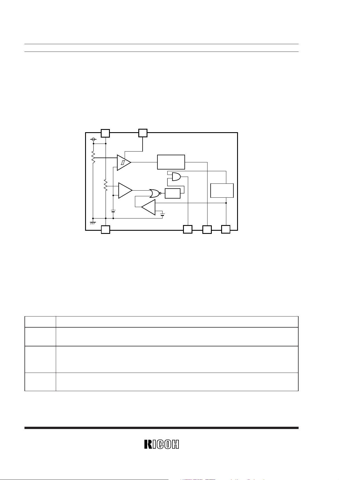
BLOCK DIAGRAM
• Over-charge/over-discharge protection for Li+ one-cell pack
• High precision protectors for cell-phones and any other gadgets using on board Li+ one-cell battery
SELECTION GUIDE
In the RN5VM1×××Series three of the input threshold for over-charge, over-discharge and excess current and taping type
can be designating at the user’s request by Part Number as follows:
RN5VM1
×××–×× ←Part Number
↑ ↑ ↑
a b c
VDD Ct
+
VD1
+
–
–
–
+
VD2
VD3
VSS
DOUT
COUT
V-
5
2
61
4
3
Level
Shift
Short Circuit
Detector
Delay
}
}
Code Description
a
Serial Number for the RN5VM Series designating input threshold for over-charge, over-discharge and
excess current detectors as well as hysteresis range for over-charge detector.
Designation of version symbols
b C : drawing load current is allowable after detecting over-charge.
D : drawing load current is not allowable after detecting over-charge.
c
Designation of Taping Type:
TR (refer to Taping Specification)
Page 7
3
RN5VM1××C/D
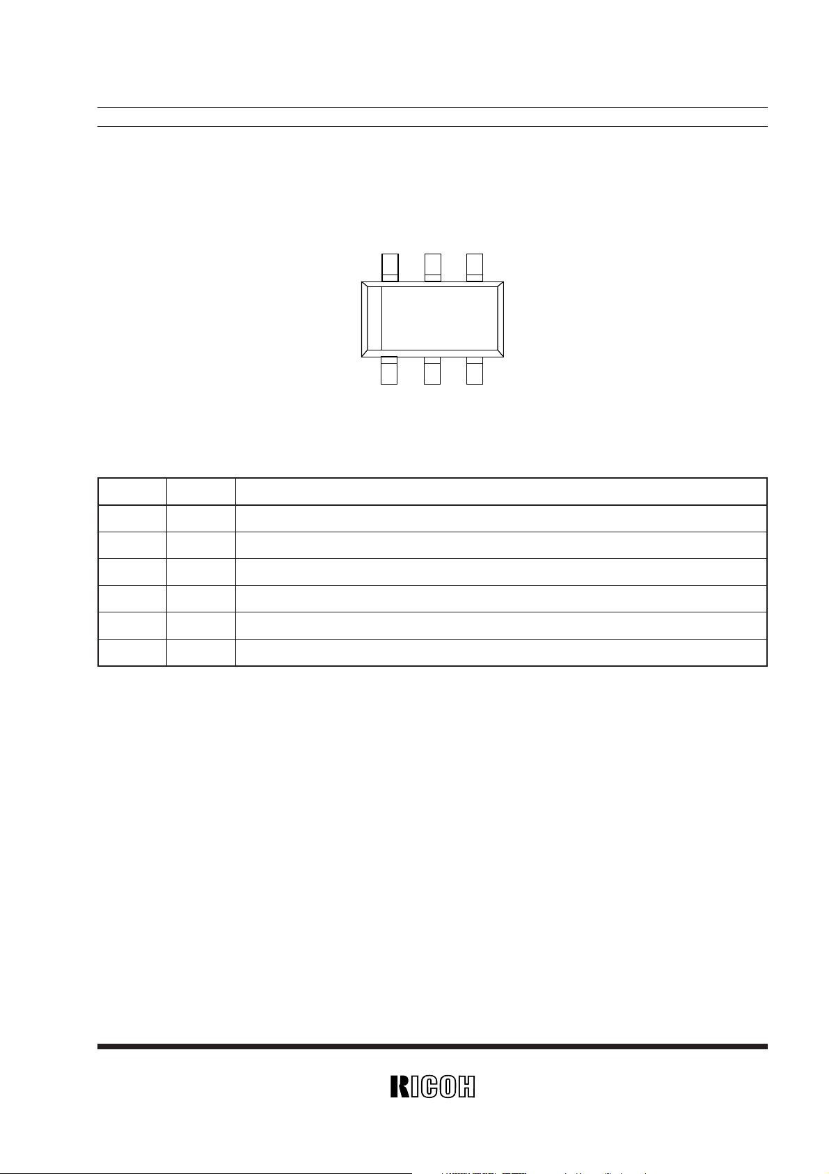
PIN CONFIGURATION
1 2
3
6 4
(mark side)
5
•SOT-23-6
PIN DESCRIPTION
Pin No. Symbol Pin description
1 COUT Output of over-charge detection, CMOS output
2 Ct Pin for external capacitor setting output delay of VD1
3 VSS Ground
4 DOUT Output of over-discharge detection, CMOS output
5 VDD Power supply
6 V- Pin for charger negative input
Page 8
RN5VM1××C/D
4
ABSOLUTE MAXIMUM RATINGS
Symbol Item Rating Unit
VDD Supply Voltage –0.3 to 12 V
V-
Input Voltage
V- pin V
DD–28 to VDD+0.3 V
Vct Ct pin Vss–0.3 to VDD+0.3 V
V
COUT
Output Voltage
C
OUT pin VDD–28 to VDD+0.3 V
VDOUT DOUT pin Vss–0.3 to VDD+0.3 V
PD Power Dissipation 150 mW
Topt Operating Temperature Range –40 to +85 ˚C
Tstg Storage Temperature Range –55 to +125 ˚C
ABSOLUTE MAXIMUM RATINGS
Absolute Maximum ratings are threshold limit values that must not be exceeded even for an instant under
any conditions. Moreover, such values for any two items must not be reached simultaneously. Operation
above these absolute maximum ratings may cause degradation or permanent damage to the device. These
are stress ratings only and do not necessarily imply functional operation below these limits.
Vss=0V
Page 9

5
RN5VM1××C/D
ELECTRICAL CHARACTERISTIC
Symbol Item Conditions MIN. TYP. MAX. Unit
VDD1 Operating input voltage Voltage defined as VDD–VSS 1.5 10 V
Vst
Minimum operating voltage Voltage defined as V
DD–V-,
1.2 V
for 0V charging V
DD–Vss=0V
VDET1 Over-charge threshold voltage Detect rising edge of supply voltage 4.20 4.25 4.30 V
VHYS1
Over-charge threshold hysteresis range
0.15 0.2 0.25 V
tVDET1 Output delay time of over-charge C3=0.01µF, VDD=3.6V→ 4.3V 50 75 100 ms
VDET2
Over-discharge threshold voltage Detect falling edge of supply voltage 2.437 2.50 2.563 V
tVDET2 Output delay time of over-discharge VDD=3.6V→ 2.4V 7 10 13 ms
VDET3 Excess current threshold voltage
Detect rising edge of “V-” pin voltage
0.17 0.20 0.23 V
tVDET3 Output delay time of excess current VDD=3.0V 9 13 17 ms
Vshort Short detection voltage VDD=3.0V VDD–1.1 VDD–0.8 VDD–0.5 V
tshort
Output delay time of short detection
VDD=3.0V 5 50 µs
Rshort
Reset resistance for
V
DD=3.6V, V-=1.0V 50 100 150 kΩ
excess current protection
VOL1 Nch ON voltage of COUT IOL=50µA, VDD=4.4V 0.2 0.5 V
VOH1 Pch ON voltage of COUT IOH=–50µA, VDD=3.9V 3.4 3.8 V
VOL2 Nch ON voltage of DOUT IOL=50µA, VDD=2.4V 0.2 0.5 V
VOH2 Pch ON voltage of DOUT IOH=–50µA, VDD=3.9V 3.4 3.7 V
IDD Supply current VDD=3.9V, V-=0V 3.0 6.0 µA
Istandby Standby current V
DD=2.0V 0.3 0.6 µA
Topt=25˚C
*
) Please refer to Test Circuit unless otherwise specified.
• RN5VM111C
Page 10

RN5VM1××C/D
6
Symbol Item Conditions MIN. TYP. MAX. Unit
VDD1 Operating input voltage Voltage defined as VDD–VSS 1.5 10 V
Vst
Minimum operating voltage Voltage defined as V
DD–V-,
1.2 V
for 0V charging VDD–Vss=0V
VDET1 Over-charge threshold voltage Detect rising edge of supply voltage 4.30 4.35 4.40 V
VHYS1
Over-charge threshold hysteresis range
0.15 0.20 0.25 V
tVDET1 Output delay time of over-charge C3=0.01µF, VDD=3.6V→ 4.4V 55 80 105 ms
VDET2 Over-discharge threshold voltage Detect falling edge of supply voltage 2.437 2.500 2.563 V
tVDET2 Output delay time of over-discharge VDD=3.6V→ 2.4V 7 10 13 ms
VDET3 Excess current threshold voltage
Detect rising edge of “V-” pin voltage
0.17 0.20 0.23 V
tVDET3 Output delay time of excess current VDD=3.0V 9 13 17 ms
Vshort Short detection voltage VDD=3.0V VDD–1.1 VDD–0.8 VDD–0.5 V
tshort
Output delay time of short detection
VDD=3.0V 5 50 µs
Rshort
Reset resistance for
V
DD=3.6V, V-=1.0V 50 100 150 kΩ
excess current protection
VOL1 Nch ON voltage of COUT IOL=50µA, VDD=4.4V 0.2 0.5 V
VOH1 Pch ON voltage of COUT IOH=–50µA, VDD=3.9V 3.4 3.8 V
VOL2 Nch ON voltage of DOUT IOL=50µA, VDD=2.4V 0.2 0.5 V
VOH2 Pch ON voltage of DOUT IOH=–50µA, VDD=3.9V 3.4 3.7 V
IDD Supply current VDD=3.9V, V-=0V 3.0 6.0 µA
Istandby Standby current V
DD=2.0V 0.3 0.6 µA
Topt=25˚C
*
) Please refer to Test Circuit unless otherwise specified.
• RN5VM112C
Page 11

7
RN5VM1××C/D
Symbol Item Conditions MIN. TYP. MAX. Unit
VDD1 Operating input voltage Voltage defined as VDD–VSS 1.5 10 V
Vst
Minimum operating voltage Voltage defined as V
DD–V-,
1.2 V
for 0V charging VDD–Vss=0V
VDET1 Over-charge threshold voltage Detect rising edge of supply voltage 4.20 4.25 4.30 V
VHYS1
Over-charge threshold hysteresis range
0.15 0.20 0.25 V
tVDET1 Output delay time of over-charge C3=0.01µF, VDD=3.6V→ 4.3V 50 75 100 ms
VDET2 Over-discharge threshold voltage Detect falling edge of supply voltage 2.437 2.500 2.563 V
tVDET2 Output delay time of over-discharge VDD=3.6V→ 2.4V 7 10 13 ms
VDET3 Excess current threshold voltage
Detect rising edge of “V-” pin voltage
0.17 0.20 0.23 V
tVDET3 Output delay time of excess current VDD=3.0V 9 13 17 ms
Vshort Short detection voltage VDD=3.0V VDD–1.1 VDD–0.8 VDD–0.5 V
tshort
Output delay time of short detection
VDD=3.0V 5 50 µs
Rshort
Reset resistance for
V
DD=3.6V, V-=1.0V 50 100 150 kΩ
excess current protection
VOL1 Nch ON voltage of COUT IOL=50µA, VDD=4.4V 0.2 0.5 V
VOH1 Pch ON voltage of COUT IOH=–50µA, VDD=3.9V 3.4 3.8 V
VOL2 Nch ON voltage of DOUT IOL=50µA, VDD=2.4V 0.2 0.5 V
VOH2 Pch ON voltage of DOUT IOH=–50µA, VDD=3.9V 3.4 3.7 V
IDD Supply current VDD=3.9V, V-=0V 3.0 6.0 µA
Istandby Standby current V
DD=2.0V 0.3 0.6 µA
Topt=25˚C
*
) Please refer to Test Circuit unless otherwise specified.
• RN5VM111D
Page 12

RN5VM1××C/D
8
Symbol Item Conditions MIN. TYP. MAX. Unit
VDD1 Operating input voltage Voltage defined as VDD–VSS 1.5 10 V
Vst
Minimum operating voltage Voltage defined as V
DD–V-,
1.2 V
for 0V charging VDD–Vss=0V
VDET1 Over-charge threshold voltage Detect rising edge of supply voltage 4.30 4.35 4.40 V
VHYS1
Over-charge threshold hysteresis range
0.15 0.20 0.25 V
tVDET1 Output delay time of over-charge C3=0.01µF, VDD=3.6V→ 4.4V 55 80 105 ms
VDET2 Over-discharge threshold voltage Detect falling edge of supply voltage 2.437 2.500 2.563 V
tVDET2 Output delay time of over-discharge VDD=3.6V→ 2.4V 7 10 13 ms
VDET3 Excess current threshold voltage
Detect rising edge of “V-” pin voltage
0.17 0.20 0.23 V
tVDET3 Output delay time of excess current VDD=3.0V 9 13 17 ms
Vshort Short detection voltage VDD=3.0V VDD–1.1 VDD–0.8 VDD–0.5 V
tshort
Output delay time of short detection
VDD=3.0V 5 50 µs
Rshort
Reset resistance for
V
DD=3.6V, V-=1.0V 50 100 150 kΩ
excess current protection
VOL1 Nch ON voltage of COUT IOL=50µA, VDD=4.4V 0.2 0.5 V
VOH1 Pch ON voltage of COUT IOH=–50µA, VDD=3.9V 3.4 3.8 V
VOL2 Nch ON voltage of DOUT IOL=50µA, VDD=2.4V 0.2 0.5 V
VOH2 Pch ON voltage of DOUT IOH=–50µA, VDD=3.9V 3.4 3.7 V
IDD Supply current VDD=3.9V, V-=0V 3.0 6.0 µA
Istandby Standby current V
DD=2.0V 0.3 0.6 µA
Topt=25˚C
*
) Please refer to Test Circuit unless otherwise specified.
• RN5VM112D
Page 13

9
RN5VM1××C/D
TIMING DIAGRAM
• RN5VM1××C
Charging Charging
Charging
Charging
Discharging
Discharging
Discharging
Excess
current
Short
circuit
Open Open
Charging
Current
Discharging
Current
0
DOUT
COUT
VDD
V-
t
t
t
t
t
VSS
VSS
VDD
VDD
VDD
VDET2
VDET1
VDET3
VDET1–VHYS1
Vshort
V-
tVDET1
tVDET1
tVDET2 tVDET2 tVDET3 tshort
Charging/
Discharging
Current
Page 14

RN5VM1××C/D
10
• RN5VM1××D
Charging
Charging
Charging
Discharging
Discharging
Discharging
Open
Open
Open
0
DOUT
COUT
VDD
V-
t
t
t
t
t
V
SS
VSS
VDD
VDD
VDD
VDET2
VDET1
VDET3
VDET1–VHYS1
Vshort
V-
Self
discharging
tVDET1
tVDET3
tVDET2 tVDET2
tVDET3 tshort
Charging
Current
Discharging
Current
Excess
current
Short
circuit
Charging/
Discharging
Current
Page 15

11
RN5VM1××C/D
OPERATION
· The VD1 monitors VDD pin voltage. When the VDD voltage crosses over-charge detector threshold VDET1 from a low val-
ue to a value higher than the V
DET1, the VD1 can sense over-charging and an external charge control Nch-MOS-FET
turns to “OFF” with C
OUT pin being at “L”.
· An output delay time for over-charge detection can be set by an external capacitor C
3 connecting the Vss pin and Ct pin.
The external capacitor can make a delay time from a moment detecting over-charge to a time output a signal which
enables charge control Nch-MOS-FET for turning to “OFF”. Though the V
DD voltage would be going up to a higher lev-
el than V
DET1 if it is within a time period of the output delay time, VD1 would not output a signal for turning “OFF” of
charg control Nch-MOS-FET. The output delay time can be calculated as below:
tVDET1 =
C
3 ×
(
VDD– 0.7
)
0.48 × 10
–6
· A level shifter incorporated in a buffer driver for the COUT pin makes the “L” of COUT pin to the V- pin voltage and the “H”
of C
OUT pin is set to VDD voltage with CMOS buffer.
• VD1/Over-Charge Detector
· After detecting over-charge, the VD1 would not be released and C
OUT level would not switch to “H” again with the excep-
tion that a cell voltage reaches to a lower value than “V
DET1–VHYS1” by self discharge of cell or else. After detecting over-
charge, when the V
DD level stays at a value higher than “VDET1–VHYS1”, to connect battery pack to a system load makes
battery pack being disabled at for charging or discharging because of excess current detector operated being D
OUT “L”.
Reset conditions from overcharging of RN5VM1
××C
· There can be two cases to reset the VD1 making the COUT pin level to “H” again after detecting over-charge. Resetting
the VD1 makes the charging system ready for resumption of charging process.
The first case is in such condition that a time when the V
DD voltage is coming down to a level lower than “VDET1–VHYS1”.
While in the second case, disconnecting a charger from the battery pack can make the VD1 resetting when the V
DD lev-
el is within hysteresis width (V
DET1–VHYS1≤VDD
<
V
DET1)
· After detecting over-charge with the V
DD voltage of higher than VDET1, connecting system load to the battery pack makes
load current allowable through parasitic diode of external charge control Nch-MOS-FET. The C
OUT level would be “H”
when the V
DD level is coming down to a level below the VDET1 by continuous drawing of load current.
Reset conditions from overcharging of RN5VM1
××D
Page 16

RN5VM1××C/D
12
· The VD2 monitors a VDD pin voltage. When the VDD voltage crosses the over-discharge detector threshold VDET2 from
a high value to a value lower than the V
DET2, the VD2 can sense an over-discharging and the external discharge control
Nch-MOS-FET turns to “OFF” with the D
OUT pin being at “L”.
· Resetting the VD2 with the D
OUT pin level being “H” again after detecting over-discharge is only possible by connecting
a charger to the battery pack. When the V
DD voltage stays under over-discharge detector threshold VDET2 charge current
can flow through parasitic diode of external discharge control Nch-MOS-FET, then after the V
DD voltage comes up to a
value larger than V
DET2 discharging process would be advanced through “ON” state discharge control Nch-MOS-FET.
Connecting a charger to the battery pack makes the D
OUT level being “H” instantaneously when the VDD voltage is high-
er than V
DET2.
· When a cell voltage equals to zero, connecting charger to the battery pack makes the system allowable for charge with
higher charge voltage than Vst, 1.2V Max.
· An output delay time for the over-discharge detection is fixed internally. Though the V
DD voltage would be going down
to a lower level than V
DET2 if it is within a time period of the output delay time, VD2 would not output a signal for turning
“OFF” of discharge control Nch-MOS-FET.
· After detection of an over-discharge by VD2, supply current would be reduced to 0.3µA TYP. at V
DD=2.0V and into stand-
by, only the charger detector is operating.
· The output type of D
OUT pin is CMOS having “H” level of VDD and “L” level of Vss.
• VD2/Over-Discharge Detector
· Both of the excess current detector and short circuit protector can work when both control Nch-MOS-FETs are in “ON”
state.
When the V- pin voltage is going up to a value between the short protection voltage Vshort and excess current threshold
V
DET3, the excess current detector operates and further soaring of V- pin voltage higher than Vshort makes the short cir-
cuit protector enabled. As a result the external discharge control Nch-MOS-FET turns to “OFF” with the D
OUT pin being
at “L”.
· An output delay time for the excess current detector is internally fixed, 13ms TYP. at V
DD=3.0V. A quick recovery of V-
pin level from a value between Vshort and V
DET3 within the delay time keeps the discharge control FET staying
“ON”state.
When the short circuit protector is enabled, the D
OUT would be “L” and its delay time would be 5µs TYP.
· The V- pin has a built-in pull down resistor, TYP.100kΩ, connected to the Vss pin.
After an excess current or short circuit protection is detected, removing a cause of excess current or external short cir-
cuit makes an external discharge control Nch-MOS-FET to an “ON” state automatically with the V- pin level being down
to the Vss level through the built-in pull down resistor.
· When V
DD voltage is higher than VDET2 at a time when the excess current is detected the 5VM does not enter a standby
mode, while V
DD voltage is lower than VDET2 the 5VM enters a standby mode.
After detecting short circuit the 5VM will not enter a standby mode.
• VD3/Excess Current Detector, Short Circuit Protector
Page 17

13
RN5VM1××C/D
TEST CIRCUIT
VDD
VSS
V-
C
OUT
Ct
V
0.01µF
1
3
5
6
2
Test Circuit 1
VDD
VSS
V-
D
OUT
V
4
3
5
6
Test Circuit 2
DOUT
VDD
VSS
V-
1
5
V
3
6
50µA
Test Circuit 5
DOUT
VDD
VSS
V-
4
5
V
3
6
50µA
Test Circuit 6
DOUT
VDD
VSS
V-
3
5
6
V
A
4
Test Circuit 3
COUT
VDD
VSS
V-
5
V
3
6
50µA
1
Test Circuit 4
Page 18

RN5VM1××C/D
14
DOUT
VDD
VSS
V-
5
V
3
6
50µA
4
Test Circuit 7
VDD
VSS
V-
3
5
6
A
Test Circuit 8
COUT
C3
C1
R1
Ct
V
DD
VSS
V-
V
3
6
5
2
1
Test Circuit 9
DOUT
VDD
VSS
V-
R
2
C2
3
4
5
6
V
Test Circuit 10
The typical characteristics were obtained by use of these test circuits
Test Circuit 1 : Typical characteristics 1) 5) 9) 16)
Test Circuit 2 : Typical characteristics 2) 6)
Test Circuit 3 : Typical characteristics 3) 4) 7) 8) 18)
Test Circuit 4 : Typical characteristics 12)
Test Circuit 5 : Typical characteristics 13)
Test Circuit 6 : Typical characteristics 14)
Test Circuit 7 : Typical characteristics 15)
Test Circuit 8 : Typical characteristics 10) 11)
Test Circuit 9 : Typical characteristics 20)
Test Circuit 10 : Typical characteristics 17) 19)
Page 19

15
RN5VM1××C/D
TYPICAL CHARACTERISTICS
1) Over-charge threshold vs. Temperature
Over-charge Threshold VDET1(V)
Temperature Topt (˚C)
4.20
4.21
4.22
4.23
4.24
4.25
4.26
4.27
–60 –40 –20 0 20 40 60 80 100
RN5VM111×
3) Excess Current Threshold vs. Temperature
Temperature Topt (˚C)
Excess Current Threshold VDET3(V)
0.190
0.195
0.200
0.205
0.210
–60 –40 –20 0 20 40 60 80 100
RN5VM111×/112×
5) Output Delay of Over-charge vs. Temperature
20
30
40
50
60
70
80
90
100
–60 –40 –20 0 20 40 60 80 100
Output Delay of Over-charge
tVDET1(ms)
RN5VM111×
Temperature Topt (˚C)
C3=0.01µF, VDD=3.6V→4.3V
2) Over-discharge vs. Temperature
Temperature Topt (˚C)
Over-discharge Threshold VDET2(V)
2.47
2.48
2.49
2.50
2.51
2.52
2.53
2.54
–60 –40 –20 0 20 40 60 80 100
RN5VM111×/112×
4) Short circuit protector Threshold vs. Temperature
2.10
2.15
2.20
2.25
2.30
2.35
2.40
–60 –40 –20 0 20 40 60 80 100
RN5VM1×××
Temperature Topt (˚C)
V
DD=3.0V
Short circuit protector Threshold Vshort(V)
6) Output Delay of Over-discharge vs. Temperature
2
4
6
8
10
12
14
16
18
–60 –40 –20 0 20 40 60 80 100
Temperature Topt (˚C)
Output Delay of Over-discharge
tVDET2(ms)
RN5VM111×/112×
VDD=3.6V→2.4V
Page 20

RN5VM1××C/D
16
7) Output Delay of Excess current vs. Temperature
Temperature Topt (˚C)
0
2
4
6
8
10
12
14
16
18
20
–60 –40 –20 0 20 40 60 80 100
RN5VM1×××
Output Delay of Excess current
tVDET3(ms)
VDD=3.0V
9)
Over-charge Threshold Hysteresis vs.Temperature
Over -charge Treshold Hysteresis V
HYS1
(mV)
Temperature Topt (˚C)
0.190
0.195
0.200
0.205
0.210
–60 –40 –20 0 20 40 60 80 100
RN5VM111×/112×
11) Standby Current vs. Temperature
Standby Current Istandby(µA)
Temperature Topt (˚C)
0.00
0.05
0.10
0.15
0.20
0.25
0.30
0.35
0.40
–60 –40 –20 0 20 40 60 80 100
RN5VM1×××
VDD=2.0V
8)
Output Delay of Short circuit protector vs. Temperature
Output Delay of Short circuit
protector
tshort(µs)
Temperature Topt (˚C)
0
2
4
6
8
10
–60 –40 –20 0 20 40 60 80 100
RN5VM1×××
VDD=3.0V
10) Supply Current vs. Temperature
Supply Current IDD(µA)
Temperature Topt (˚C)
0.0
0.5
1.0
1.5
2.0
2.5
3.0
3.5
4.0
–60 –40 –20 0 20 40 60 80 100
RN5VM1×××
VDD=3.9V, V-=0V
Page 21

17
RN5VM1××C/D
12) Cout Nch Driver On Voltage vs. Temperature
C
OUT
Nch Driver ON Voltage V
OL1
(V)
IOL=50µA,VDD=4.4V
Temperature Topt (˚C)
0.00
0.05
0.10
0.15
0.20
0.25
0.30
–60 –40 –20 0 20 40 60 80 100
RN5VM1×××
14) DOUT Nch Driver ON Voltage vs. Temperature
D
OUT
Nch Driver ON Voltage V
OL2
(V)
IOL=50µA,VDD=2.4V
Temperature Topt (˚C)
0.00
0.05
0.10
0.15
0.20
0.25
0.30
–60 –40 –20 0 20 40 60 80 100
RN5VM1×××
13) COUT Pch Driver ON Voltage vs. Temperature
C
OUT
Pch Driver ON Voltage V
OH1
(V)
IOH=–50µA,VDD=3.9V
Temperature Topt (˚C)
3.60
3.65
3.70
3.75
3.80
3.85
3.90
–60 –40 –20 0 20 40 60 80 100
RN5VM1×××
15) DOUT Pch Driver ON Voltage vs. Temperature
D
OUT
Pch Driver ON Voltage V
OH2
(V)
IOH=–50µA,VDD=3.9V
Temperature Topt (˚C)
3.60
3.65
3.70
3.75
3.80
3.85
3.90
–60 –40 –20 0 20 40 60 80 100
RN5VM1×××
Page 22

RN5VM1××C/D
18
16)
Output Delay of Over-charge vs. Capacitance C
3
External Capacitance C3(µF)
Output Delay of Over-charge
t
VDET1
(ms)
200
100
0
300
400
500
600
700
800
0 0.05 0.1
RN5VM111×
VDD=3.6V→4.3V
18) Output Delay of Excess Current vs. VDD
Output Delay of Excess Current tVDET3(ms)
Supply Voltage VDD(V)
0.00
5.00
10.00
15.00
20.00
25.00
2.5 3.0 3.5 4.0 4.5
RN5VM1×××
20)
Over-charge Threshold vs. External Resistance R
1
Over-charge Threshold VDET1(V)
External Resistance R1(Ω)
C1=0 to 0.68µF
0 200 400 600 800 1000
RN5VM111×
4.250
4.246
4.252
4.254
4.256
4.258
C3=0.22µF
4.248
C3=0.1µF
C3=0.01µF
17)
Output Delay of Short protection vs. Capacitance C
2
External Capacitance C2(µF)
Output Delay of short protection
t
short(µs)
1
10
100
1000
10000
0.001 0.01 0.1 1
RN5VM1×××
R2=1kΩ,VDD=3.0V
19)
Excess Current Threshold vs. External resistance R
2
Excess Current Threshold
t
DET3
(ms)
VDD=3.0V
0.202
0.203
0.204
0.205
0.206
0.207
0.208
0.209
0.210
0 0.5 1 1.5 2 2.5 3
RN5VM111×/112×
External Resistance R2(kΩ)
Page 23

19
RN5VM1××C/D
TYPICAL APPLICATION
3
4 1
2
5
6
+
–
RN5VM1×××
1kΩ
R
2
C2
100Ω
R
1
0.1µF
VDD
V-
DOUT COUT
Vss
Ct
C1
C3
0.1µF
0.01µF
NOTE ON EXTERNAL COMPONENTS
•R1 and C1 will stabilize a supply voltage to the RN5VM. A recommended R1 value is less than 1kΩ.
A larger value of R
1 leads higher detection voltage, makes some errors, because of shoot through current
flowed in the RN5VM.
•R
2 and C2 will stabilize a V- pin voltage. The resetting from over-discharge with connecting charger possibly
be disabled by larger value of R
2. Recommended value is less than 1kΩ.
After an over-charge detection, a system may not draw load current when a battery pack is connected to it in
the C version with R2 and C2 time constants at relatively larger settings.
Recommended C
2 value is less than 1µF.
•R
1 and R2 can operate as a current limiter against setting cell reverse direction or for applying excess
charging voltage to the 5VM. While smaller R
1 and R2 may cause an over power dissipation rating of the
RN5VM and a total of “R
1+R2” should be more than 1kΩ.
•The time constants R
1×C1 or R2×C2 must have a relations as below:
R
1×C1≤R2 ×C2
Because in case that R1×C1, time constant for VDD pin, would be larger than R2×C2, time constant for V- pin,
then the RN5VM might be into a standby mode after detecting excess current or short circuit current.
Page 24

RN5VM1××C/D
20
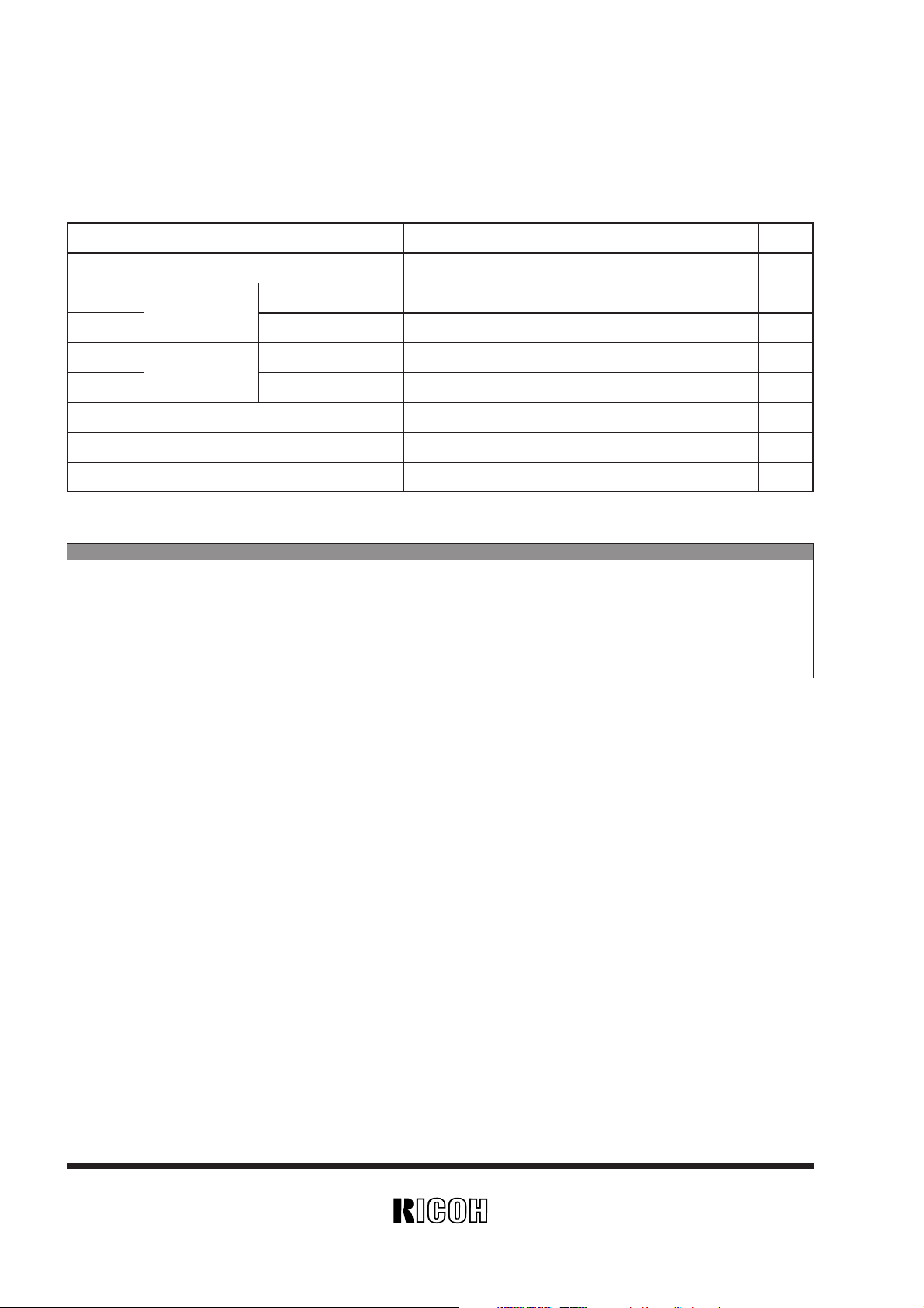
PACKAGE DIMENSION (Unit : mm)
· SOT-23-6
TAPING SPECIFICATION (Unit : mm)
· SOT-23-6
2.9±0.2
0.8±0.1
+0.1
–0.2
0.4
1.9±0.2
(0.95) (0.95)
6 5 4
1 2 3
+0.2
–0.1
1.6
+0.2
–0.1
1.1
+0.1
–0.05
0.15
2.8±0.3
0 to 0.1
0.2 MIN.
User Direction of Feed
T R
2.0MAX.
0.3±0.1
4.0±0.1
2.0±0.05
4.0±0.1
3.3
3.2
8.0±0.3
1.75±0.1
3.5±0.05
1.5
+0.1
–0
ø
Page 25

RICOH COMPANY, LTD.
ELECTRONIC DEVICES DIVISION
HEADQUARTERS
13-1, Himemuro-cho, Ikeda City, Osaka 563-8501, JAPAN
Phone 81-727-53-1111 Fax 81-727-53-6011
YOKOHAMA OFFICE (International Sales)
3-2-3, Shin-Yokohama, Kohoku-ku, Yokohama City, Kanagawa 222-8530,
JAPAN
Phone 81-45-477-1697 Fax 81-45-477-1694 • 1695
http://www.ricoh.co.jp/LSI/english/
RICOH CORPORATION
ELECTRONIC DEVICES DIVISION
SAN JOSE OFFICE
3001 Orchard Parkway, San Jose, CA 95134-2088, U.S.A.
Phone 1-408-432-8800 Fax 1-408-432-8375
 Loading...