

Page 1
Raytheon RF Components
362 Lowell Street
Andover, MA 01810
www.raytheonrf.com
ADVANCED INFORMATION
Revised November 14, 2001
Page 1
Characteristic performance data and specifications are subject to change without notice.
Description
Single positive-supply operation and power-down mode
Low backed-off power current consumption: 75 mA @ 12 dBm Pout
30% power-added efficiency at +28.5 dBm CDMA average output power
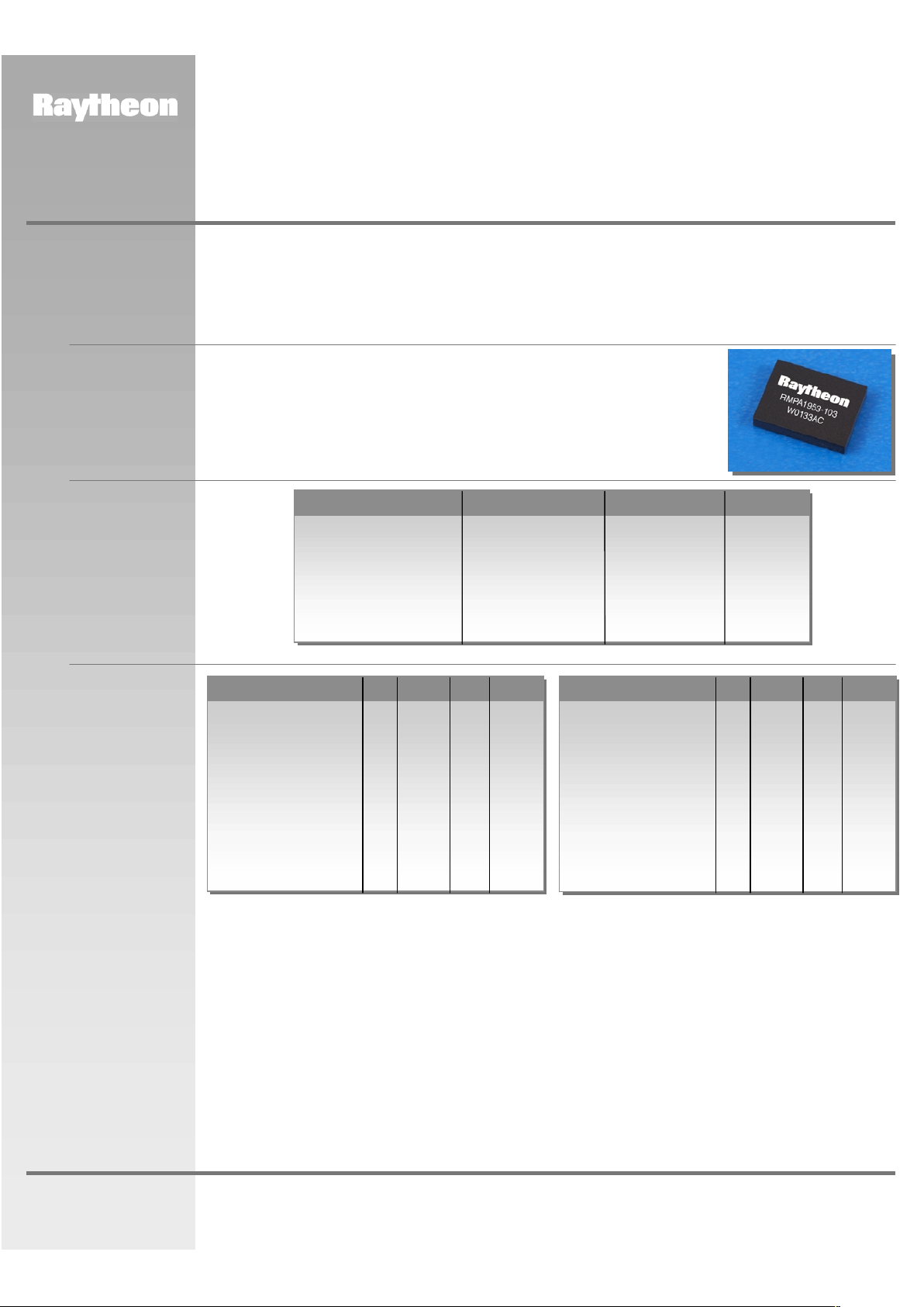
Compact LCC package: 6.0 x 8.0 x 1.5 mm
3
50 ohm matched and DC blocked input/output
Advanced Digital Bias Control and DC Power Management
Features
The RMPA1953-103 is a power amplifier for CDMA and CDMA2000-1X personal communications system (PCS)
applications. The PA is internally matched to 50 ohms to minimize the use of external components. Advanced DC
power management reduces current consumption during peak phone usage at backed-off RF power levels.
Advanced digital bias control reduces the number of interface components to baseband. High power-added
efficiency and excellent linearity are achieved using Raytheon’s InGaP Heterojunction Bipolar Transistor (HBT)
technology.
RMPA1953-103
3V PCS CDMA & CDMA2000 Power Amplifier
Module with Digital Bias Control
Electrical
Characteristics
2
Parameter Min Typ Max Unit
Operating Frequency 1850 1910 MHz
Gain
(Po=12 dBm) 22 28 dB
(Po=28.5 dBm) 27 30 34 dB
Linear Output Power 28.5 dBm
CDMA PAE
(Po=28.5 dBm) 30 %
(Po=19 dBm) 8 %
ACPR
3
-47 -51 dBc
ACPR2
4
-56 dBc
Parameter Min Typ Max Unit
Noise Power
(Po ≤ 28.5 dBm) -137 dBm/Hz
Input VSWR (50Ω) 2.0:12.5:1
Itotal @28.5 dBm Pout 680 mA
Itotal @12 dBm Pout 75 mA
Stability (All spurious)
5
-65 dBc
Harmonics (Po ≤ 28.5 dBm)
2fo, 3fo, 4fo -30 dBc
Power Shutdown Current
6
<1 uA
Vcc 3.1 3.4 4.6 V
Notes:
1. No permanent damage with only one parameter set at extreme limit. Other parameters set to typical values.
2. All parameters met at Tc =+25°C, Vcc =+3.4V, Vref=+2.9V, f=1880 MHz and load VSWR ≤ 1.2:1.
3. Po ≤ 28.5 dBm at Vcc=3.4V; CDMA Waveform measured using the ratio of average power within a 1.23 MHz channel to average power
within a 30 kHz bandwidth at + 1.25 MHz offset.
4. Po ≤ 28.5 dBm at Vcc=3.4V; CDMA Waveform measured using the ratio of average power within a 1.23 MHz channel to average power
within a 30 kHz bandwidth at +1.98 MHz offset.
5. Output VSWR ≤ 6:1, all phase angles.
6. No applied RF signal. Vcc=+3.4V nominal, Venbl=+0.2V maximum.
Absolute
Maximum
Ratings
1
Parameter Symbol Value Unit
Supply Voltages Vcc1, Vcc2, and Vbias 5 V
Bias Voltage 1 and 2 Vba1, Vba2 2.5 V
Chip Enable Venbl 3.0 V
RF Input Power Pin +5 dBm
Case Operating Temperature Tc -30 to +85 °C
Storage Temperature Tstg -55 to +150 °C
Page 2
Raytheon RF Components
362 Lowell Street
Andover, MA 01810
www.raytheonrf.com
ADVANCED INFORMATION
Revised November 14, 2001
Page 2
Characteristic performance data and specifications are subject to change without notice.
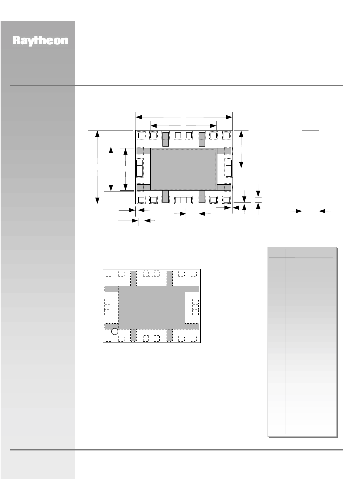
1.5
SIDE
TOP VIEW
(Through Package)
GND
171819 16 131415 12
32147658
10
21
9
11
20
22
RF OUT
RF IN
Venbl
Vref
Vld
Vcc1
Vbias
Vcc2
NC
NC
NC
Vba1
Vba2
Gnd
Gnd
Gnd
Gnd
6.0
1.00
0.50
BOTTOM VIEW
0.10
0.25
3.0
3.5 3.3
8.0
5.5
0.10
0.50
1
2
3
4
5
6
7
8
9
10
11
12
13
14
15
16
17
18
19
20
21
22
Vref
Venbl
GND
Vba1 and Vba2
Vba1 and Vba2
GND
NC
NC
GND
RF Out
GND
Vld
NC
GND
Vcc2
Vcc2
GND
Vcc1
Vbias
GND
RF In
GND
DescriptionPin #
Figure 1
Package Outline and Pin
Designations
Dimensions in mm
0.5mm x 0.5mm pad at 1.0mm pitch
RMPA1953-103
3V PCS CDMA & CDMA2000 Power Amplifier
Module with Digital Bias Control
Page 3
Raytheon RF Components
362 Lowell Street
Andover, MA 01810
www.raytheonrf.com
ADVANCED INFORMATION
Revised November 14, 2001
Page 3
Characteristic performance data and specifications are subject to change without notice.
RMPA1953-103
3V PCS CDMA & CDMA2000 Power Amplifier
Module with Digital Bias Control
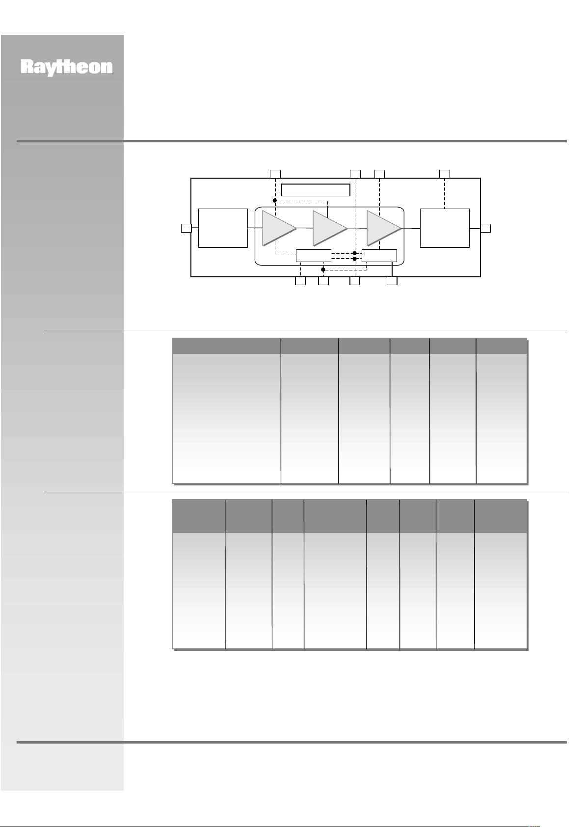
Figure 2
Functional Block
Diagram
Parameter Symbol Value Unit Max Units
Supply Voltage Vcc 3.1 3.4 4.5 V
RF Input Power
1
Pin -89 0 +3 dBm
CDMA Output Power Range Pout -55 +28.5 dBm
Vld Hi Power Vld floating V
Vld Low Power Vld 2.5 2.9 V
Bias Control hi Vba1 and 2 2.38 2.83 V
Bias Control low Vba1 and 2 0.00 0.45 V
Enable Control Voltage high Ven_hi 2.38 2.83 V
Enable Contol Voltage low Ven_lo 0.00 0.45 V
Reference Voltage Vref 2.9 3.50 V
Recommended
Operating Conditions
Operational Control
Typical RF input power for
CDMA Pout = +28.5 dBm
Vcc1, 2 and
Vba1 and Vld Vbias Pins Venbl Pout PAE Itotal
Vba2 Pins Pin (V) Tied Together Pin (V) (dBm) (%) typ. (mA) typ.
High Power 2.5V Lo 3.4 V 2.7 28.5 30 680
Operation CDMA High
Power
Threshold 0V Hi 3.4 V 2.7 19.0 15 150
Power 2.7 CDMA
Operation Threshold
power for Vld
High Switch
Low Power 0V Hi 3.4 V
Operation 2.7 CDMA Low 2.7 12.0 6 75
Power
RF OUT
Output
Match
Interstage Match
Bias
Vba1 Venbl Vba2
Bias
Input
Match
Vref
Vcc2 VldVcc1 Vbias
RF IN
Page 4

Raytheon RF Components
362 Lowell Street
Andover, MA 01810
www.raytheonrf.com
ADVANCED INFORMATION
Revised November 14, 2001
Page 4
Characteristic performance data and specifications are subject to change without notice.
RMPA1953-103
3V PCS CDMA & CDMA2000 Power Amplifier
Module with Digital Bias Control
Figure 3
Common Control of
Cellular and PCS
band PAs
Vba2
RF IN
Vcc1
Vcc2
Vbias
NC
Vref
NC
NC
Vld
21 4
7 8
1819
16 15
13 12
21
Venbl
Vba1
RMPA1953
Vba2
RF IN
Vcc1
Vcc2
Vbias
NC
Vref
Vld
21
Venbl
Vba1
RMPA0953
Vref
CELL Band Enable
Vba1 & 2
PCS Band Enable
Vcc
RF OUT
10
RF OUT
10
5
1819 16 15 13 12
NC
NC
21 4 7 85
Page 5

Raytheon RF Components
362 Lowell Street
Andover, MA 01810
www.raytheonrf.com
ADVANCED INFORMATION
Revised November 14, 2001
Page 5
Characteristic performance data and specifications are subject to change without notice.
RMPA1953-103
3V PCS CDMA & CDMA2000 Power Amplifier
Module with Digital Bias Control
Application
Information
Precautions to Avoid Permanent Device Damage:
– Cleanliness: Observe proper handling procedures to ensure clean devices and PCBs. Devices should remain
in their original packaging until component placement to ensure no contamination or damage to RF, DC &
ground contact areas.
− Device Cleaning: Standard board cleaning techniques should not present device problems provided that the
boards are properly dried to remove solvents or water residues.
− Static Sensitivity: Follow ESD precautions to protect against ESD damage:
A properly grounded static-dissipative surface on which to place devices.
Static-dissipative floor or mat.
A properly grounded conductive wrist strap for each person to wear while handling devices.
− General Handling: Handle the package on the top with a vacuum collet or along the edges with a sharp pair
of bent tweezers. Avoiding damaging the RF, DC, & ground contacts on the package bottom. Do not apply
excessive pressure to the top of the lid.
− Device Storage: Devices are supplied in heat-sealed, moisture-barrier bags. In this condition, devices are
protected and require no special storage conditions. Once the sealed bag has been opened, devices should
be stored in a dry nitrogen environment.
Device Usage: Raytheon recommends the following procedures prior to assembly.
− Dry-bake devices at 125°C for 24 hours minimum. Note: The shipping trays cannot withstand 125°C baking
temperature.
− Assemble the dry-baked devices within 7 days of removal from the oven.
− During the 7-day period, the devices must be stored in an environment of less than 60% relative humidity
and a maximum temperature of 30
°C
− If the 7-day period or the environmental conditions have been exceeded, then the dry-bake procedure must
be repeated.
Solder Materials & Temperature Profile: Reflow soldering is the preferred method of SMT attachment. Hand
soldering is not recommended.
− Reflow Profile
Ramp-up: During this stage the solvents are evaporated from the solder paste. Care should be taken to
prevent rapid oxidation (or paste slump) and solder bursts caused by violent solvent out-gassing. A
typical heating rate is 1- 2°C/sec.
Pre-heat/soak: The soak temperature stage serves two purposes; the flux is activated and the board
and devices achieve a uniform temperature. The recommended soak condition is: 120-150 seconds at
150°C.
Reflow Zone: If the temperature is too high, then devices may be damaged by mechanical stress due to
thermal mismatch or there may be problems due to excessive solder oxidation. Excessive time at
temperature can enhance the formation of inter-metallic compounds at the lead/board interface and
may lead to early mechanical failure of the joint. Reflow must occur prior to the flux being completely
driven off. The duration of peak reflow temperature should not exceed 10 seconds. Maximum soldering
temperatures should be in the range 215-220°C, with a maximum limit of 225°C.
Cooling Zone: Steep thermal gradients may give rise to excessive thermal shock. However, rapid
cooling promotes a finer grain structure and a more crack-resistant solder joint. Figure 1 indicates the
recommended soldering profile.
Solder Joint Characteristics: Proper operation of this device depends on a reliable void-free attachment of the
heatsink to the PWB. The solder joint should be 95% void-free and be a consistent thickness.
Rework Considerations: Rework of a device attached to a board is limited to reflow of the solder with a heat
gun. The device should not be subjected to more than 225°C and reflow solder in the molten state for more than
5 seconds. No more than 2 rework operations should be performed.
Page 6

Raytheon RF Components
362 Lowell Street
Andover, MA 01810
www.raytheonrf.com
ADVANCED INFORMATION
Revised November 14, 2001
Page 6
Characteristic performance data and specifications are subject to change without notice.
RMPA1953-103
3V PCS CDMA & CDMA2000 Power Amplifier
Module with Digital Bias Control
Figure 4
Recommended Solder
Reflow Profile
183°C
10 Sec
0
20
40
60
80
100
120
140
160
180
200
220
240
0 60 120 180 240 300
Time (Sec)
Deg C
1°C/Sec
Soak at
150°C for
60 Sec
45 Sec
(Max)
above
183°C
1°C/Sec
Page 7

Raytheon RF Components
362 Lowell Street
Andover, MA 01810
www.raytheonrf.com
ADVANCED INFORMATION
Revised November 14, 2001
Page 7
Characteristic performance data and specifications are subject to change without notice.
Vld HiVld Lo
28.5 24 19 12
CDMA ACPR1 and ACPR2 vs. Power Output
Vcc=3.4, T=20°C
Current and CDMA PAE vs. Output Power
Vcc=3.4, T=20°C
ACPR (dBc)
Output Power (dBm)
70
65
60
55
50
45
40
RMPA1953-103
3V PCS CDMA & CDMA2000 Power Amplifier
Module with Digital Bias Control
Performance
Data
Itotal (mA)
Output Power (dBm)
0
100
400
500
600
700
800
0
5
10
15
20
25
30
35
PAE (%)
200
300
PAE
Vld HiVld Lo
28.5241912
Itotal
PAE
Itotal
ACPR1
ACPR2
Page 8

Raytheon RF Components
362 Lowell Street
Andover, MA 01810
www.raytheonrf.com
ADVANCED INFORMATION
Revised November 14, 2001
Page 8
Characteristic performance data and specifications are subject to change without notice.
D&L Technical Sales
6139 S. Rural Road, #102
Tempe, AZ 85283
480-730-9553
fax: 480-730-9647
Nicholas Delvecchio, Jr.
dlarizona@aol.com
Hi-Peak Technical Sales
P.O. Box 6067
Amherst, NH 03031
866-230-5453
fax: 603-672-9228
sales@hi–peak.com
North
America
Spartech South
2115 Palm Bay Road, NE,
Suite 4
Palm Bay, FL 32904
321-727-8045
fax: 321-727-8086
Jim Morris
jim@spartech-south.com
TEQ Sales, Inc.
920 Davis Road, Suite 304
Elgin, IL 60123
847-742-3767
fax: 847-742-3947
Dennis Culpepper
dculpepper@teqsales.com
Cantec Representatives
8 Strathearn Ave, No. 18
Brampton, Ontario
Canada L6T 4L9
905-791-5922
fax: 905-791-7940
Dave Batten
cantec-ott@cantec-o.net
Sangus OY
Lunkintie 21,
90460 Oulunsalo
Finland
358-8-8251-100
fax: 358-8-8251-110
Juha Virtala
juha.virtala@sangus.fi
ITX Corporation
2–5, Kasumigaseki
3–Chome
Chiyoda–Ku
Tokyo 100-6014 Japan
81-3-4288-7073
fax: 81-3-4288-7243
Maekawa Ryosuke
maekawa.ryosuke@
itx–corp.co.jp
MTI Engineering Ltd.
Afek Industrial Park
Hamelacha 11
New Industrial Area
Rosh Hayin 48091
Israel
972-3-902-5555
fax: 972-3-902-5556
Adi Peleg
adi_p@mti-group.co.il
Sirces srl
Via C. Boncompagni, 3B
20139 Milano
Italy
3902-57404785
fax: 3902-57409243
Nicola Iacovino
nicola.iacovino@sirces.it
Sea Union
9F-1, Building A, No 19-3
San-Chung Road
Nankang Software Park
Taiwan, ROC
Taipei 115
02-2655-3989
fax: 02-2655-3918
Murphy Su
murphy@seaunionweb.com.tw
Globes Elektronik & Co.
Klarastrabe 12
74072 Heilbronn
Germany
49-7131-7810-0
fax: 49-7131-7810-20
Ulrich Blievernicht
hfwelt@globes.de
Headquarters
Avnet-MCS
6321 San Ignacio Drive
San Jose, CA 95119
408-360-4073
fax: 408-281-8802
Art Herbig
art.herbig@avnet.com
Belgium and Luxembourg
BFI Optilas
Cipalstraat
2440 GEEL
Belgium
32 14 570670
fax: 32 14 570679
sales.be@bfioptilas.avnet.com
United States
(East Coast)
Raytheon
362 Lowell Street
Andover, MA 01810
978-684-8628
fax: 978-684-8646
Walter Shelmet
wshelmet@
rrfc.raytheon.com
Sales Office
Headquarters
978-684-8900 fax: 978-684-5452 customer_support@rrfc.raytheon.com
Customer
Support
Europe
Raytheon
AM Teckenberg 53
40883 Ratingen
Germany
49-2102-706-155
fax: 49-2102-706-156
Peter Hales
peter_j_hales@
raytheon.com
Asia
Raytheon
Room 601, Gook Je Ctr. Bldg
191 Hangang Ro 2-GA
Yongsan-Gu, Seoul,
Korea 140-702
82-2-796-5797
fax: 82-2-796-5790
T.G. Lee
tg_lee@
rrfc.raytheon.com
United States
(West Coast)
Raytheon
362 Lowell Street
Andover, MA 01810
978-684-8919
fax: 978-684-8646
Rob Sinclair
robert_w_sinclair@
rrfc.raytheon.com
United Kingdom
BFI Optilas
Burnt Ash Road
Aylesford, Kent
England
ME207XB
44 1622882467
fax: 44 1622882469
rfsales.uk@
bfioptilas.avnet.com
France
BFI Optilas
4 Allee du Cantal
Evry, Cedex
France
33 16079 5900
fax: 33 16079 8903
sales.fr@
bfioptilas.avnet.com
Holland
BFI Optilas
Chr. Huygensweg 17
2400 AJ ALPHEN AAN DEN
RIJN
The Netherlands
31 172 446060
fax: 33 172 443414
sales.nl@
bfioptilas.avnet.com
Spain
BFI Optilas
C/Isobel Colbrand, 6 – 4a
28050 Madrid
Spain
34 913588611
fax: 34 913589271
sales.es@
bfioptilas.avnet.com
Europe
Asia
Steward Technology
6990 Village Pkwy #206
Dublin, CA 94568
925-833-7978
fax: 925-560-6522
John Steward
johnsteward1@msn.com
Sangus AB
Berghamnvagen 68
Box 5004
S–165 10 Hasselby
Sweden
Ronny Gustafson
468-0-380210
fax: 468-0-3720954
Worldwide
Distribution
Worldwide Sales
Representatives
 Loading...