

Page 1
RMDA1840
18-40 GHz Broad Band Driver Amplifier
Description
Features
Absolute
Maximum
Ratings
MMIC
PRODUCT INFORMATION
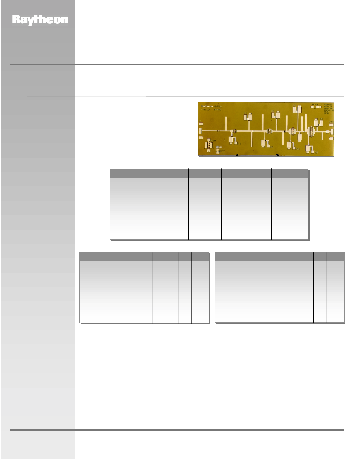
The RMDA1840 is a 4-stage GaAs MMIC amplifier designed as a 18 to 40 GHz broad band amplifier for use in point
to point radios, point to multi-point communications, LMDS, and other millimeter wave applications. The
RMDA1840 utilizes Raytheon’s 0.25µm power PHEMT process and is sufficiently versatile to serve in a variety of
applications, such as a driver amplifier or a frequency multiplier.
4 mil substrate
Small-signal gain 22 dB (typ.)
Pout 1 dB comp 23 dBm (typ.)
Chip size 4.67 mm x 2.00 mm
Parameter Symbol Value Units
Positive DC voltage (+5 V Typical) Vd +6 Volts
Negative DC voltage Vg -2 Volts
Simultaneous (Vd - Vg) Vdg +8 Volts
Positive DC Current I
RF Input Power (from 50 Ω source) P
Operating Baseplate Temperature T
Storage Temperature Range T
Thermal Resistance R
(Channel to Backside)
D
IN
C
stg
JC
442 mA
+15 dBm
-30 to +85 °C
-55 to +125 °C
53 °C/W
Electrical
Characteristics
(At 25°C),
Ω system,
50
Vd = +5 V,
Quiescent
Current
Idq = 400 mA
Parameter Min Typ Max Unit
Frequency Range 18 40 GHz
Gate Supply Voltage (Vg)
Gain Small Signal at
Pin = -5 dBm 20 22 dB
Gain Variation vs
Frequency +/-2.5 dB
Gain at 1dB Compression 21 dB
Power Output at 1 dB
Compression 23 dBm
Notes:
1. Typical range of gate voltage is -1.0 to 0 V to set Idq of 400 mA.
Characteristic performance data and specifications are subject to change without notice.
1
-0.2 V
Parameter Min Typ Max Unit
Power Output Saturated:
Pin = +3 dBm 21 24 dBm
Power Added Efficiency
(PAE): at P1dB 15 %
Input Return Loss
(Pin = -5 dBm) 8 dB
Output Return Loss
(Pin = -5 dBm) 10 dB
www.raytheon.com/micro
Revised January 15, 2001
Page 1
Raytheon RF Components
362 Lowell Street
Andover, MA 01810
Page 2
RMDA1840
18-40 GHz Broad Band Driver Amplifier
Application
Information
Recommended
Procedure
for Biasing and
Operation
MMIC
CAUTION: THIS IS AN ESD SENSITIVE DEVICE.
Chip carrier material should be selected to have GaAs compatible thermal coefficient of expansion and high thermal
conductivity such as copper molybdenum or copper tungsten. The chip carrier should be machined, finished flat,
plated with gold over nickel and should be capable of withstanding 325°C for 15 minutes.
Die attachment should utilize Gold/Tin (80/20) eutectic alloy solder and should avoid hydrogen environment for
PHEMT devices. Note that the backside of the chip is gold plated and is used as RF ground.
These GaAs devices should be handled with care and stored in dry nitrogen environment to prevent contamination
of bonding surfaces. These are ESD sensitive devices and should be handled with appropriate precaution including
the use of wrist grounding straps. All die attach and wire/ribbon bond equipment must be well grounded to prevent
static discharges through the device.
Recommended wire bonding uses 3 mils wide and 0.5 mil thick gold ribbon with lengths as short as practical
allowing for appropriate stress relief. The RF input and output bonds should be typically 0.012” long corresponding
to a typically 2 mil between the chip and the substrate material.
CAUTION: THIS IS AN ESD SENSITIVE DEVICE.
CAUTION: LOSS OF GATE VOLTAGES (Vg) WHILE DRAIN VOLTAGES (Vd) IS PRESENT MAY DAMAGE THE
AMPLIFIER CHIP.
The following sequence of steps must be followed to properly test the amplifier.
Step 1: Turn off RF input power.
Step 2: Connect the DC supply grounds to the grounds
of the chip carrier. Slowly apply negative gate
bias supply voltage of -1.5 V to Vg.
Step 3: Slowly apply positive drain bias supply voltage
of +5 V to Vd.
Step 4: Adjust gate bias voltage to set the quiescent
current of Idq = 400 mA.
Step 5: After the bias condition is established, RF input
signal may now be applied at the appropriate
frequency band.
Step 6: Follow turn-off sequence of:
(i) Turn off RF input power,
(ii) Turn down and off drain voltage (Vd),
(iii) Turn down and off gate bias voltage (Vg).
PRODUCT INFORMATION
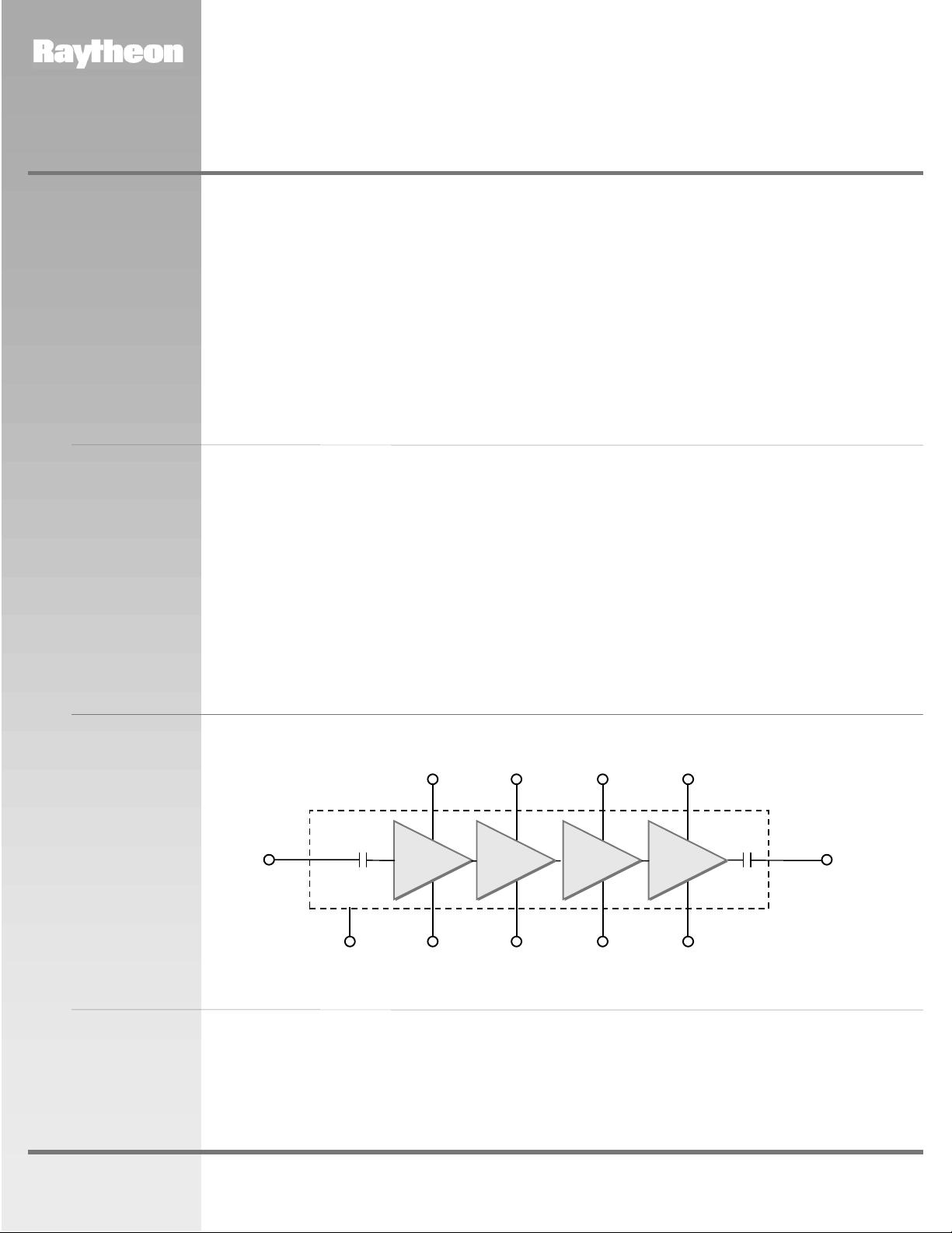
Figure 1
Functional Block
Diagram
www.raytheon.com/micro
Drain Supply
Vd1
MMIC Chip
RF IN
Ground
Back of Chip
Characteristic performance data and specifications are subject to change without notice.
Revised January 15, 2001
Page 2
Gate Supply
Vg1
Drain Supply
Vd2
Gate Supply
Vg2
Drain Supply
Vd3
Gate Supply
Vg3
Drain Supply
Vd4
RF OUT
Gate Supply
Vg4
Raytheon RF Components
362 Lowell Street
Andover, MA 01810
Page 3
RMDA1840
18-40 GHz Broad Band Driver Amplifier
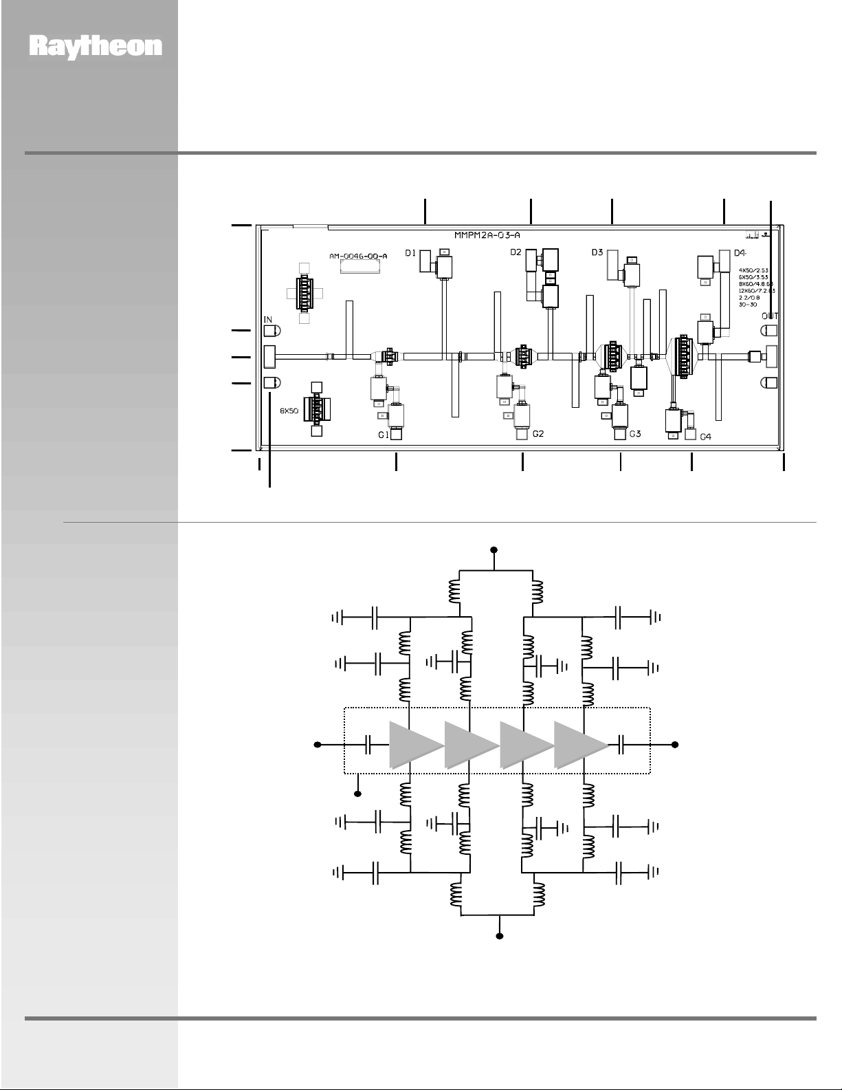
Figure 2
Chip Layout and Bond
Pad Locations
Chip Size is 4.67 mm x
2.0 mm x 100
µm. Back
of chip is RF and DC
ground
MMIC
Dimensions in mm
2.00
1.06
0.83
0.60
0.0
0.0
0.11
1.23
1.50
PRODUCT INFORMATION
2.44 3.16 4.15 4.57
2.35 3.22 3.84
4.67
Figure 3
Recommended
Application Schematic
Circuit Diagram
RF IN
Ground
(Back of Chip)
10,000pF
100pF
MMIC Chip
100pF
10,000pF
Drain Supply
Vd = +5 V
L
L
LLLL
L
L
100pF
LL
100pF
L
Gate Supply
Vg
L = Bond Wire Inductance
L
L
100pF
LL
100pF
L
L
10,000pF
L
100pF
L
100pF
L
10,000pF
RF OUT
www.raytheon.com/micro
Note: For output power level detection, bias both detector and reference diodes. DC voltage difference between detector and reference can be used
to measure output power after calibration. If output power level detection is not desired, do not make connection to detector bond pad.
Characteristic performance data and specifications are subject to change without notice.
Revised January 15, 2001
Page 3
Raytheon RF Components
362 Lowell Street
Andover, MA 01810
Page 4
RMDA1840
18-40 GHz Broad Band Driver Amplifier
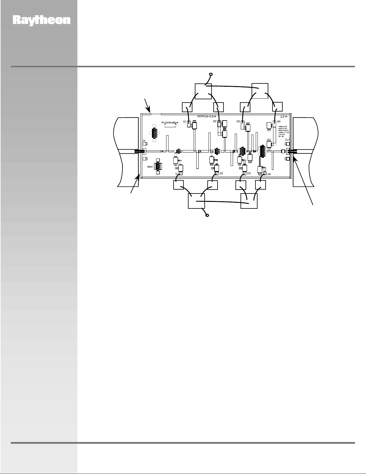
Figure 4
Recommended
Assembly Diagram
MMIC
10,000pF
Die-Attach
80Au/20Sn
5mil Thick
Alumina
50-Ohm
RF
Input
100pF 100pF 100pF100pF
2 mil Gap
10,000pF 10,000pF
Note Use 0.003” by 0.0005” Gold Ribbon for bonding. RF input and output bonds should be less than 0.015” long with stress relief. If output
power level detection is not desired, do not make connection to detector bond pad.
Vd (Positive)
10,000pF
100pF100pF 100pF 100pF
Vg (Negative)
PRODUCT INFORMATION
5 mil
Thick
Alumina
50-Ohm
RF
Output
L< 0.015”
(4 Places)
www.raytheon.com/micro
Characteristic performance data and specifications are subject to change without notice.
Revised January 15, 2001
Page 4
Raytheon RF Components
362 Lowell Street
Andover, MA 01810
Page 5
RMDA1840
18-40 GHz Broad Band Driver Amplifier
Performance
Data
MMIC
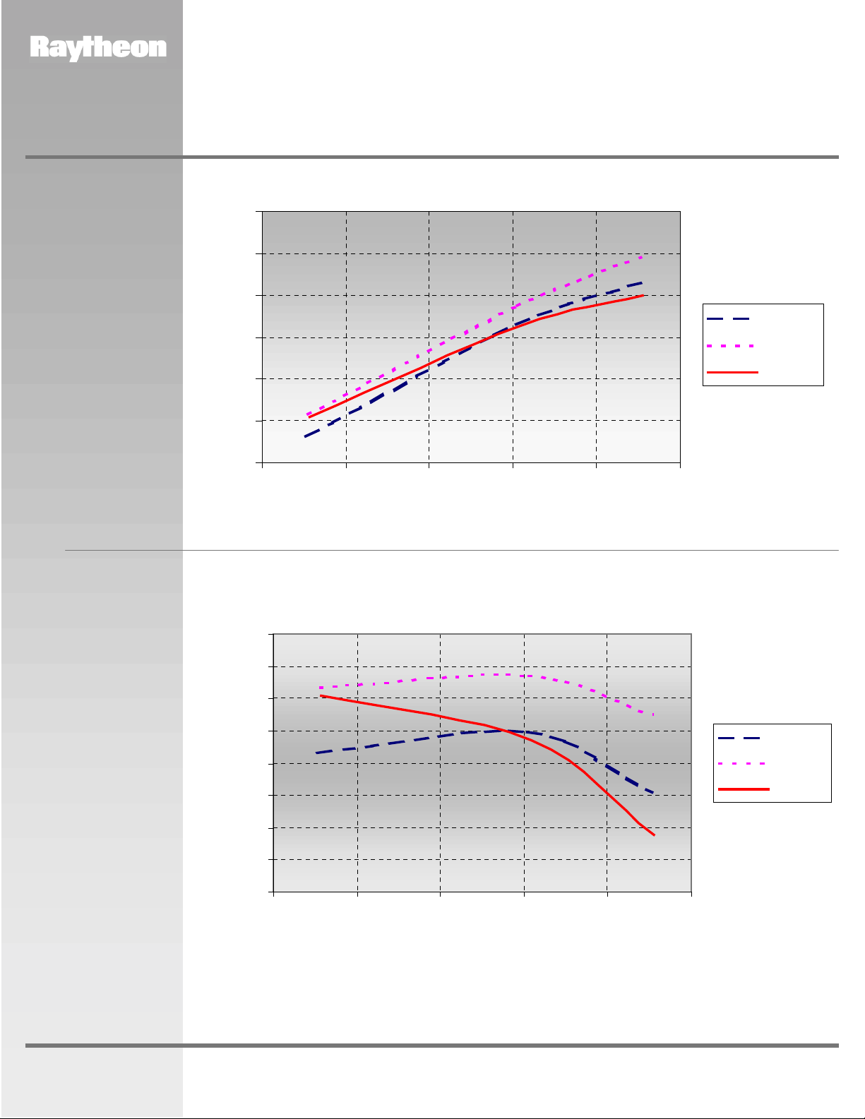
27
25
23
21
Pout (dBm)
19
17
15
-6 -4 -2 0 2 4
PRODUCT INFORMATION
Pout vs. Pin
Vd = 5V, Id = 400mA
18 GHz
29 GHz
40 GHz
Pin (dBm)
23
22.5
22
21.5
21
20.5
Gain (dB)
20
19.5
19
-6 -4 -2 0 2 4
Gain vs. Pin
Vd = 5V, Id = 400mA
18 GHz
29 GHz
40 GHz
Pin (dBm)
www.raytheon.com/micro
Characteristic performance data and specifications are subject to change without notice.
Revised January 15, 2001
Page 5
Raytheon RF Components
362 Lowell Street
Andover, MA 01810
Page 6
m
)
RMDA1840
18-40 GHz Broad Band Driver Amplifier
Performance
Data
MMIC
30
28
26
24
22
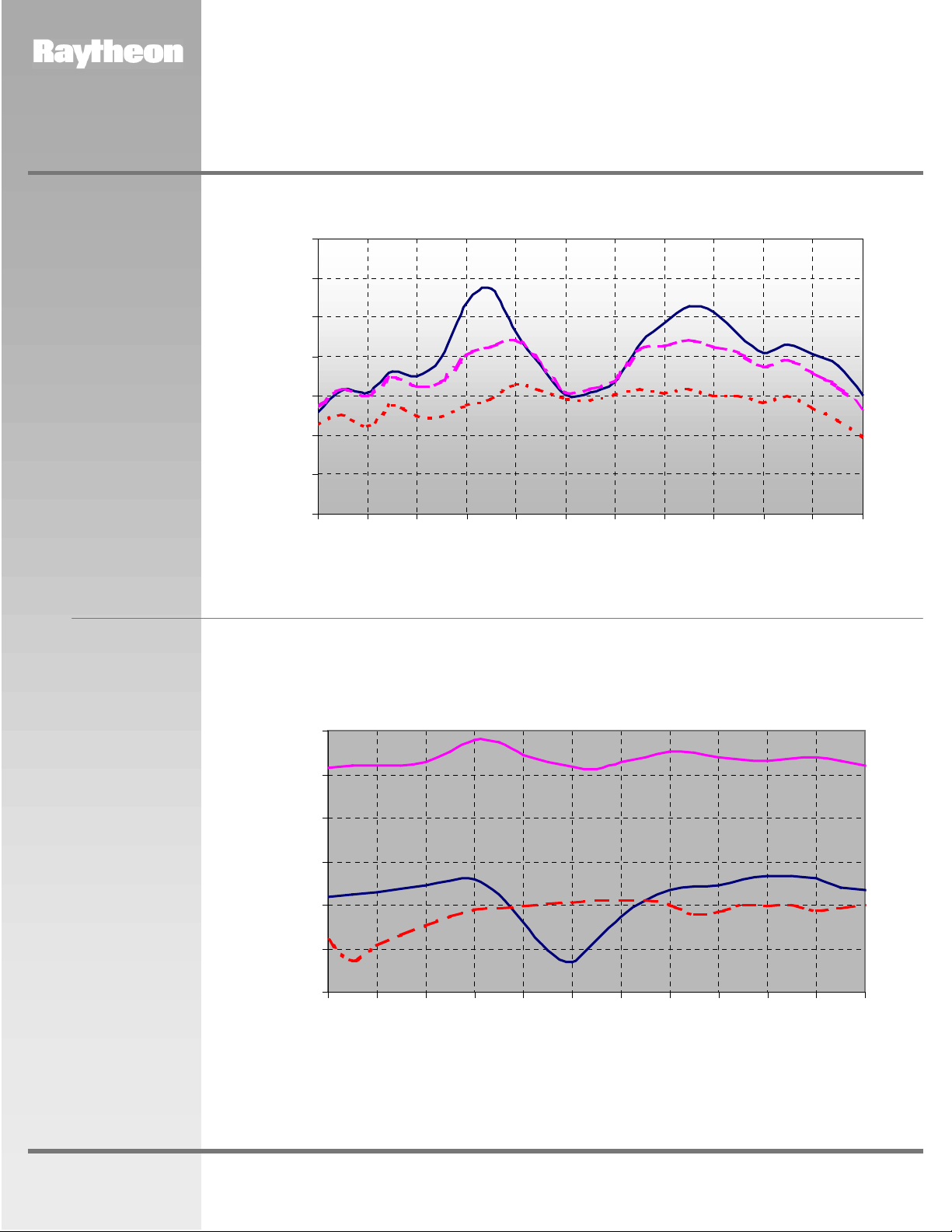
Gain (dB)
20
Power Out (dBm)
18
16
PRODUCT INFORMATION
Gain vs. Frequency
Power In = -5, 0, +5 dBm Vd = 5V, Id = 400mA
Pin = -5 dBm
Pin = 0 dBm
Pin = +5 dB
18 20 22 24 26 28 30 32 34 36 38 40
Frequency (GHz)
S21, S11, S22 Mag
vs. Frequency Vd = 5V, Id = 400mA
30
S21
20
10
0
-10
S21, S11, S22 Mag (dB
-20
-30
18 20 22 24 26 28 30 32 34 36 38 40
Characteristic performance data and specifications are subject to change without notice.
S11
S22
Frequency (GHz)
www.raytheon.com/micro
Revised January 15, 2001
Page 6
Raytheon RF Components
362 Lowell Street
Andover, MA 01810
Page 7
Worldwide Sales
Representatives
PRODUCT INFORMATION
North
America
Europe
Asia
D&L Technical Sales
6139 S. Rural Road, #102
Tempe, AZ 85283
480-730-9553
fax: 480-730-9647
Nicholas Delvecchio, Jr.
[email protected]
Hi-Peak Technical Sales
P.O. Box 6067
Amherst, NH 03031
866-230-5453
fax: 603-672-9228
sales@hi–peak.com
Sangus OY
Lunkintie 21,
90460 Oulunsalo
Finland
358-8-8251-100
fax: 358-8-8251-110
Juha Virtala
[email protected]
ITX Corporation
2–5, Kasumigaseki
3–Chome
Chiyoda–Ku
Tokyo 100-6014 Japan
81-3-4288-7073
fax: 81-3-4288-7243
Maekawa Ryosuke
maekawa.ryosuke@
itx–corp.co.jp
Spartech South
2115 Palm Bay Road, NE,
Suite 4
Palm Bay, FL 32904
321-727-8045
fax: 321-727-8086
Jim Morris
[email protected]
Sangus AB
Berghamnvagen 68
Box 5004
S–165 10 Hasselby
Sweden
Ronny Gustafson
468-0-380210
fax: 468-0-3720954
Sea Union
9F-1, Building A, No 19-3
San-Chung Road
Nankang Software Park
Taiwan, ROC
Taipei 115
02-2655-3989
fax: 02-2655-3918
Murphy Su
[email protected]
TEQ Sales, Inc.
920 Davis Road, Suite 304
Elgin, IL 60123
847-742-3767
fax: 847-742-3947
Dennis Culpepper
[email protected]
Globes Elektronik & Co.
Klarastrabe 12
74072 Heilbronn
Germany
49-7131-7810-0
fax: 49-7131-7810-20
Ulrich Blievernicht
[email protected]
Cantec Representatives
8 Strathearn Ave, No. 18
Brampton, Ontario
Canada L6T 4L9
905-791-5922
fax: 905-791-7940
Dave Batten
[email protected]
MTI Engineering Ltd.
Afek Industrial Park
Hamelacha 11
New Industrial Area
Rosh Hayin 48091
Israel
972-3-902-5555
fax: 972-3-902-5556
Adi Peleg
[email protected]
Steward Technology
6990 Village Pkwy #206
Dublin, CA 94568
925-833-7978
fax: 925-560-6522
John Steward
Sirces srl
Via C. Boncompagni, 3B
20139 Milano
Italy
3902-57404785
fax: 3902-57409243
Nicola Iacovino
Worldwide
Distribution
Sales Office
Headquarters
Customer
Support
www.raytheon.com/micro
Headquarters
6321 San Ignacio Drive
San Jose, CA 95119
408-360-4073
fax: 408-281-8802
Art Herbig
[email protected]
Belgium and Luxembourg
Cipalstraat
2440 GEEL
Belgium
32 14 570670
fax: 32 14 570679
[email protected]
United States
(East Coast)
Raytheon
362 Lowell Street
Andover, MA 01810
978-684-8628
fax: 978-684-8646
Walter Shelmet
wshelmet@
rrfc.raytheon.com
Characteristic performance data and specifications are subject to change without notice.
Revised January 15, 2001
Page 7
United Kingdom
Burnt Ash Road
Aylesford, Kent
England
ME207XB
44 1622882467
fax: 44 1622882469
rfsales.uk@
bfioptilas.avnet.com
United States
(West Coast)
Raytheon
362 Lowell Street
Andover, MA 01810
978-684-8919
fax: 978-684-8646
Rob Sinclair
robert_w_sinclair@
rrfc.raytheon.com
France
4 Allee du Cantal
Evry, Cedex
France
33 16079 5900
fax: 33 16079 8903
sales.fr@
bfioptilas.avnet.com
Europe
Raytheon
AM Teckenberg 53
40883 Ratingen
Germany
49-2102-706-155
fax: 49-2102-706-156
Peter Hales
peter_j_hales@
raytheon.com
Holland
Chr. Huygensweg 17
2400 AJ ALPHEN AAN DEN
RIJN
The Netherlands
31 172 446060
fax: 33 172 443414
sales.nl@
bfioptilas.avnet.com
Asia
Raytheon
Room 601, Gook Je Ctr. Bldg
191 Hangang Ro 2-GA
Yongsan-Gu, Seoul,
Korea 140-702
82-2-796-5797
fax: 82-2-796-5790
T.G. Lee
tg_lee@
rrfc.raytheon.com
Spain
C/Isobel Colbrand, 6 – 4a
28050 Madrid
Spain
34 913588611
fax: 34 913589271
sales.es@
bfioptilas.avnet.com
Raytheon RF Components
362 Lowell Street
Andover, MA 01810
 Loading...