

Page 1
RM912
CDMA/AMPS 3–4 Volt Power Amplifier (824–849 MHz)
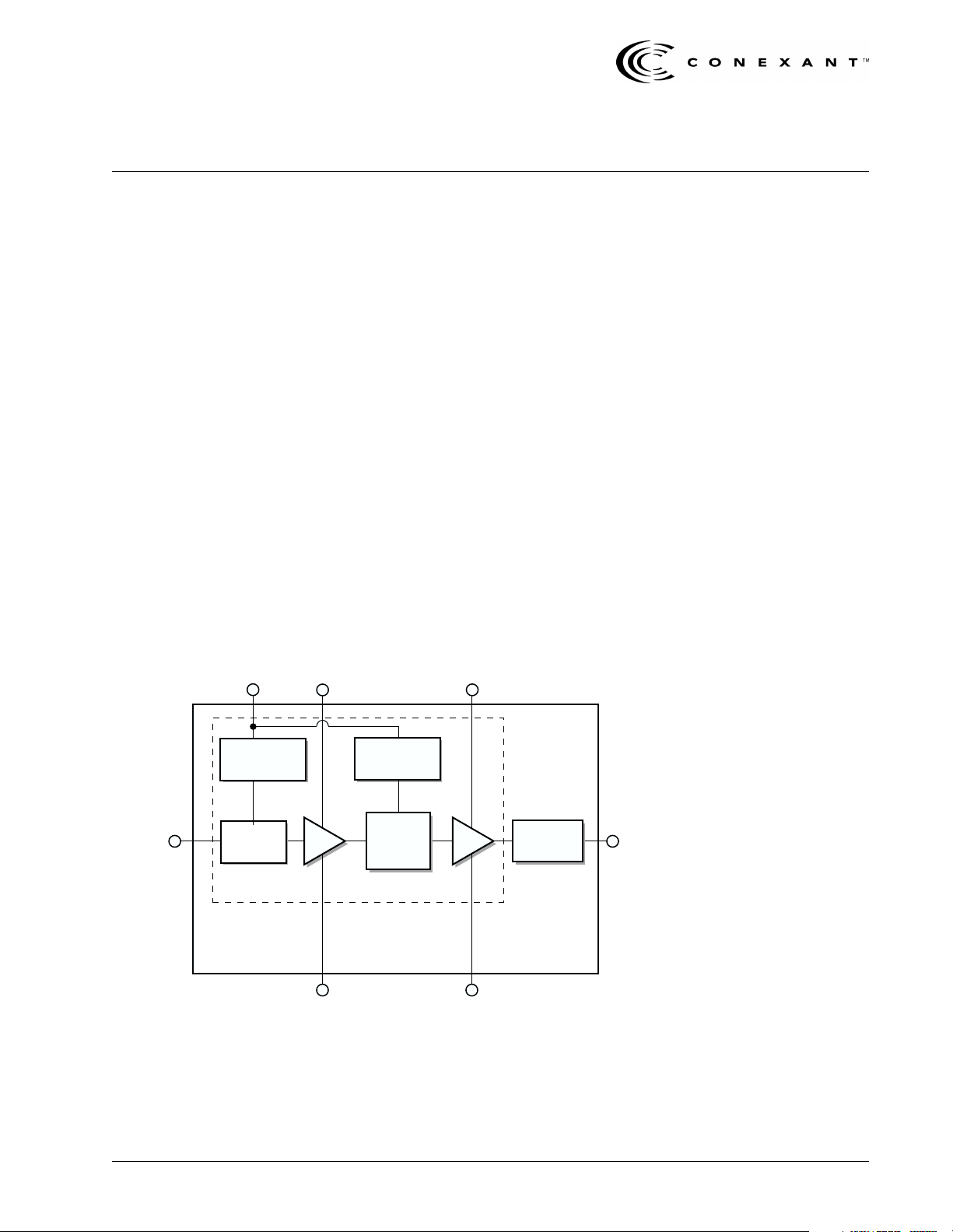
The RM912 dual mode Code Division Multiple Access (CDMA)/Advanced Mobile
Phone Service (AMPS) Power Amplifier is a fully matched 6-pin LCC surface mount
module designed for mobile units operating in the 824-849 MHz cellular bandwidth.
This device meets stringent IS95 CDMA linearity requirements to beyond 28 dBm
output power and can be driven to power output levels beyond 31 dBm for high
efficiency FM mode operation. A single GaAs Microwave Monolithic Intergrated
Circuit (MMIC) contains all active circuitry in the module. The MMIC contains
on-board bias circuitry, as well as input and interstage matching circuits. The output
match is realized off-chip within the module package to optimize efficiency and power
performance into a 50
process that provides for all positive voltage DC supply operation while maintaining
high efficiency and good linearity. Primary bias to the RM912 can be supplied directly
from a three cell nickel-cadmium, single cell lithium-ion, or other suitable battery with
output in the 3-4 volt range. Power down is accomplished by setting the voltage on
the low current reference pin to zero volts. No external supply side switch is needed
as typical “off” leakage is a few microamperes with full primary voltage supplied from
the battery.
Ω load. This device is manufactured with Conexant’s GaAs HBT
Functional Block Diagram
VREF
(3)
VCC1
(1) (4)
VCC2
Distinguishing Features
• Low voltage positive bias supply
• Good linearity
• High efficiency
• Dual mode operation
• Large dynamic range
• 6-pin LCC package
(6 x 6 x 1.5 mm)
• Power down control
Applications
• Digital cellular (CDMA)
• Analog cellular (AMPS)
• Wireless local loop
Driver
Stage Bias
RF
Input
(2) (5)
Data Sheet 100635G
2000, Conexant Systems, Inc. All Rights Reserved. August 2000
Input
Match
DA
GND GND
(6, 7)
MMIC
Power
Stage Bias
Inter
Stage
Match
PA
(6, 7)
Output
Match
MODULE
RF
Output
Page 2
Electrical Specifications RM912
CDMA/AMPS 3–4 Volt Power Amplifier (824–849 MHz)
Electrical Specifications
The following tables list the electrical characteristics of the RM912 Power Amplifier. Table 1 lists
the absolute maximum rating for continuous operation. Table 2 lists the recommended operating
conditions for achieving the electrical performance listed in Table 3. Tab l e 3 lists the electrical
performance of the RM912 Power Amplifier over the recommended operating conditions.
Table 1. Absolute Maximum Ratings
Parameter Symbol Min Nominal Max Unit
RF Input Power Pin — 3.0 6.0 dBm
Supply Voltage Vcc — 3.4 5.0 Volts
Reference Voltage Vref — 3.0 3.3 Volts
Case Operating Temperature Tc –30 25 +110 °C
Storage Temperature Tstg –55 — +125 °C
NOTE(S):
(1)
No damage assuming only one parameter is set at limit at a time with all other parameters set at or below nominal value.
Table 2. Recommended Operating Conditions
Parameter Symbol Min Nominal Max Unit
(1)
Supply Voltage Vcc 3.2 3.4 4.2 Volts
Reference Voltage Vref 2.9 3.0 3.1 Volts
Operating Frequency Fo 824.0 836.5 849.0 MHz
Operating Temperature To –30 +25 +85 °C
2 Conexant 100635G
Page 3
RM912 Electrical Specifications
CDMA/AMPS 3–4 Volt Power Amplifier (824–849 MHz)
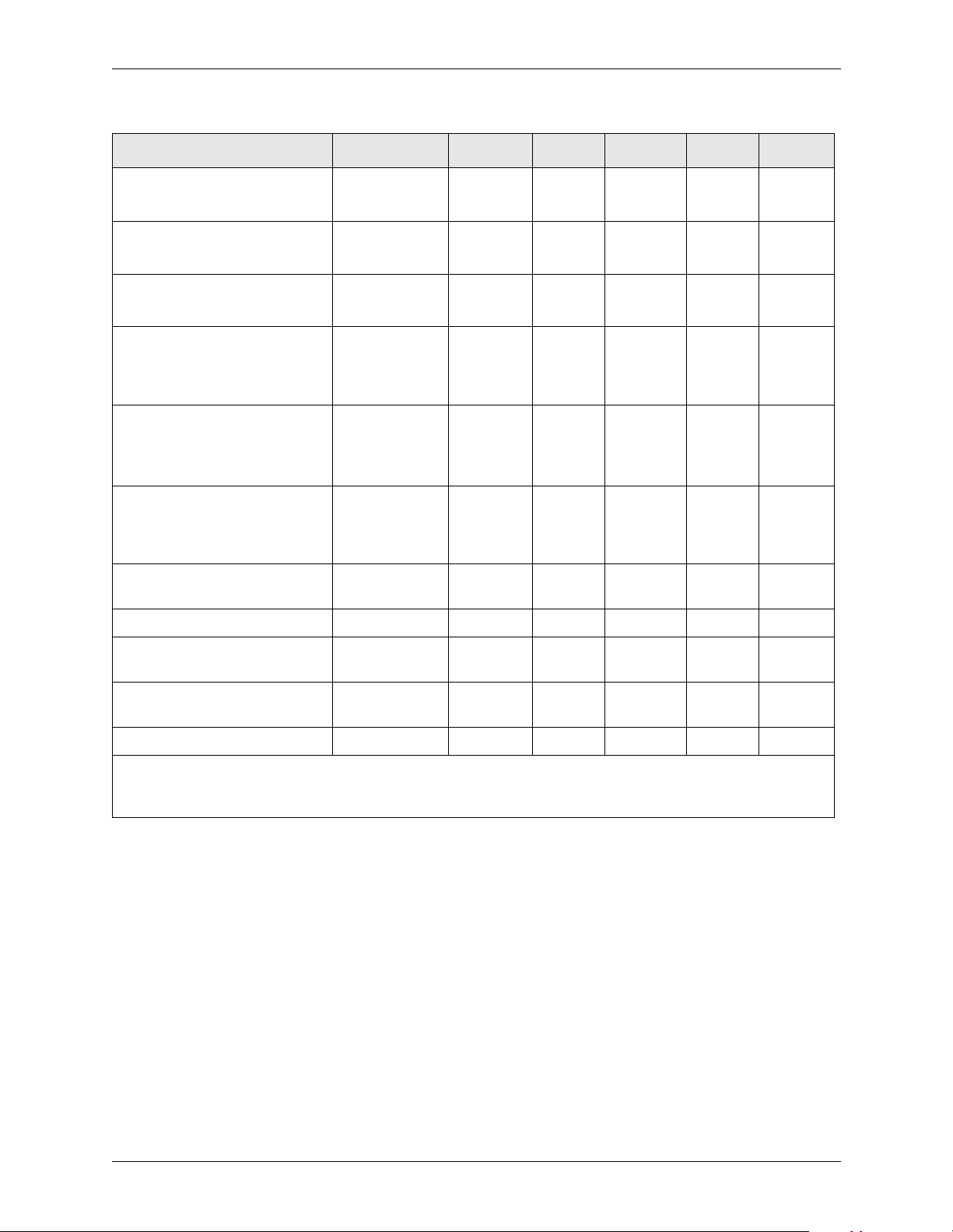
Table 3. Electrical Specifications for CDMA / AMPS Nominal Operating Conditions
Characteristics Condition Symbol Min Typical Max Unit
Quiescent current Vref = 3.0
Vref = 2.9
Gain–Digital Po = 0 dBm
Po = 28 dBm
Gain–Analog Po = 0 dBm
Po = 31 dBm
Iq
Iq
G
G
G
Gp
—
—
26.0
p
27.0
26.0
26.0
100.0
80.0
28.0
29.0
28.0
28.0
Power Added Efficiency
– Analog Mode
– Digital Mode
Adjacent Channel Power
– 885 kHz Offset
–1980 kHz Offset
(2)
Po = 31 dBm
Po = 28 dBm
Po ≤ 28 dBm
Po ≤ 28 dBm
PA Ea
PA Ed
ACP1
ACP2
43.0
32.0
—
—
45.0
34.0
–50.0
–58.0
Harmonic Suppression
– Second
– Third
Po ≤ 31 dBm
Po ≤ 31 dBm
AFo2
AFo3
—
—
–42.0
–45.0
(1)
—
—
—
—
—
—
—
—
–48.0
–56.0
–30.0
–30.0
mA
mA
dB
dB
dB
dB
%
%
dBc
dBc
dBc
dBc
Noise Power in RX Band
Po @ 28 dBm RxBN —–134.0 –133.0 dBm/Hz
869-894 MHz
Noise Figure — NF — 6.0 — dB
Input Voltage Standing Wave
— VSWR — 1.4:1 ——
Ratio
Stability (Spurious output) 5:1 VSWR
S ——–60.0 dBc
All phases
Ruggedness – No damage Po ≤ 31 dBm Ru 10:1 ——VSWR
NOTE(S):
(1)
Vcc = +3.4 V, Vref = +3.0 V, Freq = 836.5 MHz, Tc = 25 °C, unless otherwise specified.
(2)
ACP is specified per IS95 as the ratio of the total in-band power (1.23 MHz BW) to adjacent power in a 30 kHz BW.
100635G Conexant 3
Page 4
Electrical Specifications RM912
CDMA/AMPS 3–4 Volt Power Amplifier (824–849 MHz)
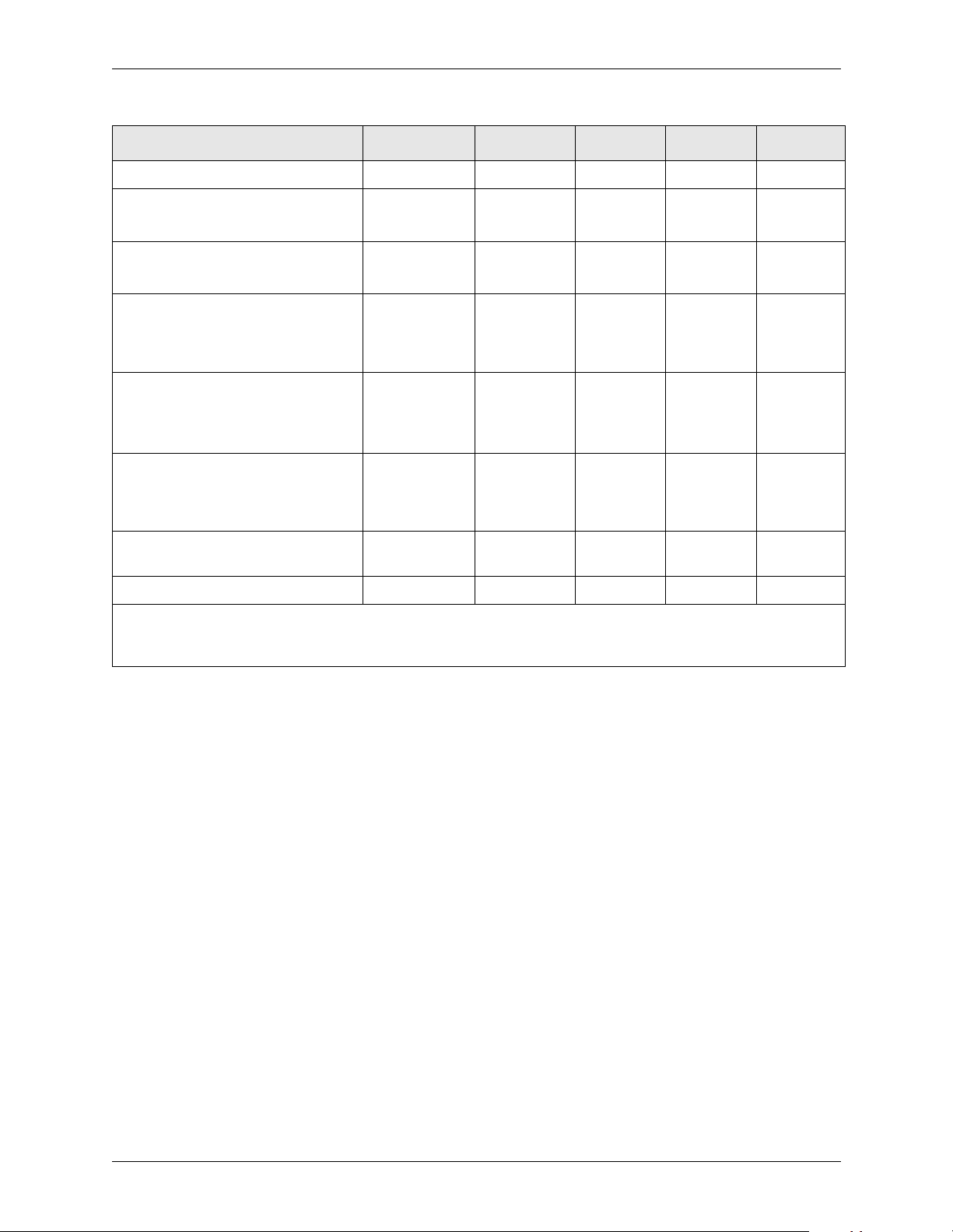
Table 4. Electrical Specifications Limits for CDMA / AMPS Recommended Operating Conditions
Characteristics Condition Symbol Min Max Unit
Quiescent current Vref = 3.0 Iq — 140.0 mA
Gain–Digital Po = 0 dBm
Po = 28 dBm
Gain–Analog Po = 0 dBm
Po = 31dBm
Power Added Efficiency
– Analog Mode
– Digital Mode
Adjacent Channel Power
– 885 kHz Offset
–1980 kHz Offset
Harmonic Suppression
Noise Power in RX Band
869—894 MHz
(2)
– Second
– Third
Po = 31 dBm
Po = 28 dBm
Po ≤ 28 dBm
Po ≤ 28 dBm
Po ≤ 31 dBm
Po ≤ 31 dBm
Po @ 28 dBm RxBN —–131.0 dBm/Hz
G
G
p
G
Gp
PAEa
PAEd
ACP1
ACP2
AFo2
AFo3
25.0
25.0
25.0
24.0
42.0
32.0
—
—
—
—
29.0
32.0
29.0
32.0
—
—
–44.0
–56.0
–40.0
–40.0
(1)
dB
dB
dB
dB
%
%
dBc
dBc
dBc
dBc
Input Voltage Standing Wave Ratio — VSWR — 2:1 —
NOTE(S):
(1)
Per Tab le 2 .
(2)
ACP is specified per IS95 as the ratio of the total in-band power (1.23 MHz BW) to adjacent power in a 30 kHz BW.
4 Conexant 100635G
Page 5
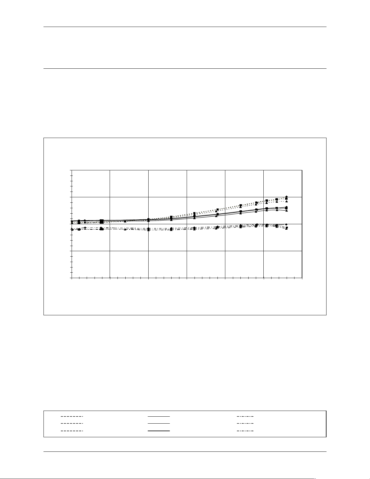
RM912 Characterization Data
CDMA/AMPS 3–4 Volt Power Amplifier (824–849 MHz)
Characterization Data
The following charts illustrate the characteristics of a typical RM912 Power Amplifier tested in the
evaluation board described in the following section. The amplifier was selected by characterizing a
group of devices and choosing a part with average electrical performance at both nominal and
worst case (limit) conditions. Figures 1 through 4 illustrate the digital signal characteristics and
Figures 5 through 8 illustrate the analog characteristics of the RM912.
Figure 1. Digital Gain vs. Output Power
Vref = 3.0V, Vcc = 3.4V
32.50
30.00
27.50
Gain (dB)
25.00
22.50
0.00 5.00 10.00 15.00 20.00 25.00 30.00
Output Power (dBm)
Legend
◆
■
▲
824 MHz @ –30 °C
837 MHz @ –30 °C
849 MHz @ –30 °C
◆
■
▲
100635G Conexant 5
824 MHz @ +25 °C
837 MHz @ +25 °C
849 MHz @ +25 °C
◆
■
▲
824 MHz @ +85 °C
837 MHz @ +85 °C
849 MHz @ +85 °C
Page 6
Characterization Data RM912
CDMA/AMPS 3–4 Volt Power Amplifier (824–849 MHz)
Figure 2. Digital Adjacent Channel Power Magnitude (ACP1) vs. Output Power
Vref = 3.0V, Vcc = 3.4V, 885 kHz Off set
80.00
70.00
60.00
50.00
| ACP1 (dBc) |
40.00
30.00
20.00
0.00 5.00 10.00 15.00 20.00 25.00 30.00
Output Power (dBm)
Figure 3. Digital Adjacent Channel Power Magnitude (ACP2) vs. Output Power
◆
■
▲
Legend
Vr ef = 3.0V , V c c = 3.4V, 1980 kHz Offset
80.00
70.00
60.00
50.00
| ACP2 (dBc) |
40.00
30.00
20.00
0.00 5.00 10.00 15.00 20.00 25.00 30.00
Output Power (dBm)
◆
■
▲
824 MHz @ –30 °C
837 MHz @ –30 °C
849 MHz @ –30 °C
◆
■
▲
824 MHz @ +25 °C
837 MHz @ +25 °C
849 MHz @ +25 °C
824 MHz @ +85 °C
837 MHz @ +85 °C
849 MHz @ +85 °C
6 Conexant 100635G
Page 7

RM912 Characterization Data
CDMA/AMPS 3–4 Volt Power Amplifier (824–849 MHz)
Figure 4. Digital Power Added Efficiency vs. Output Power
Vref = 3.0V, Vcc = 3.4V
40.00
35.00
30.00
25.00
20.00
DPAE (%)
15.00
10.00
5.00
0.00
0.00 5.00 10.00 15.00 20.00 25.00 30.00
Output Power (dBm)
Figure 5. Analog Gain vs. Output Power
Vref = 3.0V, Vcc = 3.4V
32.50
30.00
27.50
Gain (dB)
25.00
22.50
0.00 5.00 10.00 15.00 20.00 25.00 30.00
Output Power (dBm)
Legend
◆
■
▲
824 MHz @ –30 °C
837 MHz @ –30 °C
849 MHz @ –30 °C
◆
■
▲
100635G Conexant 7
824 MHz @ +25 °C
837 MHz @ +25 °C
849 MHz @ +25 °C
◆
■
▲
824 MHz @ +85 °C
837 MHz @ +85 °C
849 MHz @ +85 °C
Page 8

Characterization Data RM912
CDMA/AMPS 3–4 Volt Power Amplifier (824–849 MHz)
Figure 6. Analog Power Added Efficiency vs. Output Power
Vref = 3.0V, Vcc = 3.4V
50.00
45.00
40.00
35.00
30.00
25.00
PAE (%)
20.00
15.00
10.00
5.00
0.00
0.00 5.00 10.00 15.00 20.00 25.00 30.00
Output Power (dBm)
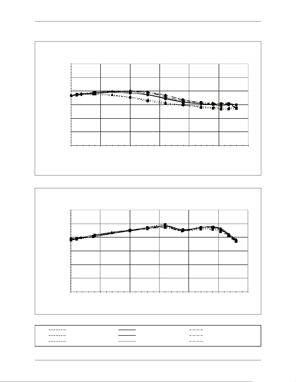
Figure 7. Analog Second Order Harmonic Suppression Magnitude
Vr ef = 3.0V , V c c = 3.4V
70.00
60.00
50.00
40.00
30.00
| AFo2 (dBc) |
20.00
10.00
0.00
10.00 15.00 20.00 25.00 30.00
Output Pow er (dBm)
Legend
◆
■
▲
824 MHz @ –30 °C
837 MHz @ –30 °C
849 MHz @ –30 °C
◆
■
▲
824 MHz @ +25 °C
837 MHz @ +25 °C
849 MHz @ +25 °C
◆
■
▲
824 MHz @ +85 °C
837 MHz @ +85 °C
849 MHz @ +85 °C
8 Conexant 100635G
Page 9

RM912 Characterization Data
CDMA/AMPS 3–4 Volt Power Amplifier (824–849 MHz)
Figure 8. Analog Third Order Harmonic Suppression Magnitude
Vref = 3.0V, Vcc = 3.4V
70.00
60.00
50.00
40.00
30.00
| AFo3 (dBc) |
20.00
10.00
0.00
10.00 15.00 20.00 25.00 30.00
Output Power (dBm)
Legend
◆
■
▲
824 MHz @ –30 °C
837 MHz @ –30 °C
849 MHz @ –30 °C
◆
■
▲
100635G Conexant 9
824 MHz @ +25 °C
837 MHz @ +25 °C
849 MHz @ +25 °C
◆
■
▲
824 MHz @ +85 °C
837 MHz @ +85 °C
849 MHz @ +85 °C
Page 10

Characterization Data RM912
CDMA/AMPS 3–4 Volt Power Amplifier (824–849 MHz)
Figure 9. Digital Gain vs. Output Power
40.00
35.00
30.00
25.00
20.00
15.0 0
10.0 0
5.00
Digital Gain at 28 dBm output power (dB)
0.00
3.20V
-30C
COL D R OOM T EMP E R A T UR E HOT
824 MH z 836.5 MHz 849 MHz
3.40V
-30C
4.20V
-30C
3.20V
25C
Coll ect or Volt age
Case Temperat ure
3.40V
25C
4.20V
25C
3.20V
85C
3.40V
85C
Figure 10. Digital Adjacent Channel Power Magnitude (ACP1) vs. Output Power
4.20V
85C
70.00
60.00
50.00
40.00
30.00
20.00
10.0 0
| ACP1 at 28 dBm Output Power (dBc) |
0.00
3.20V
-30C
COL D R OOM T EMP E R A T UR E HOT
824 MH z 836.5 MHz 849 MHz
3.40V
-30C
4.20V
-30C
3.20V
25C
Collector Voltage
C as e T emper at ur e
3.40V
25C
4.20V
25C
3.20V
85C
3.40V
85C
4.20V
85C
10 Conexant 100635G
Page 11

RM912 Characterization Data
CDMA/AMPS 3–4 Volt Power Amplifier (824–849 MHz)
Figure 11. Digital Adjacent Channel Power Magnitude (ACP2) vs. Output Power
80.00
70.00
60.00
50.00
40.00
30.00
20.00
10.00
| ACP2 at 28 dBm Output Power (dBc) |
0.00
3.20V
-30C
COL D R OOM T EMP E R A T UR E HOT
824 MHz 836.5 MHz 849 MHz
3.40V
-30C
4.20V
-30C
3.20V
25C
3.40V
25C
4.20V
25C
3.20V
85C
Coll ector V o lt age
Case T emperatur e
3.40V
85C
4.20V
85C
Figure 12. Analog Gain vs. Output Power
40.00
35.00
30.00
25.00
20.00
15.00
10.00
5.00
0.00
Analog Gain at 31 dBm Output Power (dB)
3.20V
-30C
COL D R OOM T E M P E R AT U R E H OT
3.40V
-30C
4.20V
-30C
824 MHz 836.5 MHz 849 MH z
3.20V
25C
3.40V
25C
4.20V
25C
Collector V olt age
C as e T emper at ur e
3.20V
85C
3.40V
85C
4.20V
85C
100635G Conexant 11
Page 12

Characterization Data RM912
CDMA/AMPS 3–4 Volt Power Amplifier (824–849 MHz)
Figure 13. Analog Second Order Harmonic Suppression Magnitude
70.00
60.00
50.00
40.00
30.00
20.00
10.00
| AFo2 at 31 dBm Output Power (dBc) |
0.00
3.20V
-30C
COLD
3.40V
-30C
4.20V
-30C
RO OM TEM PE RA TURE HOT
824 MH z 836.5 MHz 849 MHz
3.20V
25C
3.40V
25C
Collector Voltage
Case T emper ature
4.20V
25C
Figure 14. Analog Third Order Harmonic Suppression Magnitude
3.20V
85C
3.40V
85C
4.20V
85C
| AFo3 at 31 dBm Output Power (dBc) |
70.00
60.00
50.00
40.00
30.00
20.00
10.00
0.00
3.20V
-30C
COLD
3.40V
-30C
4.20V
-30C
RO OM TEMPERATURE
824 MH z 836.5 MHz 849 MHz
3.20V
25C
3.40V
25C
Coll ect or V ol t age
Case T emperatur e
4.20V
25C
3.20V
85C
HO T
3.40V
85C
4.20V
85C
12 Conexant 100635G
Page 13

RM912 Characterization Data
CDMA/AMPS 3–4 Volt Power Amplifier (824–849 MHz)
Figure 15. Noise Figure Variation Over Recommended Operating Conditions
10.0 0
9.00
8.00
7.00
6.00
5.00
4.00
3.00
Noise Figure (dB)
2.00
1.0 0
0.00
3.20V
-30C
COLD
3.40V
-30C
4.20V
-30C
RO OM TEM PE RATURE HOT
824 MHz 836.5 MHz 849 MH z
3.20V
25C
3.40V
25C
4.20V
25C
Collector V oltage
Case T emperature
3.20V
85C
3.40V
85C
4.20V
85C
Figure 16. Voltage Standing Wave Ratio Variation Over Recommended Operating Conditions
2.00
1.80
1.60
1.40
1.20
1.00
0.80
VSWR (:1)
0.60
0.40
0.20
0.00
3.20V
-30C
COLD R OOM T E MP E R AT U R E H OT
824 MHz 836.5 MH z 849 MHz
3.40V
-30C
4.20V
-30C
3.20V
25C
3.40V
25C
4.20V
25C
3.20V
85C
Collector Volt age
Case Temperature
3.40V
85C
4.20V
85C
100635G Conexant 13
Page 14

Evaluation Board Description RM912
CDMA/AMPS 3–4 Volt Power Amplifier (824–849 MHz)
Evaluation Board Description
The evaluation board is a platform for testing and interfacing design circuitry. To accommodate the
interface testing of the RM912, the evaluation board schematic and diagrams are included for
preliminary analysis and design. Figure 17 shows the basic schematic of the board for the 824 MHz
to 849 MHz range. Figure 18 illustrates the board layout.
Figure 17. Evaluation Board Schematic
GND
RFOUT
VCC2
RFIN
Vref
C1
1
VCC1
2
RFIN
VREF
3
Figure 18. Evaluation Board Assembly Diagram
6
5
4
C2
RFOUT
C3 C4
Vcc
100635_003
REF
DESIGNATIONS
C1
C2
C3
C4
VALUES QTY
100 pF
4.7 uF
39 pF
1000 pF 1
1
1
1
100635_004
14 Conexant 100635G
Page 15

RM912 Package Dimensions and Pin Descriptions
CDMA/AMPS 3–4 Volt Power Amplifier (824–849 MHz)
Package Dimensions and Pin Descriptions
The RM912 is a multi-layer laminate base, overmold encapsulated modular package designed for
surface mount solder attachment to a printed circuit board.
Figure 19. RM912 Package Drawing
PIN 1
PIN 2
PIN 3
5.92/6.15
[.2333/.242]
PIN 6
PIN 5
PIN 4
5.92/6.15
[.2333/.242]
1.500 [.060]
TYP
2.500
[.0098]
(4x)
(PIN 1)
PIN 7
2.870 [.113]
(2x)
1.981 [.078]
(2x)
COPPER
BOTTOM
1.219 [.048]
(2x)
2.006 [.079
2.500
[.0098]
(4x)
.762 [.030]
6x
R .500 TYP
[R .020 TYP]
2.870 [.113]
(4x)
1.854 [.073]
(6x)
1.245 [.049]
(2x)
(4X)
1.016 [.040]
SOLDER MASK
BOTTOM
100635_002
100635G Conexant 15
Page 16

Package Dimensions and Pin Descriptions RM912
CDMA/AMPS 3–4 Volt Power Amplifier (824–849 MHz)
Table 5. Pin Description
Pin # Function
1
2 RF Input
3VREF
4
5RF Output
6GND
7
NOTE(S):
(1)
All supply pins may be connected together at the supply.
(2)
Package underside is GND.
Figure 20. Typical Case Markings
Mark Pin 1
Identifier
VCC1
VCC2
GND
(1)
(1)
(2)
CONEXANT
RM912-11
NXXXXX.XX
YYWW MEX
YY = Manufacture Year
WW = Week Package
MEX = Country Code
16 Conexant 100635G
Manufacturing
Part Number - Revision
Lot
Number
Sealed
100635_006
Page 17

RM912 Package Dimensions and Pin Descriptions
CDMA/AMPS 3–4 Volt Power Amplifier (824–849 MHz)
Production quantities of this product are shipped in the standard tape-and-reel format illustrated
below.
Figure 21. 6 x 6 Tape and Reel
8.00 ± .10
PIN 1
4.00 ± .10
0.292 ± .02
1.50 ± .10
1.50 ± .25
1.75 ± .10
5.50 ± .10
12.00
+.30
-.10
8˚ MAX 7˚ MAX
6.35 ± .10
0 0 0
AK B
3M Carrier Tape
1.59 ± .10
6.35 ± .10
100635_005
100635G Conexant 17
Page 18

Electrostatic Discharge Sensitivity RM912
CDMA/AMPS 3–4 Volt Power Amplifier (824–849 MHz)
Electrostatic Discharge Sensitivity
The RM912 is a Class I device. Figure 22 lists the Electrostatic Discharge (ESD) immunity level
for each pin of the RM912 product. The numbers in Figure 22 specify the ESD threshold level for
each pin where the I-V curve between the pin and ground starts to show degradation. The ESD
testing was performed in compliance with MIL-STD-883E Method 3015.7 using the Human Body
Model. Since 2000 volts represents the maximum measurement limit of the test equipment used,
pins marked > 2000 V pass 2000V ESD stress.
Figure 22. ESD Sensitivity Areas
> +1950 V
< -2000 V
> +2000 V
< -2000 V
> +2000 V
< -2000 V
VCC1
RF IN
VREF
16
RM912-14P
25
N14716.6
0015 Mexico
34
GND
RF OUT
VCC2
> +2000 V
< -2000 V
> +1400 V
< -2000 V
Various failure criteria can be utilized when performing ESD testing. Many vendors employ
relaxed ESD failure standards which fail devices only after “the pin fails the electrical specification
limits” or “the pin becomes completely non-functional”. Conexant employs most stringent criteria,
fails devices as soon as the pin begins to show any degradation on a curve tracer.
To avoid ESD damage, latent or visible, it is very important the Class-1 ESD handling precautions
listed in Tab le 6 be used in the product assembly and test areas follow.
100635_007
Table 6. Precautions for GaAs ICs with ESD Thresholds Greater Than 200V But Less Than 2000V
Personnel Grounding
Wrist Straps
Conductive Smocks, Gloves and Finger Cots
Antistatic ID Badges
Protective Workstation
Dissipative Table Tops
Protective Test Equipment (Properly Grounded)
Grounded Tip Soldering Irons
Conductive Solder Suckers
Static Sensors
18 Conexant 100635G
Relative Humidity Control and Air Ionizers
Dissipative Floors
Protective Packaging & Transportation
Bags and Pouches (Faraday Shield)
Protective Tote Boxes (Conductive Static Shielding)
Protective Trays
Grounded Carts
Protective Work Order Holders
(less than 109 Ω to GND)
Facility
Page 19

Ordering Information
Model Number
Manufacturing
Part Number
Product
Revision
Package Operating Temperature
— RM912 –14 6x6LM–6 –30 °C to +85 °C
Revision History
Revision Level Date Description
A March 2000 Preliminary Information
B March 2000 Updated Preliminary Information
C June 2000 Added Characterization Data, Released
D July 2000 Updated ESD Data
E July 2000 Preprint Update
F August 2000 Web Site Update
G August 2000 Web Format Corrections
Information in this document is provided in connection with Conexant Systems, Inc. (“Conexant”) products. These materials are
provided by Conexant as a service to its customers and may be used for informational purposes only. Conexant assumes no
responsibility for errors or omissions in these materials. Conexant may make changes to specifications and product descriptions at
any time, without notice. Conexant makes no commitment to update the information and shall have no responsibility whatsoever for
conflicts or incompatibilities arising from future changes to its specifications and product descriptions.
No license, express or implied, by estoppel or otherwise, to any intellectual property rights is granted by this document. Except as
provided in Conexant’s Terms and Conditions of Sale for such products, Conexant assumes no liability whatsoever.
THESE MATERIALS ARE PROVIDED “AS IS” WITHOUT WARRANTY OF ANY KIND, EITHER EXPRESS OR IMPLIED, RELATING
TO SALE AND/OR USE OF CONEXANT PRODUCTS INCLUDING LIABILITY OR WARRANTIES RELATING TO FITNESS FOR A
PARTICULAR PURPOSE, CONSEQUENTIAL OR INCIDENTIAL DAMAGES, MERCHANTABILITY, OR INFRINGEMENT OF ANY
PATENT, COPYRIGHT OR OTHER INTELLECTUAL PROPERTY RIGHT. CONEXANT FURTHER DOES NOT WARRANT THE
ACCURACY OR COMPLETENESS OF THE INFORMATION, TEXT, GRAPHICS OR OTHER ITEMS CONTAINED WITHIN THESE
MATERIALS. CONEXANT SHALL NOT BE LIABLE FOR ANY SPECIAL, INDIRECT, INCIDENTAL, OR CONSEQUENTIAL
DAMAGES, INCLUDING WITHOUT LIMITATION, LOST REVENUES OR LOST PROFITS, WHICH MAY RESULT FROM THE USE
OF THESE MATERIALS.
Conexant products are not intended for use in medical, life saving or life sustaining applications. Conexant customers using or selling
Conexant products for use in such applications do so at their own risk and agree to fully indemnify Conexant for any damages
resulting from such improper use or sale.
The following are trademarks of Conexant Systems, Inc.: Conexant™, the Conexant C™ symbol, and “What’s Next in
Communications Technologies”™. Product names or services listed in this publication are for identification purposes only, and may
be trademarks of third parties. Third-party brands and names are the property of their respective owners.
For additional disclaimer information, please consult Conexant’s disclaimer information posted at www.conexant.com
incorporated by reference.
Reader Response: Conexant strives to produce quality documentation and welcomes your feedback. Please send comments and
suggestions to conexant.tech.pubs@conexant.com. For technical questions, contact your local Conexant sales office or field
applications engineer.
which is
Page 20

0.0
Sales
Offi
ces
Further Information:
literature@conexant.com
1-800-854-8099 (North America)
33-14-906-3980 (International)
Web Site
www.conexant.com
World Headquarters
Conexant Systems, Inc.
4311 Jamboree Road,
P.O. Box C
Newport Beach, CA 92658-8902
Phone: (949) 483-4600
Fax: (949) 483-6375
U.S. Florida/South America
Phone: (727) 799-8406
Fax: (727) 799-8306
U.S. Los Angeles
Phone: (805) 376-0559
Fax: (805) 376-8180
U.S. Mid-Atlantic
Phone: (215) 244-6784
Fax: (215) 244-9292
U.S. North Central
Phone: (630) 773-3454
Fax: (630) 773-3907
U.S. Northeast
Phone: (978) 692-7660
Fax: (978) 692-8185
U.S. Northwest/Pacific West
Phone: (408) 249-9696
Fax: (408) 249-7113
U.S. South Central
Phone: (972) 733-0723
Fax: (972) 407-0639
U.S. Southeast
Phone: (919) 858-9110
Fax: (919) 858-8669
U.S. Southwest
Phone: (949) 483-9119
Fax: (949) 483-9090
APAC Headquarters
Conexant Systems Singapore,
Pte. Ltd.
1 Kim Seng Promenade
Great World City
#09-01 East Tower
Singapore 237994
Phone: (65) 737 7355
Fax: (65) 737 9077
Australia
Phone: (61 2) 9869 4088
Fax: (61 2) 9869 4077
Hong Kong
Phone: (852) 2 827 0181
Fax: (852) 2 827 6488
India
Phone: (91 11) 692 4780
Fax: (91 11) 692 4712
Korea
Phone: (82 2) 565 2880
Fax: (82 2) 565 1440
Europe Headquarters
Conexant Systems France
Les Taissounieres B1
1681 Route des Dolines
BP 283
06905 Sophia Antipolis Cedex
France
Phone: (33 4) 93 00 33 35
Fax: (33 4) 93 00 33 03
Europe Central
Phone: (49 89) 829 1320
Fax: (49 89) 834 2734
Europe Mediterranean
Phone: (39 02) 9317 9911
Fax: (39 02) 9317 9913
Europe North
Phone: (44 1344) 486 444
Fax: (44 1344) 486 555
Europe South
Phone: (33 1) 41 44 36 50
Fax: (33 1) 41 44 36 90
Middle East Headquarters
Conexant Systems
Commercial (Israel) Ltd.
P.O. Box 12660
Herzlia 46733, Israel
Phone: (972 9) 952 4064
Fax: (972 9) 951 3924
Japan Headquarters
Conexant Systems Japan Co., Ltd.
Shimomoto Building
1-46-3 Hatsudai,
Shibuya-ku, Tokyo
151-0061 Japan
Phone: (81 3) 5371 1567
Fax: (81 3) 5371 1501
Taiwan Headquarters
Conexant Systems, Taiwan Co., Ltd.
Room 2808
International Trade Building
333 Keelung Road, Section 1
Taipei 110, Taiwan, ROC
Phone: (886 2) 2720 0282
Fax: (886 2) 2757 6760
China
Phone: (86 2) 6361 2515
Fax: (86 2) 6361 2516
 Loading...