

Page 1

RM6203
High Performance Current Mode PWM Switching Power Supply controller
DESCRIPTION
The RM6203 is a current mode PWM switching power
supply controller that specifically designed for AC/DC
converter with high performance versus cost ratio. It provides
continuous output power up to 12W in the broad voltage range
of 85V – 265V.Its optimized and highly reasonable circuit
design has made it possible to minimize the total cost of the
product. This power supply controller could be used in typical
flyback circuit topology to constitute simple AC/DC converter.
The internal initiating circuit of RM6203 has been designed
with a unique means of current sink to complete the startup
using the amplifying function of the power switching tube. This
will significantly reduce the power consumption of the start-up
resistor; and when the output power becomes smaller,
RM6203 will automatically lower its operating frequency to
enable very low standby power consumption.
When the power tube stops, the internal circuit will turn
the power tube reverse bias to greatly raise the voltage
resistant capacity of OC pin. This will ensure the safety of the
power tube. The internal design of the RM6203 is also
provided with over-load and saturation preventive function
capable of preventing disorders such as overload, transformer
saturation and output short-circuit, so as to increase the
reliability of the power supply. A voltage reference of 2.5V is
also integrated in the RM6203 to provide accurate power
supply to the clock circuit, and the clock frequency may be set
by external timing capacitance. Presently, standard DIP8
package and environmental friendly lead-free package in
compliance with European standard can be supplied.
FEATURES
■ Built-in 700V high voltage power switching tube with
minimal external parts count
■ Latched PWM and pulse-by-pulse current limiting
inspection
■ Reduced frequency at low output with standby power
consumption below 0.25W
■ Built-in slope and feedback compensation function
■ Separate upper limit current inspection controller to
handle timely the over-current and overload of the controller
■ Turn off periodic bias output of the emitter to improve the
voltage resistance of the power tube
■ Built-in thermal protective circuit
■ Complete start-up using amplification of the switching
power tube to reduce the power consumption of the start-up
resistor more than ten times
■ Automatic VCC over-voltage limit
■ Broad voltage output power up to 5W and narrow voltage
output power up to 8W
Applications
■ Power Adaptors(traveling chargers ,stand-alone power
set)
■ Internal power supply for Energy-Saving Appliances (such
as electromagnetic oven, microwave oven and etc.)
www.reactor-micro.com 1
Page 2
RM6203
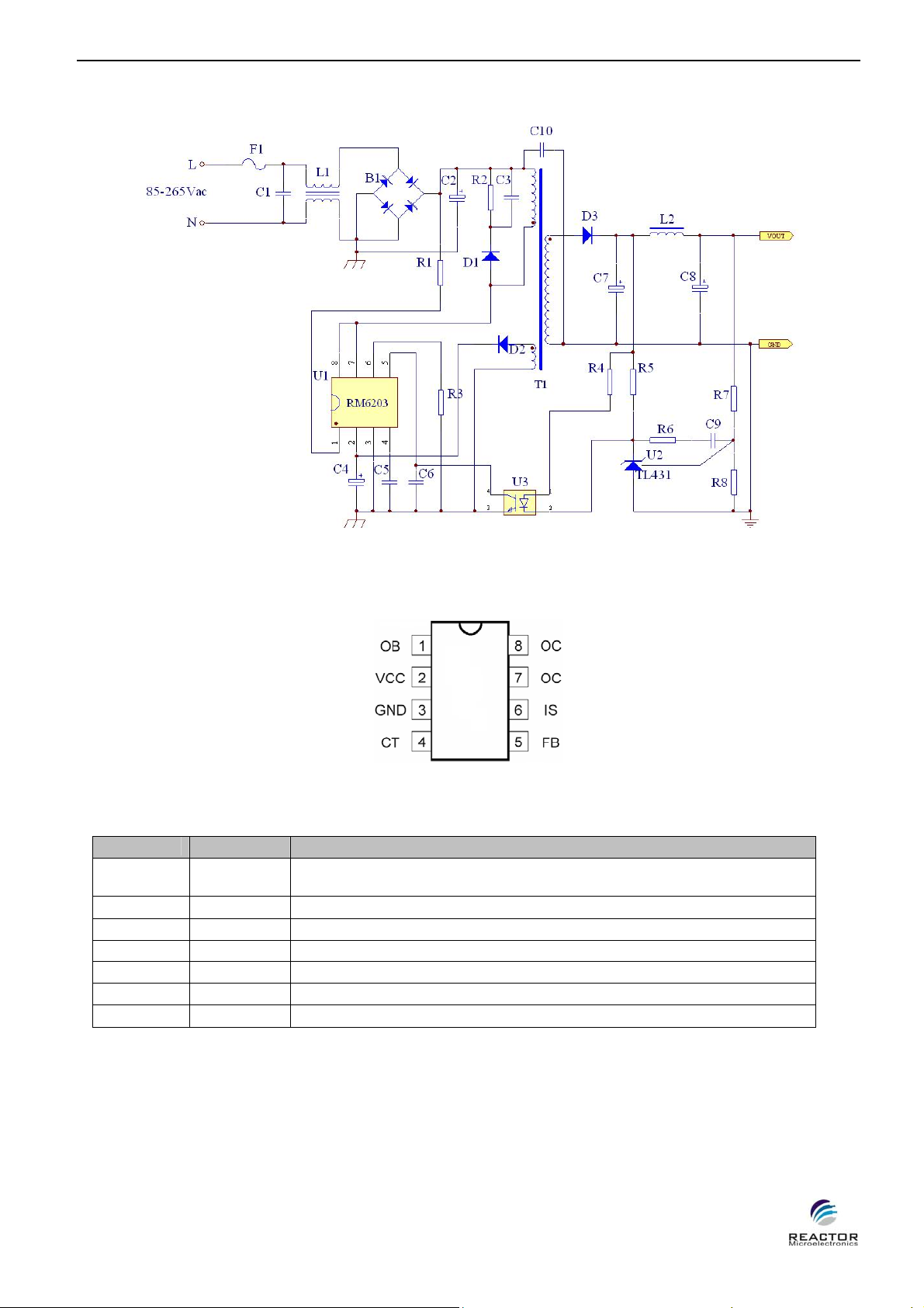
TYPICAL APPLICATION
PACKAGE INFORMATION
PIN FUNCTIONS
Pin Symbol Function Description
1 OB Base Pin of the Power Tube.(Enabling current input and connect to initiating
2 VCC Power Supply Pin
3 GND Ground Pin
4 CT Oscillation Capacitance Pin.(Connect to timing capacitance)
5 FB Feedback Pin
6 IS Current Inspection Pin
7、8
OC Output Pin( Connect to switching transformer)
TOP VIEW
DIP-8
resistance)
2 www.reactor-micro.com
Page 3
RM6203
ABSOLUTE MAXIMUM RATINGS(Note 1)
Supply Voltage VCC…………………………….… 18V Pin Input Voltage………………………………… VCC+0.3V
OC Voltage……………………………..…… -0.3-700V Switching Current………………….………………… 800mA
Total Dissipation Power………………..…… 1000mW Operating Temperature Range……..……………… 0-75℃
Storage Temperature Range…………… -40 - 150℃ Welding Temperature……......……………… +260℃,10S
ELECTRICAL CHARACTERISTICS
The specifications are applied at T=25℃, VCC=5.5-7.5V, Ct=680PF, RS=1Ω, unless otherwise noted.(Note 2)
Parameter Symbol Conditions Min Typ Max Units
Output Section
Max. Withstanding Voltage of
the Switching Tube
Saturation Voltage V
Output Rise Time TR CL=1nF 75 ns
Output Fall Time TF CL=1nF 75 ns
Output Limiting Current
Reference Section
Reference Output Voltage V
Line Regulation Vcc=5.5-9V 2 20 mV
Load Regulation Io=0.1-1.2mA 3 %
Temperature Stability 0.2
Output Noise Voltage F=10Hz-10KHz 50 uV
Long Term Stability
Oscillator Section
Oscillating Frequency F
Voltage Stability Vcc=5.5-9V 1 %
Temperature Stability
Oscillator Amplitude (Vp - p) 2.2 V
Feedback Section
Pull-up
Impedance
Current
Pull-Down
Resistor
Power Supply Suppression
Ratio
Current Sampling Section
Current Sampling Threshold V
Anti-Upper Limit Current IL 0.25 0.27 0.29 A
Power Supply Suppression
Ratio
PWM Section
Maximum Duty Ratio D
Minimum Duty Ratio D
Power Supply Current Section
Initiating Reception Current 1.6 2.4 3.2 mA
Initiating Static Current 55 80 uA
Static Current I
Start-up voltage 7.6 7.8 8.0 V
Oscillator Turn-off Voltage 4.2 4.4 4.6 V
I
SAT
REF
=10mA 700 V
OC
Ioc=250mA 1 V
Tj=0-100℃
250 270 290 mA
Io=1.0mA 2.4 2.5 2.6 V
mV/℃
1000 hours@85℃
Ct=680PF 59 66 73 KHz
OSC
Ta=0-85℃
FB=2.5V, IS=0V 0.55 0.6 0.65 mA Input
5 mV
1 %
30 KΩ
Vcc=5.5-9V 60 70 dB
CS
0.55 0.60 0.65 V
60 70 dB
MAX
MIN
Q
53 57 61 %
3.5 %
Vcc=8V 2.8 mA
www.reactor-micro.com 3
Page 4

RM6203
ELECTRICAL CHARACTERISTICS
The specifications are applied at T=25℃, VCC=5.5-7.5V, Ct=680PF, RS=1Ω, unless otherwise noted.(Note 2)(continued)
Re-enabling voltage 3.8 V
Over-Voltage Limiting
Threshold
Note1: Stresses beyond those listed under Absolute Maximum
Ratings may cause permanent damage to the device.
Exposure to any Absolute Maximum Rating condition for
extended periods may affect device reliability and lifetime.
9.5 10 10.5 V
Note2: TheRM6203 is guaranteed to meet performance
specifications from 0℃ to 70℃. Specifications over the -40℃
to 85℃ operating temperature range are assured by design,
characterization and correlation with statistical process
controls.
BLOCK DIAGRAM
OPERATION (Refer to Block Diagram)
In the enabling stage, when power is on, VR is closed; the
pull-up current source FB is closed; OE inputs enabling current
from power tube to VCC; OB controls the base current of the
power tube, limits the collector current of the power tube (i.e.
RM6203 initiates the reception current), so as to ensure the
safety of the power tube; when VCC voltage raises up to 7.8 V,
the enabling stage ends and it goes into the normal stage.
In the normal stage, VCC voltage should be maintained at
4.8V to 9.0V, VR outputs 2.5V reference; FB pull-up current
source is opened; the oscillator output OSC1 decides the
maximum duty ratio, output OSC2 tries to trigger the power
into open period, and the screened power tube turns on the
current peak; if FB is below 1.8V (approximately between 1.2V
and 1.8V), the oscillator period will then be increased, the
smaller the FB is, the wider the oscillator period will be, until
the stop of the oscillator (this feature will lower the stand-by
power consumption of the switch power source); if the external
feedback intends to make VCC higher than 10V, the internal
circuit feedback to FB will stabilize VCC at 9.8V (with this
feature, the internal circuit rather than the external feedback
circuit will be used to stabilize the output voltage, but the
stabilizing accuracy may be low); in the open period, OB
supplies base current to power tube, OE pulls down the emitter
of the power tube to IS, and the OB uses the slope current
driving (i.e. the OB open current is the function of IS, when IS
= 0V, OB open current is approximately 40mA, then the OB
4 www.reactor-micro.com
Page 5

open current will increase along with IS linearly, when IS raises
to 0.6V, the OB open current is approximately 100mA, this
feature will effectively utilize the output current of OB and lower
the power consumption of RM6203), if IS detects the specified
current of FB, it goes into close period; in the close period, OB
pulls down, the power tube may not be turned off immediately,
but OE clamps on 2.0V (after the power tube turns off, the
base will be reverse bias and the voltage withstanding
capacity is increased); in the open or close period, if it detects
the current exceeding upper limit of the power tube, then the
upper limit flip-flop will be put at the preferential position,
forcing FB to decrease and the duty ratio will turn smaller, so
that the power tube and transformer will be protected; at the
Normal Stage Switching Cycle Oscillogram
RM6203
beginning of next close period edge or if FB is below 1.8V, the
upper limit flip-flop will reset. Besides, the built-in heat
protection of RM6203 will widen the oscillator period when the
internal temperature is above 125 ℃ to ensure the
temperature of RM6203 will not exceed 135℃; the built-in
slope compensation will stabilize the open/close period when
RM6203 is at high duty ratio or in continuous current mode.
When VCC lowers to about 4.4V, the oscillator will be
closed, OSC1 and OSC2 will be at low level, and the power
source will be maintained at close period; when VCC goes on
lowering to about 3.8V, RM6203 will enter the enabling stage
again.
Global Oscillogram
www.reactor-micro.com 5
Page 6

RM6203
TEST DATA
V
IN
(VAC)
90Vac
100Vac
240Vac
256Vac
RM6203(12V)
P
V
IN
(W)
0.1 12.1
OUT
(V)
I
OUT
(A)
V
CC
(V)
V
(mVp
OR
P
OUT
p)
(W)
-
0 5.36 0
η
(%)
3.2 12.1 0.2 6.64 2.4 75.0
7.6 12.1 0.5 6.64 6.1 80.3
12.0 12.1 0.8 6.64 9.7 80.8
15.1 12.1
0.1 12.1
1.0 6.64 12.1 80.1
0 5.28 0
3.1 12.1 0.2 6.70 2.4 77.4
7.5 12.1 0.5 6.70 6.1 81.3
11.9 12.1 0.8 6.70 9.7 81.5
14.9 12.1
0.1 12.1
1.0 6.70 12.1 81.2
0 4.96 0
3.0 12.1 0.2 6.96 2.4 80.0
7.3 12.1 0.5 6.96 6.1 83.5
11.5 12.1 0.8 6.96 9.7 84.3
14.4 12.1
0.1 12.1
1.0 6.96 12.1 84.0
0 4.88 0
3.0 12.1 0.2 7.04 2.4 80.0
7.4 12.1 0.5 7.04 6.1 82.4
11.6 12.1 0.8 7.04 9.7 83.6
14.5 12.1
1.0 7.04 12.1 83.4
(A)
OPP
(A)
OCP
1.07 1.36
1.13 1.45
1.69 2.13
1.72 2.17
Average
η(%)
79.05
80.35
82.95
82.35
CEC
Standerd
η(%)
6 www.reactor-micro.com
Page 7

PACKAGE INFORMATION
DIP-8
RM6203
Dimensions
Millimeter Inch Symbol
Min. Typ. Max. Min. Typ. Max.
A 5.334 0.210
A1 0.381 0.015
A2 3.175 3.302 3.429 0.125 0.130 0.135
b 1.524 0.060
b1 0.457 0.018
D 9.017 9.271 10.160 0.355 0.365 0.400
E 7.620 0.300
E1 6.223 6.350 6.477 0.245 0.250 0.255
E 2.540 0.100
L 2.921 3.302 3.810 0.115 0.130 0.150
eB 8.509 9.017 9.525 0.335 0.355 0.375
θ° 0° 7° 15° 0° 7° 15°
www.reactor-micro.com 7
Page 8

 Loading...