

Page 1

RM5261A™ Microprocessor with 64-Bit System Bus Data Sheet
RM5261A™
Preliminary
RM5261A™ Microprocessor with 64-Bit
System Bus
Data Sheet
Proprietary and Confidential
Preliminary
Issue 2, September 2001
Proprietary and Confidential to PMC-Sierra, Inc and for its Customer’s Internal Use
Document ID: PMC-2002240, Issue 2
Page 2

RM5261A™ Microprocessor with 64-Bit System Bus Data Sheet
Preliminary
Legal Information
Copyright
© 2001 PMC-Sierra, Inc.
The information is proprietary and confidential to PMC-Sierra, Inc., and for its customers’ internal use. In
any event, you cannot reproduce any part of this document, in any form, without the express written
consent of PMC-Sierra, Inc.
PMC-2002240 (P2)
Disclaimer
None of the information contained in this document constitutes an express or implied warranty by PMCSierra, Inc. as to the sufficiency, fitness or suitability for a particular purpose of any such information or the
fitness, or suitability for a particular purpose, merchantability, performance, compatibility with other parts
or systems, of an y of t he pr oducts of PMC-Si erra , Inc., or an y port io n ther eof, r efer red to i n this document .
PMC-Sierra, Inc. expressly disclaims all representations and warranties of any ki nd regarding the contents
or use of the information, including, but not limited to, express and implied warranties of accuracy,
completeness, merchantability, fitness for a particular use, or non-infringement.
In no event will PMC-Sierra, Inc. be liable for any direct, indirect, special, incidental or consequential
damages, including, but not limited to, lost profits, lost business or lost data resulting from any use of or
reliance upon the infor ma tion, whether or not PMC-Sierra, Inc . has been advised of the possib il it y of s uch
damage.
Trademarks
RM5261A is a trademark of PMC-Sierra, Inc.
Contacting PMC-Sierra
PMC-Sierra, Inc.
105-8555 Baxter Place Burnaby, BC
Canada V5A 4V7
Tel: (604) 415-6000
Fax: (604) 415-6200
Document Information: document@pmc-sierra.com
Corporate Information: info@pmc-sierra.com
Technical Support: apps@pmc-sierra.com
Web Site: http://www.pmc-sierra.com
Proprietary and Confidential to PMC-Sierra, Inc and for its Customer’s Internal Use 2
Document ID: PMC-2002240, Issue 2
Page 3
RM5261A™ Microprocessor with 64-Bit System Bus Data Sheet
Preliminary
Revision History
Issue
No. Issue Date Details of Change
2 September 2001 Added 1.8 V to the feature: 1.65 V or 1.8 V core with 3.3 V or 2.5 V I/O (p9).
Changed recommended operating conditions VccInt to 1.57 V to 1.85 V and
VccP to 1.57 V to 1.85 V. Added VssP commercial and industrial values.
Modified Note 4.
Added reference to VccInt to Power Consumption table. Changed standby
modes to 350. Changed maximum worst case instruction mix to 1250. Modified
Note 1.
Modified SysClock Frequency and SysClock Period values in the Clock
Parameters table.
1 March 2001 Applied PMC-Sierra template to existing MPD (QED) FrameMaker document.
Revised features list, Absolute Maximum Ratings table, Recommended
Operating Conditions table, DC Electrical Characteristics table, Power
Consumption table, Clock Parameters table and the System Interface
Parameters table.
Proprietary and Confidential to PMC-Sierra, Inc and for its Customer’s Internal Use 3
Document ID: PMC-2002240, Issue 2
Page 4

RM5261A™ Microprocessor with 64-Bit System Bus Data Sheet
Preliminary
Document Conventions
The following conventions are used in this datasheet:
• All signal, pin, and bus names described in the text, such as ExtRqst*, are in boldface
typeface.
• All bit and field names describe d in the text , such as Interrupt Mask, are in an italic -bold
typeface.
• All instruction names, such as MFHI, are in san serif typeface.
Proprietary and Confidential to PMC-Sierra, Inc and for its Customer’s Internal Use 4
Document ID: PMC-2002240, Issue 2
Page 5

RM5261A™ Microprocessor with 64-Bit System Bus Data Sheet
Preliminary
Table of Contents
Legal Information ...........................................................................................................................2
Revision History .............................................................................................................................3
Document Conventions .................................................................................................................4
Table of Contents ..........................................................................................................................5
List of Figures ................................. ...... ....... ...................................... ....... ...... ....... ...... ..................7
List of Tables................................................................... ...... ....... ...... ....... ...... ....... ...... . ...... ...... .... 8
1 Features.................................................................................................................................. 9
2 Block Diagram .......................... ...... ....... ...... ....... ...... ....................................... ...... ....... .........10
3 Hardware Overview ...............................................................................................................11
3.1 Superscalar Dispatch ...................................................................................................11
3.2 CPU Registers .............................................................................................................11
3.3 Integer Unit ..................................................................................................................11
3.4 Pipeline ........................................................................................................................12
3.5 Register File .................................................................................................................12
3.6 ALU ..............................................................................................................................12
3.7 Integer Multiply/Divide ..................................................................................................12
3.8 Floating-Point Co-Processor ........................................................................................13
3.9 Floating-Point Unit .......................................................................................................13
3.10 Floating-Point General Register File ............................................................................15
3.11 System Control Co-processor (CP0) ............................................................................16
3.12 System Control Co-Processor Registers .....................................................................16
3.13 Virtual to Physical Address Mapping ............................................................................17
3.14 Joint TLB ......................................................................................................................18
3.15 Instruction TLB .............................................................................................................18
3.16 Data TLB ......................................................................................................................19
3.17 Cache Memory .............................................................................................................19
3.18 Instruction Cache .........................................................................................................19
3.19 Data Cache ..................................................................................................................19
3.20 Write buffer ..................................................................................................................21
3.21 System Interface ............. ...................................... ....... ...... ....... ...... ....... ......................21
3.22 System Address/Data Bus .... ....................................... ...... ....... ...... ....... ......................22
3.23 System Command Bus ................................................ ...... ....... ...... .............................22
3.24 Handshake Signals ......................................................................................................22
3.25 Non-overlapping System Interface ...............................................................................23
3.26 Enhanced Write Modes ................................................................................................24
3.27 External Requests ........................................................................................................24
3.28 Interrupt Handling ........................................................................................................25
3.29 Standby Mode .... ...... ....... ...................................... ....... ...... ....... ...... .............................25
3.30 JTAG Interface .............................................................................................................25
Proprietary and Confidential to PMC-Sierra, Inc and for its Customer’s Internal Use 5
Document ID: PMC-202240, Issue 2
Page 6

RM5261A™ Microprocessor with 64-Bit System Bus Data Sheet
Preliminary
3.31 Boot-Time Options .......................................................................................................25
3.32 Boot-Time Modes .........................................................................................................26
4 Pin Descriptions ....................................................................................................................27
5 Absolute Maximum Ratings ..................................................................................................30
6 Recommended Operating Conditions ...................................................................................31
7 DC Electrical Characteristics .................................................................................................32
8 Power Consumption ..............................................................................................................33
9 AC Electrical Characteristics .................................... ...... ....... ...... ....................................... .. .34
9.1 Capacitive Load Deration .............................................................................................34
9.2 Clock Parameters ........................................................................................................34
9.3 System Interface Parameters ............. ....... ...... ...... ....... ....................................... ...... ...35
9.4 Boot-Time Interface Parameters ..................................................................................35
10 Timing Diagrams ...................................................................................................................36
10.1 System Interface Timing ....................................... ....... ...... ....... ...... ....... ...... ....... ...... ...36
11 Packaging Information ..........................................................................................................37
12 RM5261A 208 QFP Package Numerical Pinout ...................................................................38
13 RM5261A 208 QFP Package Alphabetical Pinout ................................................................40
14 Ordering Information .............................................................................................................42
Proprietary and Confidential to PMC-Sierra, Inc and for its Customer’s Internal Use 6
Document ID: PMC-202240, Issue 2
Page 7

RM5261A™ Microprocessor with 64-Bit System Bus Data Sheet
Preliminary
List of Figures
Figure 1 Block Diagram .............................................................................................................10
Figure 2 CPU Registers .............................................................................................................11
Figure 3 Pipeline ........................................................................................................................12
Figure 4 CP0 Registers .............................................................................................................16
Figure 5 Kernel Mode Virtual Addressing (32-bit) .....................................................................17
Figure 6 Typical Embedded System Block Diagram ................................................................22
Figure 7 Processor Block Read .................................................................................................23
Figure 8 Processor Block Write .................................................................................................24
Figure 9 Clock Timing ................................................................................................................36
Figure 10 Input Timing ...............................................................................................................36
Figure 11 Output Timing ............................................................................................................36
Proprietary and Confidential to PMC-Sierra, Inc and for its Customer’s Internal Use 7
Document ID: PMC-2002240, Issue 2
Page 8

RM5261A™ Microprocessor with 64-Bit System Bus Data Sheet
Preliminary
List of Tables
Table 1 Integer Multiply/Divide Operations ................................................................................13
Table 2 Floating-Point Instruction Cycles ..................................................................................15
Table 3 Cache Attributes ...........................................................................................................21
Table 4 Boot-Time Mode Bit Stream .........................................................................................26
Table 5 System Interface ...........................................................................................................27
Table 6 Clock/Control Interface .................................................................................................28
Table 7 Interrupt Interface .........................................................................................................28
Table 8 JTAG Interface .............................................................................................................28
Table 9 Initialization Interface ....................................................................................................29
Table 10 Power Supply .............................................................................................................29
Proprietary and Confidential to PMC-Sierra, Inc and for its Customer’s Internal Use 8
Document ID: PMC-2002240, Issue 2
Page 9

1 Features
• Dual Issue superscalar microprocessor
• 250, 300, and 350 MHz operating frequencies
• Up to 420 Dhrystone 2.1 MIPS
• High-performance system interface
• 64-bit multiplexed system address/data bus for optimum price/performance
• High-performance write protocols maximize uncached write bandwidth
• Processor clock multipliers 2, 2.5, 3, 3.5, 4, 4.5, 5, 6, 7, 8, 9
• IEEE 1149.1 JTAG boundary scan
• Integrated on-chip caches
• 32 KB instruction and 32 KB data — 2 way set associative
• Per set locking
• Virtually indexed, physically tagged
• Write-back and write-through on a per page basis
• Pipeline restart on first doubleword for data cache misses
• Integrated memory management unit
• Fully associative joint TLB (shared by I and D translations)
• 48 dual entries map 96 pages
• Variable page size (4 KB to 16 MB in 4x increments)
RM5261A™ Microprocessor with 64-Bit System Bus Data Sheet
Preliminary
• High-performance floating-point unit: up to 700 MFLOPS
• Single cycle repeat rate for commo n single -prec ision ope rati ons and some double-p recision operations
• Two cycle repeat rate for double-precision multiply and double precision combined
multiply-add operations
• Single cycle repeat rate for single-precision combined multiply-add operation
• MIPS IV instruction set
• Floating point multiply-add instruction increases performance in signal processing
and graphics applications
• Conditional moves to reduce branch frequency
• Index address modes (register + register)
• Embedded application enhancements
• Specialized DSP integer Multiply-Accumulate instructions and 3-operand multiply
instruction
• I and D cache locking by set
• Optional dedicated exception vector for interrupts
• Fully static 0.18 micron CMOS design with power down logic
• Standby reduced power mode with WAIT instruction
• 1.65 V or 1.8 V core with 3.3 V or 2.5 V I/O
• 208-pin QFP package
Proprietary and Confidential to PMC-Sierra, Inc and for its Customer’s Internal Use 9
Document ID: PMC-2002240, Issue 2
Page 10
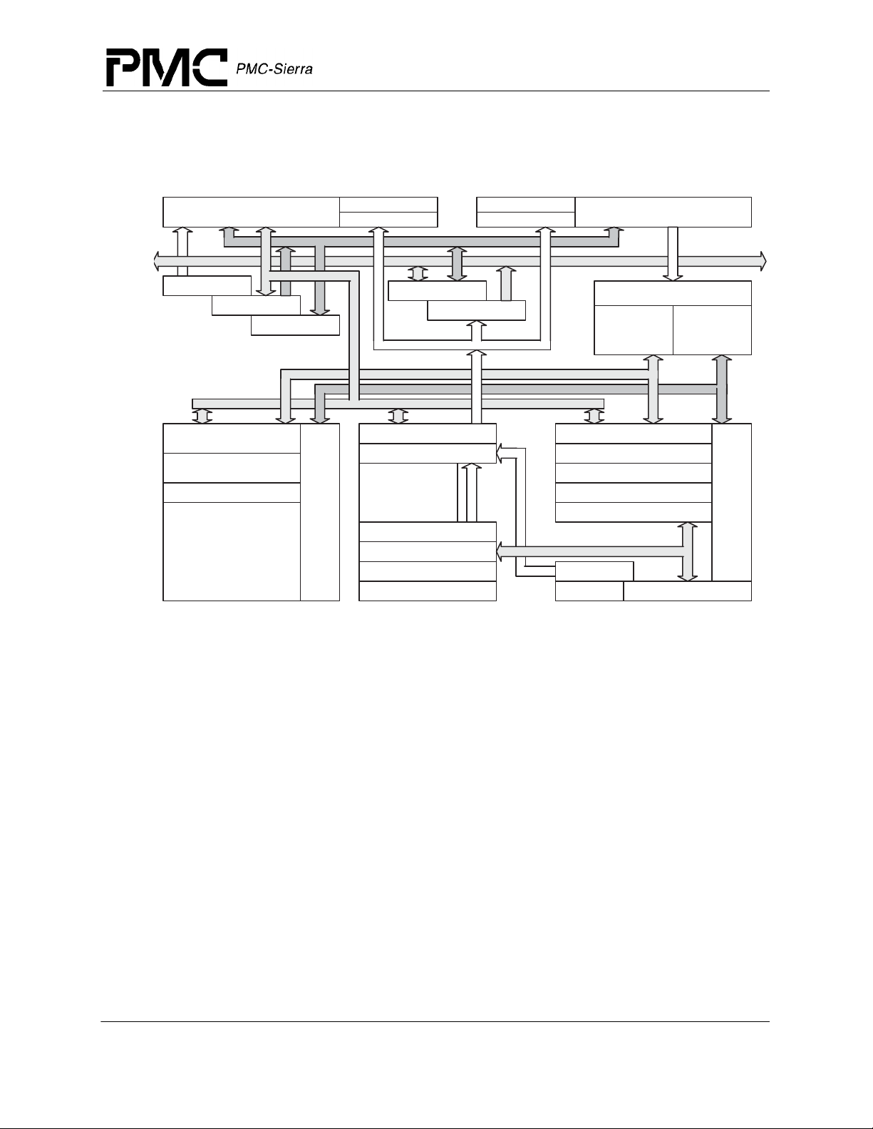
2 Block Diagram
Figure 1 Block Diagram
Primary Data Cache
2-way Set Associative
RM5261A™ Microprocessor with 64-Bit System Bus Data Sheet
Preliminary
DTag
DTLB
ITag
ITLB
Primary Instruction Cache
2-way Set Associative
A/D Bus
Pad Bus
Store Buffer
Write Buffer
D Bus
Floating-Point
Load/Align
Floating-Point
Register File
Packer/Unpacker
Floating-Point
MultAdd, Add, Sub,
Cvt, Div, Sqrt
Read Buffer
Coprocessor 0
System/Memory
Control
PC Incrementer
Floating-Point Control
Branch PC Adder
ITLB Virtual
Program Counter Int Mult, Div, Madd
Pad Buffer
Joint TLB
Address Buffer
IVA
DVA
FP Bus
FA Bus
Instruction Dispatch Unit
FP
Instruction
Register
Load Aligner
Integer Register File
Integer Address/Adder
Shifter/Store Aligner
Logic Unit
DTLB Virtual
PLL/Clocks
Integer
Instruction
Register
Integer Bus
Integer Control
Proprietary and Confidential to PMC-Sierra, Inc and for its Customer’s Internal Use 10
Document ID: PMC-2002240, Issue 2
Page 11
3 Hardware Overview
The RM5261A offers a high-level of integration targeted at high-performance embedded
applications. The key elements of the RM5261A are briefly described below.
3.1 Superscalar Dispatch
The RM5261A has an asymmetric superscalar dispatch unit which allows it to issue an integer
instruction and a floating-point computation instruction simultaneously. Integer instructions
include alu, branch, load/store, and floating-point load/store, while floating-point computation
instructions include fl oat in g-point add, subtract, combined multipl y- add, and convert. In
combination with its high- throug hput fully pipel ined fl oatin g-p oint exe cutio n unit, the supersc alar
capability of the RM5261A provides unparalleled price/perf ormance in computationally intensive
embedded applications.
3.2 CPU Registers
The RM5261A CPU contains 32 general purpose registers, two special purpose registers for
integer multiplicati on and division, a program counter, and no condition code bits. Figure 2 shows
the user visible state.
RM5261A™ Microprocessor with 64-Bit System Bus Data Sheet
Preliminary
Figure 2 CPU Registers
General Purpose Registers
63 0
0 63 0
r1 HI
r2 63 0
•LO
•
•
• 63 0
r29 PC
r30
r31
3.3 Integer Unit
The RM5261A implements t he MIPS IV I nstruct ion Set Ar chitect ure and i s there fore full y upward
compatible with applic ations that run on proce ssors implementing the earlier generation MIPS IIII instruction set s. Add it ion al ly, the RM5261A includes two implementat ion specific instruct io ns
not found in the baseline MIPS IV ISA but that are useful in the embedded market place. These
instructio ns are integer multiply-accumulat e (
Multiply/Divide Registers
Program Counter
MAD) and 3-operand integer multiply (MUL).
The RM5261A integer unit includes thirty-two general purpose 64-bit registers, a load/store
architecture with single cycle ALU operations (add, sub, logical, shift) and an autonomous
multiply/divide unit. Additional register resources include: the HI/LO resul t registers for the twooperand integer multiply/divide operations, and the program counter (PC).
Proprietary and Confidential to PMC-Sierra, Inc and for its Customer’s Internal Use 11
Document ID: PMC-2002240, Issue 2
Page 12
3.4 Pipeline
For integer operations, loads, stores, and other non-floating-point operations, the RM5261A
implements a 5-stage integer pipeline. In addi tion to the integer pipeline, the RM5261A
implements an extended 7-stage pipeline for floating-point operations.
RM5261A™ Microprocessor with 64-Bit System Bus Data Sheet
Preliminary
The RM5261A multiplies th e input
pipeline clock.
Figure 3 shows the RM5261A integer pipeline. As illustrated in the figure, up to five integer
instructions can be executing simultaneously.
Figure 3 Pipeline
I0
I1
I2
I3
I4
1I-1R:
2I:
2R:
1A:
1A:
1A-2A:
2A:
2A-2D:
1D:
2W:
2I1I 1R 2R 1A 2A 1D 2D 1W 2W
Instruction cache access
Instruction virtual to physical address translation
Register file read, Bypass calculation, Instruction decode, Branch address calculation
Issue or slip decision, Branch decision
Data virtual address calculation
Integer add, logical, shift
Store Align
Data cache access and load align
Data virtual to physical address translation
Register file write
3.5 Register File
SysClock by 2, 2.5, 3, 3.5, 4, 4.5, 5, 6, 7, 8, or 9 to prod uce the
2I1I 1R 2R 1A 2A 1D 2D 1W 2W
2I1I 1R 2R 1A 2A 1D 2D 1W 2W
2I1I 1R 2R 1A 2A 1D 2D 1W 2W
2I1I 1R 2R 1A 2A 1D 2D 1W 2W
one cycle
The RM5261A has thirty-two general purpose registers with register location 0 (r0) hard-wired to
a zero value. These registers are used for scalar integer operations and address calculation. The
register file has two read ports and one write port and is fully bypassed to minimize operation
latency in the pipeline.
3.6 ALU
The RM5261A ALU consists of an integer adder/subtractor, a logic unit, and a shifter. The adder
performs address calculations in addition to arithmetic operations. The logic unit performs all
logical and zero s hift d ata moves . The shift er per forms s hifts and store align ment o perat ions. Eac h
of these units is optimized to perfor m all operations in a sing l e processor cycle.
3.7 Integer Multiply/Divide
The RM5261A has a dedicated i ntege r multi ply/di vide un it opt imized f or hig h-spee d multip ly a nd
multiply-accumulate operations. Table 1 shows the performance of the multiply/divide unit on
each operation.
Proprietary and Confidential to PMC-Sierra, Inc and for its Customer’s Internal Use 12
Document ID: PMC-2002240, Issue 2
Page 13
RM5261A™ Microprocessor with 64-Bit System Bus Data Sheet
Preliminary
Table 1 Integer Multiply/Divide Operations
Operand
Opcode
MULT/U, MAD/U
MUL 16 bit 3 2 1
DMULT, DMUL TU
DIV, DIVD any 36 36 0 DDIV,
DDIVU
Size Latency
16 bit 3 2 0 32 bit 4 3 0
32 bit 4 3 2 any 7 6 0
any 68 68 0
Repeat
Rate
Stall
Cycles
The baseline MIPS IV ISA specifies that the results of a multiply or divide operation be placed in
the Hi and Lo registers. These values can then be transferred to the general purpose register file
using the Move-from-Hi and Move-from-Lo (
MFHI/MFLO) instructi ons.
In addition to the baseline MIPS IV integer multiply instructions, the RM5261A also implements
the 3-operand multiply instruction,
MUL. This instruction specifies that the multiply result go
directly to the integer register file rather than the Lo register. The portion of the multiply that
would have normally gone i nto the Hi re gister i s discard ed. For applicat ions where i t is known tha t
the upper half of the multiply result is not required, using the
necessity of executing an explicit
MFLO instruction.
MUL instruction eliminates the
The multiply-add instructions,
MAD and MADU, multiply two ope rands and add the resulting
product to the current contents of the Hi and Lo registers. The multip ly-accumulate operat ion is
the core primitive of almost all signal processing algorithms, allowing the RM5261A to eliminate
the need for a separate DSP engine in many embedded applications.
3.8 Floating-Point Co-Processor
The RM5261A incorporate s a hig h-p erfor mance fu lly pi pe lined float ing-p oint c o-proc ess or whic h
includes a floating-po int register file and autonomous execution units for multiply/a dd/convert and
divide/square root. The floating-point coprocessor is a tightly coupled execution unit, decoding
and executing instructions in parallel with, and in the case of floating-point loads and stores, in
cooperation with the integer unit. The superscalar capabilities of the RM5261A allow floatingpoint computation instructions to issue concurrently with integer instructions.
3.9 Floating-Point Unit
The RM5261A floating-point execution unit supports single and double precision arithmetic, as
specified in the IEEE S tanda rd 754. The ex ecution uni t is broken i nto a separa te divide /square ro ot
unit and a pipelined multiply/add unit. Overlap of the divide/square root and multiply/add
operations is supported.
The RM5261A maintains fully precise floating-point exceptions while allowing both overlapped
and pipelined operations. Precise exceptions are extremely important in object-oriented
programming environments and highly desirable for debugging in any environment.
Proprietary and Confidential to PMC-Sierra, Inc and for its Customer’s Internal Use 13
Document ID: PMC-2002240, Issue 2
Page 14

RM5261A™ Microprocessor with 64-Bit System Bus Data Sheet
Floating-point operations include:
•add
• subtract
• multiply
• divide
• square root
• reciprocal
• reciprocal square root
• conditional moves
• conversion between fixed-point and floating-point format
• conversion between floating-point formats
• floating-point compare
Table 2 gives the latencies of the floating-point instructions in internal processor cycles.
Preliminary
Proprietary and Confidential to PMC-Sierra, Inc and for its Customer’s Internal Use 14
Document ID: PMC-2002240, Issue 2
Page 15

RM5261A™ Microprocessor with 64-Bit System Bus Data Sheet
Table 2 Floating-Point Instruction Cycles
Operation Latency Repeat Rate
fadd 4 1 fsub 4 1 fmult 4/5 1/2 fmadd 4/5 1/2 fmsub 4/5 1/2 fdiv 21/36 19/34 fsqrt 21/36 19/34 frecip 21/36 19/34 frsqrt 38/68 36/66 fcvt.s.d 4 1 fcvt.s.w 6 3 fcvt.s.l 6 3 fcvt.d.s 4 1 fcvt.d.w 4 1 fcvt.d.l 4 1 fcvt.w.s 4 1 fcvt.w.d 4 1 fcvt.l.s 4 1 fcvt.l.d 4 1 fcmp 1 1 fmov 1 1 fmovc 1 1 fabs 1 1 fneg 1 1
Note
1. Numbers are represented as single/double precision format.
Preliminary
3.10 Floating-Point General Register File
The floating-point general register file (FGR) is made up of thirty-two 64-bit registers. Wi th the
floating-point load and store double instructions (
take advantage of the 64-bit wide data cache and issue a floating-point coprocessor load or store
doubleword instruction in every cycle.
The floating-point c ont rol register space contains two register s; one for determining conf iguration
and revision in format ion fo r the c oproces sor, and one for control and statu s inf ormati on. Thes e are
primarily used for diagnos ti c sof twa re, exception handling, st at e sav ing and res tor ing, and control
of rounding modes. To support superscalar operation, the FGR has four read ports and two write
ports, and is fully bypassed to minimize operation latency in the pipeline. Three of the read ports
and one write port are used t o support the combi ned multi ply -add ins truct ion whil e the fo urth re ad
and second write port allows a concurrent floating-point load or store.
Proprietary and Confidential to PMC-Sierra, Inc and for its Customer’s Internal Use 15
Document ID: PMC-2002240, Issue 2
LDC1 and SDC1) the floating-point unit can
Page 16

RM5261A™ Microprocessor with 64-Bit System Bus Data Sheet
3.11 System Control Co-processor (CP0)
The system control coprocessor, also called coprocessor 0 or CP0 in the MIPS architecture, is
responsible for the virtual memory sub-system, the exception control system, and the diagnostics
capability of the processor. In the MIPS architecture, the system control co-processor (and thus the
kernel software) is implementati on dependent.
The memory management unit co ntrol s the virtu al memory syste m page mapping . It co nsist s of a n
instruction address translation buffer, ITLB, a data address translation buffer, DTLB, a Joint
instruction and data ad dress transl ation buf fer , JTLB, and co-pr ocessor re gisters used by the virtual
memory mapping sub-system.
3.12 System Control Co-Processor Registers
The RM5261A incorporates all system control co-processor (CP0) registers on-chip. These
registers provide the path through which the virtual memory system’s page mapping is examined
and modified, exceptions are handled, and operating modes are controlled (kernel vs. user mode,
interrupts enabled or disabled, cache features). In addition, the RM5261A includes registers to
implement a real-t ime cyc le coun ti ng faci lity to ai d in ca che dia gnosti c tes ting a nd to assi st in data
error detection.
Preliminary
Figure 4 shows the CP0 registers.
Figure 4 CP0 Registers
PageMask
5*
EntryHi
10*
47
(entries protected
from TLBW R)
TagLo
28*
* Register number
LLAddr
17*
0
EntryLo0
2*
EntryLo1
3*
TLB
TagHi
29*
Used for memory
management
Index
0*
Random
1*
Wired
6*
PRId
15*
Config
16*
Context
4*
Count
9*
Status
12*
EPC
14*
ECC
26*
BadVAddr
8*
Compare
11*
Cause
13*
XContext
20*
CacheErr
27*
ErrorEPC
30*
Used for exception
processing
Proprietary and Confidential to PMC-Sierra, Inc and for its Customer’s Internal Use 16
Document ID: PMC-2002240, Issue 2
Page 17

RM5261A™ Microprocessor with 64-Bit System Bus Data Sheet
3.13 Virtual to Physical Address Mappin g
The RM5261A provides three modes of virtual addressing:
• user mode
•kernel mode
• supervisor mode
This mechanism allows system so ftware to provide a sec ure enviro nment for user processes. Bits
in the CP0 register Status determine which virtual addressing mode is used. In the user mode, the
RM5261A provides a single, uniform virtual address space of 1 TB (2 GB in 32-bit mode).
When operating in the kernel mode, four distinct virtual address spaces, totalling over 2.5 TB (4
GB in 32-bit mode), are simultaneously available and are differentiated by the high-order bits of
the virtual address.
The RM5261A processors also support a supervisor mode in which the virtual address space over
2 TB (2.5 GB in 32-bi t mode), div ided i nto t hree regio ns based o n the high- order bits of t he vir tual
address.
Preliminary
When the RM5261A is configured as a 64-bit microprocessor, the virtual address space layout is
an upward compatible extension of the 32-bit virtual address space layout.
Figure 5 shows the address space layout for 32-bit operation
Figure 5 Kernel Mode Virtual Addressing (32-bit)
0xFFFFFFFF Kernel virtual address space
(kseg3)
0xE0000000 0xDFFFFFFF Supervisor virtual address space
0xC0000000 0xBFFFFFFF Uncached kernel physical addr ess space
0xA0000000 0x9FFFFFFF Cached kernel physical address space
0x80000000 0x7FFFFFFF User virtual address space
Mapped, 0.5GB
(ksseg)
Mapped, 0.5GB
(kseg1)
Unmapped, 0.5GB
(kseg0)
Unmapped, 0.5GB
(kuseg)
Mapped, 2.0GB
0x00000000
Proprietary and Confidential to PMC-Sierra, Inc and for its Customer’s Internal Use 17
Document ID: PMC-2002240, Issue 2
Page 18

3.14 Joint TLB
For fast virtual-to-physical address translation, the RM5261A uses a large, fully associative TLB
that maps 96 virtual pages t o their corre spondin g physic al a ddress es. As indi cated by its name, the
joint TLB (JTLB) is used for both instruction and data translations. The JTLB is organized as 48
pairs of even-odd entrie s, an d maps a virt ual addr ess and ad dress space ide nti fier int o th e lar ge, 64
GB physical address space.
Two mechanisms are provided to assist in controlling the amount of mapped space and the
replacement characte ristic s of various memory regi ons. First, the page si ze can be conf igured, on a
per-entry bas is , to use page sizes in the range of 4 KB to 16 MB (i n mul ti pl es of 4). The CP0 Page
Mask register is loaded with the desired page size of a mapping, and that size is stored into the
TLB along with the virtual address when a new entry is written. Thus, operating systems can
create spec ial purpose maps; for example, an entire frame buffer can be m emory mapped using
only one TLB entry.
The second mechanism controls the replacement algorithm when a TLB miss occurs. The
RM5261A provides a random replacement algorithm to select a TLB entry to be written with a
new mapping; however, the processor also provides a mechanism whereby a system specific
number of mappings can be locked into the TLB, thereby avoiding random replacement. This
mechanism uses the Wired register and allows the op erati ng sys tem to gu arant ee tha t cer tain pa ges
are always mapped for performance reasons and for deadlock avoidance. This mechanism also
facilitates the design of real-time s ystems by allowing deterministic access to critical software.
RM5261A™ Microprocessor with 64-Bit System Bus Data Sheet
Preliminary
The JTLB also contains information that controls the cache coherency protocol for each page.
Specifically, each page has attribute bits to determine whether the coherency algorithm is one of
the followin g:
• uncached
• non-coherent write-back
• non-coherent write-through with write-allocate
• non-coherent write-through without write-allocate
• sharable
• exclusive
•update
The non-coherent protocols are used for both code and data on the RM5261A, with data using
write-back or write-through depending on the application.
The coherency attributes generate coherent transaction types on the system interface. However, in
the RM5261A cache coherency is not supported. Hence the coherency attributes should never be
used.
3.15 Instruction TLB
The RM5261A implements a 2-entry instruction TLB (ITLB) to minimize contention for the
JTLB, eliminate the timing critical path of translating through a large associative array, and save
power. Each ITLB entry maps a 4 KB page. The ITLB improves performance by allowing
instruction address translation to occur in parallel with data address translation. When a miss
Proprietary and Confidential to PMC-Sierra, Inc and for its Customer’s Internal Use 18
Document ID: PMC-2002240, Issue 2
Page 19

occurs on an instruction address translation by the ITLB, the least-recently used ITLB entry is
filled from the JTLB. Th e operation of the ITLB is completely transparent to the user.
3.16 Data TLB
The RM5261A implements a 4-entry data TLB (DTLB) for the same reasons cited above for the
ITLB. Each DTLB entry maps a 4 KB page. The DTLB improves performance by allowing data
address translation to occur in par allel with instr uct ion address tran sl at ion . Wh en a miss occurs on
a data address translation by the DTLB, the DTLB is fil led from th e JTLB. The DTLB refill is
pseudo-LRU: the least recently used entry of the least recently used pair of entries is filled. The
operation of the DTLB is completely transparent to the user.
3.17 Cache Memory
The RM5261A incorporates on-chip instruction and data caches that can be accessed in a single
processor cycle. Each cache has its own 64-bit data path and both caches can be accessed
simultaneously. The cache subsystem provides the integer and floating-point units with an
aggregate bandwidth of 3.2 GB per second at an internal clock frequency of 200 MHz.
3.18 Instruction Cache
RM5261A™ Microprocessor with 64-Bit System Bus Data Sheet
Preliminary
The RM5261A incorporates a two-way set associative on-chip instruction cache. This virtually
indexed, physically tagged cache is 32 KB in size and is protected with word parity.
Since the cache is virtually indexed, the virtual-to-physical address translation occurs in parallel
with the cache access, further increasing performance by allowing these two operations to occur
simultaneously. The cache tag contains a 2 4-bit physic al ad dre ss, a valid bit, and a s ingle pari ty bit .
The instruction cache is 64-bits wide and can be accessed each processor cycle. Accessing 64 bits
per cycle allows the instruction cache to supply two instructions per cycle to the superscalar
dispatch unit. For typical code sequences where a floating-point load or store and a floating-point
computation instruction are being issued together in a loop, the entire bandwidth available from
the instruction cache is consumed.
Cache miss refill writes 64 bits per cycle to minimize the cache miss penalty. The line size is eight
instructions (3 2 bytes) to maximi ze the p erfor mance of c ommunic ation betwe en the p rocess or and
the memory system.
The RM5261A supports cac he loc king. The conte nts of set A of th e c ache ca n be locked by se ttin g
a bit in the coprocessor 0 Status register. Locking the set prevents its contents from being
overwritten by a subsequent cache miss. Refills occur only into set B. This mechanism allows the
programmer to lock critical code into the cache, thereby guaranteeing d eterministic behavior for
the locked code sequence.
3.19 Data Cache
For fast, single cycle data access, the RM5261A includes a 32 KB on-chip data cache that is twoway set ass ociative w ith a fixed 32 -byte (eight words) line size.
The data cache is protected with byte parity and its tag is protected with a single parity bit. It is
virtually indexed and physically tagged to allow simultaneous address translation and data cache
access.
Proprietary and Confidential to PMC-Sierra, Inc and for its Customer’s Internal Use 19
Document ID: PMC-2002240, Issue 2
Page 20

RM5261A™ Microprocessor with 64-Bit System Bus Data Sheet
Preliminary
Cache protocols supported for the data cache are:
1. Uncached Data loads and instr uction fetches from uncached memory space ar e b rou ght in from the main
memory to the register file and the execution unit, respectfully. The caches are not accessed.
Data store s to uncached memory space go directly to the main memory without updating the
data cache.
2. Write-back Loads and instruction fetches first search the cache, reading main memory only if the desired
data is not cache resident. On data store operations, the cache is first searched to determine if
the target address is cache resident. If it is resident, the cache contents are updated, and the
cache line is marked for later write-back. If the cache lookup misses, the target cache line is
first brought into the cache and then the write is performed as above.
3. Write-through with write allocate Loads and instruction fetches first search the cache, reading main memory only if the desired
data is not cache resident. On data store operations, the cache is first searched to determine if
the target address is cache resident. If it is resident, the cache contents are updated and main
memory is written, leaving the write-back bit of the cache lin e unchang ed. If t he cache lookup
misses, the target line is first brought into the cache and then the write is performed as above.
4. Write-through without write allocate Loads and instruction fetches first search the cache, reading main memory only if the desired
data is not cache resident. On data store operations, the cache is first searched to determine if
the target address is cache resident. If it is resident, the cache contents are updated and main
memory is written, leaving the write-back bit of the cache line unchang ed. If the ca che lookup
misses, then only main memory is writt en.
The most commonly used write policy is write-back, where a store to a cache line does not
immediately cause main memory to be updated. This increases system performance by reducing
bus traffic and eliminating the bottleneck of waiting for each store operation to finish before
issuing a subsequent memory operation. Software can, however, select write-through on a perpage basis when appropriate, such as for frame buffers.
Associated with the data cache is the store buffer. When the RM5261A executes a store
instruction, this single-entry buffer gets wr itten with the store data while the t ag comparison is
performed. If the tag matches, then the data is written into the data cache in the next cycle that the
data cache is not accessed (the next non-load cycle). The store buffer allows the RM5261A to
execute a store every processor cycle and to perform back-to-back stores without penalty. In the
event of a store immediately followed by a load to the same address, a combined merge and cache
write occurs such that no penalty is incurred. The RM5261A cache attributes for both the
instruction and data caches are summarized in Table 3.
Proprietary and Confidential to PMC-Sierra, Inc and for its Customer’s Internal Use 20
Document ID: PMC-2002240, Issue 2
Page 21

T a ble 3 Cache Attributes
Characteristics Instruction Data
Size 32KB 32KB Organization 2-way set associative 2-way set associativ e Line size 32B 32B Index vAddr
Tag pAddr Write policy n.a. write-back/write-through
Read order sub-block sub-block Write order sequential sequential miss restart after transfer of entire line first double Parity per-word per-byte Cache locking set A set A
3.20 Write buffer
RM5261A™ Microprocessor with 64-Bit System Bus Data Sheet
Preliminary
11..0
31..12
vAddr
pAddr
11..0
31..12
Writes to external memory, whether cache miss write-backs or st ores to uncach ed or write-t hrough
addresses, use the on-chip write buffer. The write buffer holds up to four 64-bit address and data
pairs. The entire buffer is used for a data cache write-back and allows the processor to proceed in
parallel with the memory update. For uncached and write-through stores, the write buffer
significantly increases performance by decoupling the
execution stream.
3.21 System Interface
The system interface consists of a 64-bit Address/Data bus with 8 parity check bits and a 9-bit
command bus. In addition, there are 6 handshake signals and 6 interrupt inputs. The interface is
capable of transfer ring data between the processor and memory at a p eak rate of 800MB/ sec with a
100MHz SysClock.
Figure 6 shows a typical embedded system using the RM5261A. In this example, a bank of
DRAMs and a memory controller ASIC share the processor’s
controller provides separate ports to a boot ROM and an I/O system.
SysAD bus transfers from the instruction
SysAD bus while the memory
Proprietary and Confidential to PMC-Sierra, Inc and for its Customer’s Internal Use 21
Document ID: PMC-2002240, Issue 2
Page 22

RM5261A™ Microprocessor with 64-Bit System Bus Data Sheet
Figure 6 T ypical Embedded System Block Diagram
Control
DRAM
Address
Flash/
Boot
Rom
Preliminary
72
Latch
RM5261A
72
23
3.22 System Address/Data Bus
The 64-bit System Address Data (SysAD) bus is used to transfer addresses and data between the
RM5261A and the rest of the sys tem. It is prote cted with an 8 -bit parit y check bus (SysADC). The
system int erface is configurable to allow easy interfacing to memory and I/O systems of varying
frequencies.
The Block Write data rate, Non-block Write protocol, and the Output Drive strength are
programmable at Boot time via the Mode Control bits. The rate at which the processor receives
data is also fully controlled by the external device.
3.23 System Command Bus
The RM5261A interface has a 9-bit System Command (SysCmd) bus. The command bus
indicates whether the SysAD bus carries address or data information on a per-clock basis. If the
SysAD carries address, the SysCmd bus indicates what type of transaction is to take place (for
example, a read or write). If the SysAD carries data, the SysCmd bus provides information about
the data (for example, this is the last data word transmitted, or the data contains an error). The
SysCmd bus is bidirectional to support both processor requests and external requests to the
RM5261A. Processor requests are initiated by the RM5261A and responded to by an external
device. External requests are issued by an external device and require the RM5261A to respond.
Memory I/O
Controller
8
x x
PCI Bus
The RM5261A supports one- to eight-byte transfers as well as block transfers on the SysAD bus.
In the case of a sub-double word transfer, the three low-order addr ess bits give the byte addres s of
the transfer, and the SysCmd bus indicates the number of bytes being transferred.
3.24 Handshake Signals
There are six handshake signals on t he system interface. Two of these, RdRdy* and WrRdy*, are
used by an external device to indicate to the RM5261A whether it can accept a new read or write
transaction. The RM5261A sampl es t hese signals before deasserting the ad dress on read and wri te
requests.
Proprietary and Confidential to PMC-Sierra, Inc and for its Customer’s Internal Use 22
Document ID: PMC-2002240, Issue 2
Page 23

RM5261A™ Microprocessor with 64-Bit System Bus Data Sheet
ExtRqst* and Release* are used to transfer control of the SysAD and SysCmd buses from the
processor to an external device. When an external device needs to control the interface, it asserts
ExtRqst*. The RM5261A responds by asserting Release* to release the system interfa ce to slave
state.
ValidOut* and ValidIn* are used by the RM5261A and the external device respectively to
indicate that there is a valid address, a command, or data on the SysAD and SysCmd buses. The
RM5261A asserts ValidOut* when it is driving these buses with a valid address, a command, or
data, and the extern al device d rives ValidIn* when it has control of the buse s and is dri ving a vali d
address, a command, or data.
3.25 Non-overlapping System Interface
The RM5261A implements a non-overlapping system interface, meaning that only one processor
request may be outstanding at a time and that the request must be serviced by an external device
before the RM5261A issues another request. The RM5261A can issue read and write requests to
an external device, whereas an external device can issue null and write requests to the RM5261A.
For processor reads the RM5261A asserts ValidOut* and simultaneously drives the address and
read command on the SysAD a nd SysCmd buses res pecti vely. If the system interface h as RdRdy*
asserted, then the processor tristates its drivers and releases the system interface to the slave state
by asserting Release*. The external device can then begin sending data to the RM5261A.
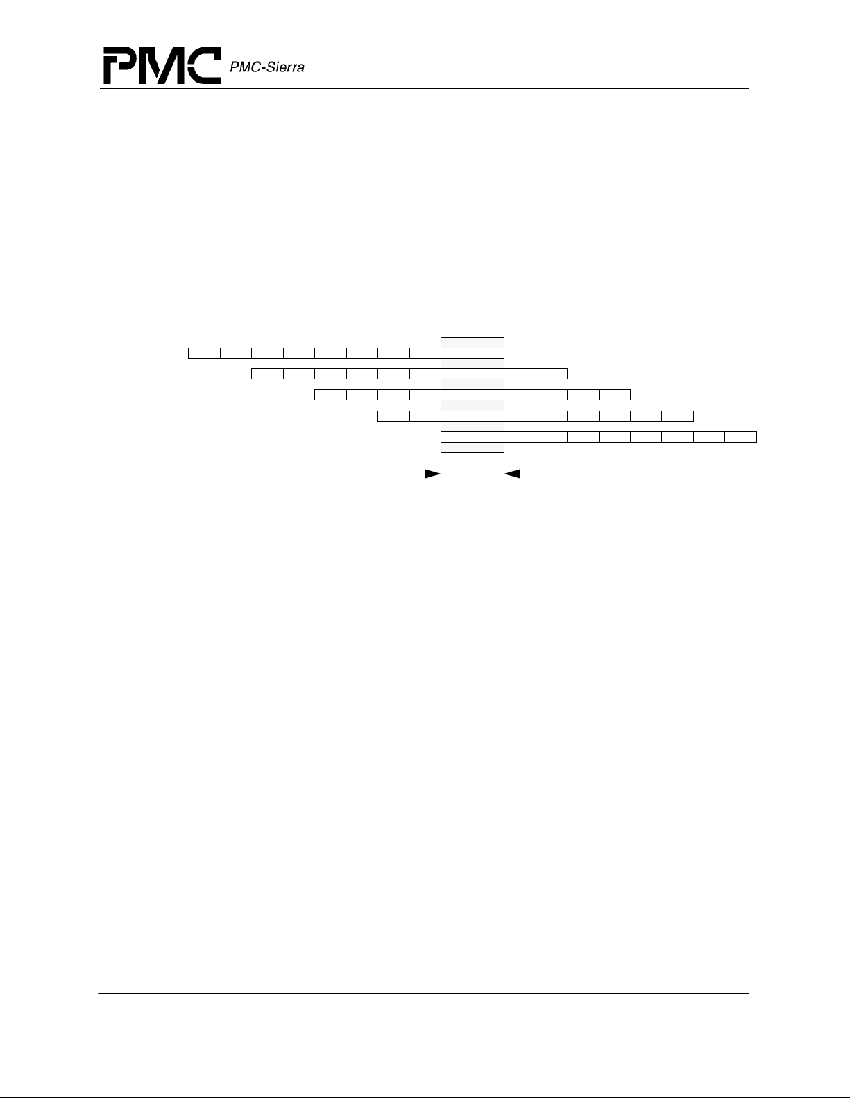
Preliminary
Figure 7 shows a processor block read request and the external agent read response. The read
latency is 4 cycles (ValidOut* to ValidIn*), and the response data pattern is DDDD, indicating
that data can be transferred on every clock with no wait states in-betwee
Figure 7 Processor Block Read
SysClock
SysAD
SysCmd
ValidOut*
ValidIn*
RdRdy*
WrRdy*
Release*
Addr
Read NData NData NData NEOD
Data0 Data1 Data2 Data3
n.
Figure 8 shows a process or bloc k writ e using write respons e patt ern DDDD, or code 0, o f the b oottime mode select options.
Proprietary and Confidential to PMC-Sierra, Inc and for its Customer’s Internal Use 23
Document ID: PMC-2002240, Issue 2
Page 24

Figure 8 Processor Block Write
SysClock
RM5261A™ Microprocessor with 64-Bit System Bus Data Sheet
Preliminary
SysAD
SysCmd
ValidOut*
ValidIn*
RdRdy*
WrRdy*
Release*
Addr Data0 Data1 Data2 Data3
Write NData NData NData NEOD
3.26 Enhanced Write Modes
The RM5261A implements two enhancements to the original R4000 write mechanism: Write
Reissue and Pipeline Writes. The original R4000 allowed a write address cycle on the SysAD bus
only once every four SysClock cycles. Hence for a non-block write, this meant that two out of
every four cycles were wait states.
Pipelined write mode eliminates these two wait states by allowing the processor to drive a new
write address onto the bus immediately after the previous write data cycle. This allows for higher
SysAD bus utilization. However, at high bus frequencies the processor may drive a subsequent
write onto the bus prior to the time the external agent deasserts WrRdy*, indicating that it can not
accept another write cycle. This can cause the write cycle to be missed.
Write re issue mode is an enhance ment to pipeli ned writ e mode and allo ws the proce ssor to re is sue
missed write cycles. If WrRdy* is deasserted during the issue phase of a write operation, the cycle
is aborted b y the processor and reissued at a later time.
In write reissue mode, a write rate of one write every two bus cycles can be achieved. Pipelined
writes have the same two bus cycle write repeat rate, but can issue one additional write following
the deasse rtion of WrRdy*.
3.27 External Requests
The External Request pin , ExtRqst*, is asserted by the e xternal agent when it requires mastershi p
of the system interface, either to perform an independent transfer or to write to the interrupt
register within the RM5261A. An independent transfer is a data transfer between two external
agents or be tween an external age nt and memory or periph eral on the system interface. Following
the asserting of the ExtRqst*, the RM5261A tri-states its drivers allowing the external agent to
use the system interface buses to complete an independent transfer. The external agent is
responsible for returning mastership of the sy stem interface to the RM5261A when it has
completed the independent transfer and does so by executing an External Null cycle.
Proprietary and Confidential to PMC-Sierra, Inc and for its Customer’s Internal Use 24
Document ID: PMC-2002240, Issue 2
Page 25

3.28 Interrupt Handling
The RM5261A supports a de di cat ed interrupt vector. When enabled by the r eal time executive (by
setting a bit in th e Cause regis ter), int errupts vector to a s pecific a ddress tha t is not sha red with any
of the other exce ption types . Thi s capa bility eli minate s the need to go through the no rmal so ft ware
routine for exception decode and dispatch, thereby lowering interrupt latency.
3.29 Standby Mode
The RM5261A provides a means to reduce the amount of power consumed by the internal core
when the CPU is not performing any useful operations. This state is known as Standby Mode.
RM5261A™ Microprocessor with 64-Bit System Bus Data Sheet
Preliminary
Executing the
Mode. If the SysAD bus is idle when the wait instruction completes the W pipe stage, the internal
processor clock stops and the pipeline is suspended. The phase lock loop, or PLL, internal timer/
counter, and the “wake up” input pins: Int[5:0]*, NMI*, ExtReq*, Reset*, and ColdReset*
continue to operate in their normal fashion. If the SysAD bus is not idle when the WAIT
instruction completes the W pipe-stage, then the
is completed. Once the processor is in Standby, any interrupt, including the internally generated
timer interrupt, causes the processor to exit Standby mode and resume operation where it left off.
The
WAIT instruction is typically inserted in the idle loop of the operating system or real time
executive.
WAIT instruction enables interrupts and causes the processor to enter Standby
3.30 JTAG Interface
The RM5261A interface supports JTAG Test Access Port (TAP) boundary scan in conformance
with the IEEE 1149.1 specification. The JTAG interface is especially helpful for checking the
integrity of the processors pin connections.
3.31 Boot-Time Options
Fundamental operational modes for the processor are initialized by the boot-time mode control
interface. This serial interface operates at a very low frequency (SysClock divided by 256). The
low frequency operation allows the initialization information to be kept in a low cost EPROM or
system interface ASIC.
Immediately after the VccOK signal is asserted, the processor reads a serial bit stream of 256 bits
to initialize all the fundamental operational modes. ModeClock runs continuously from the
assertion of VccOK.
WAIT is treated as a NOP until the bu s operation
Proprietary and Confidential to PMC-Sierra, Inc and for its Customer’s Internal Use 25
Document ID: PMC-2002240, Issue 2
Page 26

3.32 Boot-Time Modes
The boot-time serial mode stream is defined in Table 4. Bit 0 is the bit presented to the processor
as the first bit in the stream when VccOK is asserted. Bit 255 is the last bit transferred.
Table 4 Boot-Time Mode Bit Stream
Mode
bit Description
0 reserved (must be zero) 15 Reserved: Must be zero 4:1 Write-back data rate
0: DDDD 1: DDxDDx 2: DDxxDDxx 3: DxDxDxDx 4: DDxxxDDxxx 5: DDxxxxDDxxxx 6: DxxDxxDxxDxx 7: DDxxxxxxDDxxxxxx 8: DxxxDxxxDxxxDxxx 9-15 reserved
7:5 Pclock to SysClock Multiplier
Mode Bits 7:5 Mode Bit 20=0 Mode Bit 20=1
000 Multiply by 2 n/a 001 Multiply by 3 n/a 010 Multiply by 4 n/a 011 Multiply by 5 Multiply by 2.5 100 Multiply by 6 n/a 101 Multiply by 7 Multiply by 3.5 110 Multiply by 8 n/a 111 Multiply by 9 Multiply by 4.5
8 Specifies byte ordering. Logically ORed with
BigEndian input signal.
0: Little endian 1: Big endian
10:9 Non-Block Wri te Protocol
00: R4000 compatible 01: reserved 10: pipelined 11: write re-issue
11 Timer Interrupt Enable/Disable
0: Enable the timer interrupt on Int5* 1: Disable the timer interrupt on Int5*
12 Reserved: Must be zero 255:23 Reserved: Must be zero 14:13 Output driver strength - 100% = fastest
00: 67% strength 01: 50% strength 10: 100% strength 11: 83% strength
RM5261A™ Microprocessor with 64-Bit System Bus Data Sheet
Preliminary
Mode
bit Description
17:16 System configuration identifiers -
software visible in Config[21..20]
register
19:18 Reserved: Must be zero
20 Select Pclock to SysClock Mul tiply
Mode
0: Integer Multipliers 1: Half-Integer Multipliers
21 External Bus Width
0: 64-bit 1: 32-bit
22 VccIO Setting
0: VccIO = 3.3V 1: VccIO = 2.5V
Proprietary and Confidential to PMC-Sierra, Inc and for its Customer’s Internal Use 26
Document ID: PMC-2002240, Issue 2
Page 27

4 Pin Descriptions
The following is a list of interface, interrupt, and miscellaneous pins available on the RM5261A.
T able 5 System Interface
Pin Name Type Description
ExtRqst* Input External Request
Release* Output Release Interface
RdRdy* Input Read Ready
WrRd y* Input Write R eady
ValidIn* Input Valid Input
ValidOut* Output Valid Output
SysAD[63:0] Input/Output System Address/Data bus
SysADC[7:0] Input/Output System Address/Data check bus
SysCmd[8:0] Input/Output System Command/Data identifier bus
SysCmdP Input/Output Reserved for system Command/Data identifier bus parity
RM5261A™ Microprocessor with 64-Bit System Bus Data Sheet
Preliminary
Signals that the system interface is submitting an external request.
Signals that the processor is releasing the system interface to slave state.
Signals that an external agent can now accept a processor read.
Signals that an external agent can now accept a processor write request.
Signals that an external agent is now drivin g a valid address or data on
the SysAD bus and a valid command or data identifier on the SysCmd
bus.
Signals that the pro ce ss or is n ow d r iv ing a v ali d add res s or dat a o n the
SysAD bus and a valid comm and or data iden tifi er on the Sy sCm d bus .
A 64-bit address and data bus for communication between the processor and an external agent.
An 8-bit bus contain ing pari ty che ck bi ts for the SysAD bus durin g da ta cycles.
A 9-bit bus for command and data identifier transmission between the
processor and an external agent.
For the RM5261A, unused on input and zero on output.
Proprietary and Confidential to PMC-Sierra, Inc and for its Customer’s Internal Use 27
Document ID: PMC-2002240, Issue 2
Page 28

RM5261A™ Microprocessor with 64-Bit System Bus Data Sheet
Table 6 Clock/Control Interface
Pin Name Type Description
SysClock Input System Clock
Master clock input used as the system interface reference clock. All
output timings are relative to this input clock. Pipeline operation
frequency is derived by multiplying this clock up by the factor selected
during boot initialization.
VccP Input Quiet Vcc for PLL
Quiet Vcc for the internal phase locked loop. Must be connected to VccInt through a filt er circuit .
VssP Input Quiet VSS for PLL
Quiet Vss for the interna l phas e lock ed loop . Must be conn ected to Vss through a filter circuit.
Table 7 Interrupt Interface
Pin Name Type Description
Int[5:0]* Input Interrupt
Six general processor interrupts, bit-wise ORed with bits 5:0 of the interrupt register.
NMI* Input Non-maskable inte rrup t
Non-maskable interrupt, ORed with bit 6 of the interrupt register.
Preliminary
Table 8 JTAG Interface
Pin Name Type Description
JTDI Input JTAG data in
JTAG serial data in.
JTCK Input JTAG clock input
JTAG serial clock input.
JTDO Output JTAG data out
JTAG serial data out.
JTMS Input JTAG command
JTAG command signal, signals that the incoming serial data is command data.
Proprietary and Confidential to PMC-Sierra, Inc and for its Customer’s Internal Use 28
Document ID: PMC-2002240, Issue 2
Page 29

RM5261A™ Microprocessor with 64-Bit System Bus Data Sheet
Preliminary
Table 9 Initialization Interface
Pin Name Type Description
BigEndian Input Allows the system to change the processor addressing mode without
rewriting the mode ROM.
VccOK Input Vcc is OK
When asserted, this signal indicates to the RM5261A that both power
supplies has been above the recommended value for more than 100
milliseconds and will remain stable. The assertion of VccOK initiates
the reading of the boot-time mode control serial stream.
ColdReset* Input Cold reset
This signal must be asserted for a power on reset or a cold reset.
ColdReset must be de-asserted synchronously with SysClock.
Reset* Input Reset
This signal must be asserted for any reset sequence. It may be
asserted synchronously or asynchronously for a cold reset, or
synchronously to initiate a warm reset. Reset must be de-asserted
synchronously with SysClock.
ModeClock Output Boot mode clock
Serial boot-mode data clock output at the system clock frequency divided by 256.
ModeIn Input Boot mode data in
Serial boot-mode data input.
Table 10 Power Supply
Pin Name Type Description
VccInt Input Power supply for core. VccIO Input Power supply for I/O. Vss Input Ground return.
Note:
1. An ‘*’ at the end of the signal name denotes active low.
Proprietary and Confidential to PMC-Sierra, Inc and for its Customer’s Internal Use 29
Document ID: PMC-2002240, Issue 2
Page 30

RM5261A™ Microprocessor with 64-Bit System Bus Data Sheet
Preliminary
5 Absolute Maximum Ratings
Symbol Rating Limits Unit
V
TERM
T
CASE
T
STG
I
IN
I
OUT
Notes
1. Stresses greater than those listed under ABSOLUTE MAXIMUM RATINGS may cause
permanent damage to the device. This is a stress rating only and functional operation of the
device at these or any other conditions above those indicated in the operational sections of
this specification i s not im plied . Exposure to absol ute max imum rati ng cond itions for exte nded
periods may affect reliability.
2. V
minimum = -2.0 V for pulse width less than 15 ns. VIN should not exceed 3.9 Volts.
IN
3. When VIN < 0V or VIN > VccIO
4. Not more than one output shou ld be shorted at a time. Duration of th e short shoul d not exceed
30 seconds.
Terminal Voltage with respect to Vss
Operating Temperature
Commercial 0 to +85 °C Industrial –45 to +85 °C Storage Temperature –55 to +125 °C
DC Input Current
DC Output Current
1
–0.5
±20
±20
2
to +3.9
3
4
V
mA
mA
Proprietary and Confidential to PMC-Sierra, Inc and for its Customer’s Internal Use 30
Document ID: PMC-2002240, Issue 2
Page 31

RM5261A™ Microprocessor with 64-Bit System Bus Data Sheet
6 Recommended Operating Conditions
Grade Temperature Vss VccInt VccIO VccP VssP
Commercial 0°C to +85°C (Case) 0 V 1 .57 V to
1.85 V
Industrial -40°C to +85°C (Case) 0 V 1.57 V to
1.85 V
Notes
1. VccIO should not exceed VccInt by greater than 2.0 V during the power-up sequence.
2. Applying a logic high state to any I/O pin before VccInt becomes stable is not recommended.
3. As specified in IEEE 1149.1 (JTAG), the JTMS pin must be held high during reset to avoid entering
JTAG test mode.
4. VccP must be connected to VccInt through a passive filter circuit. VssP must be connected to Vss
through a passive filter circuit. See the RM5200 User’s Manual for the recommended filter circuit.
3.15 V to 3.45 V or 2.3 V to 2.7 V
3.15 V to 3.45 V or 2.3 V to 2.7 V
1.57 V to
1.85 V
1.57 V to
1.85 V
Preliminary
0 V
0 V
Proprietary and Confidential to PMC-Sierra, Inc and for its Customer’s Internal Use 31
Document ID: PMC-2002240, Issue 2
Page 32

RM5261A™ Microprocessor with 64-Bit System Bus Data Sheet
7 DC Electrical Characteristics
VccIO = 3.15 V – 3.45 V
Preliminary
Parameter
V
OL
V
OH
V
OL
V
OH
V
IL
V
IH
I
IN
VccIO = 2.3 V – 2.7 V
Parameter
V
OL
V
OH
V
OL
V
OH
V
OL
V
OH
V
IL
V
IH
I
IN
Minimum Maximum
0.2 V |I
VccIO - 0.2 V
0.4 V |I
2.4 V
-0.3 V 0.8 V
2.0 V VccIO + 0.3 V
±15 µA
±15 µA
Minimum Maximum
0.2 V |I
2.1 V
0.4 V |I
2.0
0.7 V |I
1.7 –0.3 V 0.7 V
1.7 V VccIO + 0.3 V
±15 µA
±15 µA
OUT
OUT
VIN = 0
= VccIO
V
IN
OUT
OUT
OUT
VIN = 0
= VccIO
V
IN
Conditions
|= 100 µA
| = 2 mA
Conditions
|= 100 µA
| = 1 mA
| = 2 mA
Proprietary and Confidential to PMC-Sierra, Inc and for its Customer’s Internal Use 32
Document ID: PMC-2002240, Issue 2
Page 33

8 Power Consumption
VccInt = 1.65 V
Parameter
VccInt
Power
(mWatts)
Notes
1. Maximum supply voltage (VccInt = 1.73 V) with maximum temperature (TCase).
2. Dhrystone 2.1 instruction mix.
3. VccIO supply power is application dependant, but typically <20% of VccInt.
standby 350 350 350 active Maximum with no FPU
3
Conditions Max
operation
Maximum worst case instruction
mix
2
RM5261A™ Microprocessor with 64-Bit System Bus Data Sheet
Preliminary
CPU Speed
± 5%
250 MHz 300 MHz 350 MHz
1
1150 1350 1450
1250 1400 1600
Max
1
Max
1
Proprietary and Confidential to PMC-Sierra, Inc and for its Customer’s Internal Use 33
Document ID: PMC-2002240, Issue 2
Page 34

RM5261A™ Microprocessor with 64-Bit System Bus Data Sheet
9 AC Electrical Characteristics
9.1 Capacitive Load Deration
Parameter Symbol Min Max Units
Load Derate C
9.2 Clock Parameters
Parameter Symbol
SysClock High
SysClock Low
SysClock
Frequency
SysClock Period
Clock Jitter for SysClock
SysClock Rise Time
SysClock Fall Time
ModeClock Period
JTAG Clock Period
Note
1. Operation of the RM5261A is only guar ante ed with the Phase Loc k Loo p Enabl ed.
1
t
SCH
t
SCL
t
SCP
t
JI
t
CR
t
CF
t
ModeCKP
t
JTAGCKP
LD
T est
Conditions
Transition ≤ 5ns333ns
Transition ≤ 5ns333ns
— 2 ns/25pF
CPU Speed
250 MHz 300 MHz 350 MHz
Min Max Min Max Min Max
33 125 33 125 33 125 MHz
830830830ns
444t
Preliminary
Units
±150 ±150 ±150 ps
222ns
222ns
256 256 256 t
SCP
SCP
Proprietary and Confidential to PMC-Sierra, Inc and for its Customer’s Internal Use 34
Document ID: PMC-2002240, Issue 2
Page 35

RM5261A™ Microprocessor with 64-Bit System Bus Data Sheet
Preliminary
9.3 System Interface Parameters
Parameter1Symbol Conditions
2,3
t
Data Output
DO
mode14..13 = 10
mode14..13 = 01
Data Setup
Data Hold
4
4
6
t
DS
t
DH
t
= see above table
rise
= see above table
t
fall
Notes
1. Timings are measured from 0.425 x VccIO of clock to 0.425 x VccIO of signal for 3.3V I/O.
Timings are measured from 0.48 x VccIO of clock to 0.48 x VccIO of signal for 2.5V I/O.
2. Capacitive load for all maximum output timings is 50 pF. Minimum output timings are for
theoretical no load condition-untested.
3. Data Output timing applies to all signal pins whether tristate I/O or output only.
4. Setup and Hold parameters apply to all signal pins whether tristate I/O or input only.
5. Only mode 14:13 = 10 is tested and guaranteed.
6. Data shown is for 3.3 V I/O. For 2.5 V I/O derate all times by .5 nS.
5,6
5,6
1
(fastest)
(slowest)
CPU Speed
250 MHz to 350 MHz
Min Max
1.0 5.0 ns
1.0 6.0 ns
2.5 ns
1.0 ns
Units
9.4 Boot-Time Interface Parameters
Parameter Symbol Min Max Units
Mode Data Setup t Mode Data Hold t
DS
DH
4 SysClock cycles 0 SysClock cycles
Proprietary and Confidential to PMC-Sierra, Inc and for its Customer’s Internal Use 35
Document ID: PMC-2002240, Issue 2
Page 36

RM5261A™ Microprocessor with 64-Bit System Bus Data Sheet
10 Timing Diagrams
Figure 9 Clock Timing
SysClock
t
t
High
t
Rise
t
Fall
Low
10.1 System Interface Timing (SysAD, SysCmd, ValidIn*, ValidOut*, etc.)
Figure 10 Input Timing
SysClock
±t
JitterIn
Preliminary
Data
Figure 11 Output Timing
SysClock
Data
t
t
DOmin
DS
Data
t
DOmax
t
DH
DataData
Proprietary and Confidential to PMC-Sierra, Inc and for its Customer’s Internal Use 36
Document ID: PMC-2002240, Issue 2
Page 37

RM5261A™ Microprocessor with 64-Bit System Bus Data Sheet
)
.
s
11 Packaging Information
6
1.25 (0.049)
30.85 (1.215)
30.35 (1.195)
(25.50 (1.004))
(19.80)
-D-
5
0.20 (0.008) M C A–B D
S
0.20 (0.008) M C A–B DSS
Preliminary
S
Pin #1 ID
1
(1.25 (0.049))
28.10 (1.106)
27.90 (1.098)
D
0.50 (0.020) (204X)
TOP VIEW
-D-
7
AFTER PLATING
5
-B-
0.27 (0.011)
0.17 (0.007)
(25.50 (1.004))
0.20 (0.008) M H A–B DSS
0.05 (0.002)
5°–16° ALL SIDES
4
-H-
DATUM PLANE
0.20 (0.008)
0.09 (0.004)
6
30.85 (1.215)
30.35 (1.195)
0.08 (0.003) M C A–B DSS
A–B
4
-H-
DATUM PLANE
0.25 (0.010) MIN.
DETAIL “A”
28.10 (1.106)
27.90 (1.098)
-E-
C0.864 x 45
3.60 (0.142)
3.20 (0.126)
BASE
PLANE
0.102 (0.003)
SEATING PLANE
5
-A-
7
208
°
(4X)
4.07 (0.160 MAX.
-C-
0.20 (0.008) M H A–B DSS
0.05 (0.002)
SEE DETAIL “A”
Notes
1. Package dimensions conform to JEDEC MS–029(FA–1).
2. Controlling dimensions: millimeters. Dimensions in inches are shown in parentheses.
3. Dimensions and tolerancing per ANSI Y14.5 – 1982.
8
GAGE PLANE
(1.30 (0.051))
0.25
0.75 (0.029)
0.50 (0.020)
0° MIN.
R0.13 (0.005) MIN
R0.13 (0.012)
0.13 (0.005)
0°–7
°
(208X
4. Datum plane “H” is located at the mold parting line and is coincident with the lead exits the plastic body at bottom
of the parting line.
5. Datums “A–B” and “D” to be determined at datum plane “H”.
6. To be determined at the seating plane “C”.
7. These dimensions to be determined at datum plane “H”. Dimensions “D” and “E” do not include mold protrusion.
Allowable protrusion is 0.25/0.10” per side.
8. Lead width does not include damber protrusion. Allowable damber protrusion shall be 0.08 mm/0.003” total in exces
of this dimension at the maximum material condition. Dambar cannot be located on the lower radius of the foot.
9. Pin numbers start with pin 1 and continue counter-clockwise to pin 208 when viewed from the top.
Proprietary and Confidential to PMC-Sierra, Inc and for its Customer’s Internal Use 37
Document ID: PMC-2002240, Issue 2
Page 38

RM5261A™ Microprocessor with 64-Bit System Bus Data Sheet
12 RM5261A 208 QFP Package Numerical Pinout
Pin Function Pin Function Pin Function Pin Function Pin Function
1 VccIO 43 SysAD47 85 SysCmd8 127 Vss 169 SysAD30 2 NC 44 VccIO 86 SysCmdP 128 SysAD20 170 SysAD62 3 NC 45 Vss 87 VccInt 129 SysAD52 171 VccIO 4 VccIO 46 ModeClock 88 Vss 130 SysAD21 172 Vss 5 Vss 47 JTDO 89 VccInt 131 SysAD53 173 SysAD31 6 SysAD4 48 JTDI 90 Vss 132 VccIO 174 SysAD63 7 SysAD36 49 JTCK 91 VccIO 133 Vss 175 SysADC2 8 SysAD5 50 JTMS 92 Vss 134 SysAD22 176 SysADC6 9 SysAD37 51 VccIO 93 Int0* 135 SysAD54 177 VccInt 10 VccInt 52 Vss 94 Int1* 136 VccInt 178 Vss 11 Vss 53 NC 95 Int2* 137 Vss 179 SysADC3 12 SysAD6 54 NC 96 Int3* 138 SysAD23 180 SysADC7 13 SysAD38 55 NC 97 Int4* 139 SysAD55 181 VccIO 14 VccIO 56 VccIO 98 Int5* 140 SysAD24 182 Vss 15 Vss 57 Vss 99 VccIO 141 SysAD56 183 SysADC0 16 SysAD7 58 ModeIn 100 Vss 142 VccIO 184 SysADC4 17 SysAD39 59 RdRdy* 101 NC 143 Vss 185 VccInt 18 SysAD8 60 WrRdy* 102 NC 144 SysAD25 186 Vss 19 SysAD40 61 ValidIn* 103 NC 145 SysAD57 187 SysADC1 20 VccInt 62 ValidOut* 104 NC 146 VccInt 188 SysADC5 21 Vss 63 Release* 105 VccIO 147 Vss 189 SysAD0 22 SysAD9 64 VccP 106 NMI* 148 SysAD26 190 SysAD32 23 SysAD41 65 VssP 107 ExtRqst* 149 SysAD58 191 VccIO 24 VccIO 66 SysClock 108 Reset* 150 SysAD27 192 Vss 25 Vss 67 VccInt 109 ColdReset* 151 SysAD59 193 SysAD1 26 SysAD10 68 Vss 110 VccOK 152 VccIO 194 SysAD33 27 SysAD42 69 VccIO 111 BigEndian 153 Vss 195 VccInt 28 SysAD11 70 Vss 112 VccIO 154 NC 196 Vss 29 SysAD43 71 VccInt 113 Vss 155 NC 197 SysAD2 30 VccInt 72 Vss 114 SysAD16 156 Vss 198 SysAD34 31 Vss 73 SysCmd0 115 SysAD48 157 NC 199 SysAD3 32 SysAD12 74 SysCmd1 116 VccInt 158 NC 200 SysAD35 33 SysAD44 75 SysCmd2 1 17 Vss 159 NC 201 VccIO 34 VccIO 76 SysCmd3 118 SysAD17 160 NC 202 Vss 35 Vss 77 VccIO 119 SysAD49 161 VccIO 203 NC 36 SysAD13 78 Vss 120 SysAD18 162 Vss 204 NC 37 SysAD45 79 SysCmd4 121 SysAD50 163 SysAD28 205 NC 38 SysAD14 80 SysCmd5 122 VccIO 164 SysAD60 206 NC
Preliminary
Proprietary and Confidential to PMC-Sierra, Inc and for its Customer’s Internal Use 38
Document ID: PMC-2002240, Issue 2
Page 39

RM5261A™ Microprocessor with 64-Bit System Bus Data Sheet
Preliminary
Pin Function Pin Function Pin Function Pin Function Pin Function
39 SysAD46 81 VccIO 123 Vss 165 SysAD29 207 VccIO 40 VccInt 82 Vss 124 SysAD19 166 SysAD61 208 Vss 41 Vss 83 SysCmd6 125 SysAD51 167 VccInt 42 SysAD15 84 SysCmd7 126 VccInt 168 Vss
Proprietary and Confidential to PMC-Sierra, Inc and for its Customer’s Internal Use 39
Document ID: PMC-2002240, Issue 2
Page 40

RM5261A™ Microprocessor with 64-Bit System Bus Data Sheet
13 RM5261A 208 QFP Package Alphabetical Pinout
Function Pin Function Pin Function Pin Function Pin Function Pin
BigEndian 111 SysAD4 6 SysAD46 39 VccInt 40 Vss 15 ColdReset* 109 SysAD5 8 SysAD47 43 VccInt 67 Vss 21 ExtRqst* 107 SysAD6 12 SysAD48 115 VccInt 71 Vss 25 Int0* 93 SysAD7 16 SysAD49 119 VccInt 87 Vss 31 Int1* 94 SysAD8 18 SysAD50 121 VccInt 89 Vss 35 Int2* 95 SysAD9 22 SysAD51 125 VccInt 116 Vss 41 Int3* 96 SysAD10 26 SysAD52 129 VccInt 126 Vss 45 Int4* 97 SysAD11 28 SysAD53 131 VccInt 136 Vss 52 Int5* 98 SysAD12 32 SysAD54 135 VccInt 146 Vss 57 JTCK 49 SysAD13 36 SysAD55 139 VccInt 167 Vss 68 JTDI 48 SysAD14 38 SysAD56 141 VccInt 177 Vss 70 JTDO 47 SysAD15 42 SysAD57 145 VccInt 185 Vss 72 JTMS 50 SysAD16 114 SysAD58 149 VccInt 195 Vss 78 ModeClock 46 SysAD17 118 SysAD59 151 VccIO 1 Vss 82 ModeIn 58 SysAD18 120 SysAD60 164 VccIO 4 Vss 88 NC 2 SysAD19 124 SysAD61 166 VccIO 14 Vss 90 NC 3 SysAD20 128 SysAD62 170 VccIO 24 Vss 92 NC 53 SysAD21 130 SysAD63 174 VccIO 34 Vss 100 NC 54 SysAD22 134 SysADC0 183 VccIO 44 Vss 113 NC 55 SysAD23 138 SysADC1 187 VccIO 51 Vss 117 NC 101 SysAD24 140 SysADC2 175 VccIO 56 Vss 123 NC 102 SysAD25 144 SysADC3 179 VccIO 69 Vss 127 NC 103 SysAD26 148 SysADC4 184 VccIO 77 Vss 133 NC 104 SysAD27 150 SysADC5 188 VccIO 81 Vss 137 NC 154 SysAD28 163 SysADC6 176 VccIO 91 Vss 143 NC 155 SysAD29 165 SysADC7 180 VccIO 99 Vss 147 NC 157 SysAD30 169 SysClock 66 VccIO 105 Vss 153 NC 158 SysAD31 173 SysCmd0 73 VccIO 112 Vss 156 NC 159 SysAD32 190 SysCmd1 74 VccIO 122 Vss 162 NC 160 SysAD33 194 SysCmd2 75 VccIO 132 Vss 168 NC 203 SysAD34 198 SysCmd3 76 VccIO 142 Vss 172 NC 204 SysAD35 200 SysCmd4 79 VccIO 152 Vss 178 NC 205 SysAD36 7 SysCmd5 80 VccIO 161 Vss 182 NC 206 SysAD37 9 SysCmd6 83 VccIO 171 Vss 186 NMI* 106 SysAD38 13 SysCmd7 84 VccIO 181 Vss 192 RdRdy* 59 SysAD39 17 SysCmd8 85 VccIO 191 Vss 196 Release* 63 SysAD40 19 SysCmdP 86 VccIO 201 Vss 202 Reset* 108 SysAD41 23 V alidIn* 61 VccIO 207 Vss 208
Preliminary
Proprietary and Confidential to PMC-Sierra, Inc and for its Customer’s Internal Use 40
Document ID: PMC-2002240, Issue 2
Page 41

RM5261A™ Microprocessor with 64-Bit System Bus Data Sheet
Preliminary
Function Pin Function Pin Function Pin Function Pin Function Pin
SysAD0 189 SysAD42 27 ValidOut* 62 VccOK 110 VssP 65 SysAD1 193 SysAD43 29 VccInt 10 VccP 64 WrRdy* 60 SysAD2 197 SysAD44 33 VccInt 20 Vss 5 SysAD3 199 SysAD45 37 VccInt 30 Vss 11
Proprietary and Confidential to PMC-Sierra, Inc and for its Customer’s Internal Use 41
Document ID: PMC-2002240, Issue 2
Page 42

14 Ordering Information
RM5261A -123 H I
Temperature Grade:
(blank) = commercial
I = Industrial
Package Type:
H = MQFP with internal heat spr ead er
Device Maximum Speed
Device Type
A = 0.18 micron process geometry
Valid Combinations
RM5261A–250–H
RM5261A–300–H
RM5261A–350–H
RM5261A–300–HI (contact sales prior to design)
RM5261A™ Microprocessor with 64-Bit System Bus Data Sheet
Preliminary
Proprietary and Confidential to PMC-Sierra, Inc and for its Customer’s Internal Use 42
Document ID: PMC-2002240, Issue 2
 Loading...