

Page 1
RLP1N06CLE
Data Sheet July 1999
1A, 55V, 0.750 Ohm,Voltage Clamping,
Current Limited, N-Channel Power
MOSFET
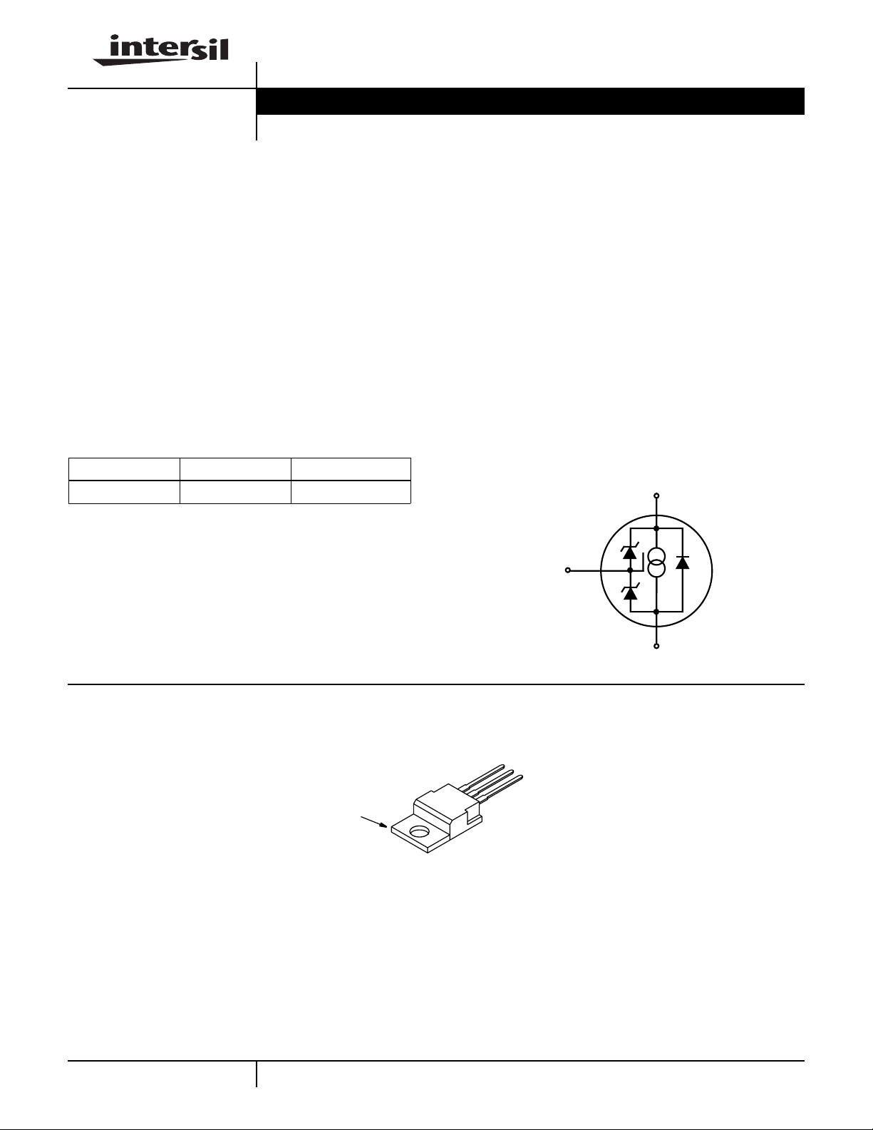
The RLP1N06CLE is an intelligent monolithic power circuit
which incorporates a lateral bipolar transistor, resistors,
zener diodes, and a PowerMOS transistor. The current
limiting of this device allows it to be used safely in circuits
where it is anticipated that a shorted load condition may be
encountered. The drain to source voltage clamping offers
precision control of the circuit voltage when switching
inductive loads. Logic level gates allow this device to be fully
biased on with only 5V from gate to source. Input protection
is provided for ESD up to 2kV.
Formerly developmental type TA09880.
Ordering Information
PART NUMBER PACKAGE BRAND
RLP1N06CLE TO-220AB L1N06CLE
NOTE: When ordering, use the entire part number.
File Number
Features
• 1A, 55V
•r
•I
• Built-in Voltage Clamp
• Built-in Current Limiting
• ESD Protected, 2kV Minimum
• Controlled Switching Limits EMI and RFI
• 175
• Logic Level Gate
• Related Literature
- TB334 “Guidelines for Soldering Surface Mount
= 0.750Ω
DS(ON)
at 150oC = 1.1A to 1.5A Maximum
LIMIT
o
C Rated Junction Temperature
Components to PC Boards”
Symbol
D
2839.4
Packaging
G
S
JEDEC TO-220AB
SOURCE
DRAIN
GATE
DRAIN (FLANGE)
6-428
CAUTION: These devices are sensitive to electrostatic discharge; follow proper ESD Handling Procedures.
http://www.intersil.com or 407-727-9207
| Copyright © Intersil Corporation 1999
Page 2
RLP1N06CLE
Absolute Maximum Ratings T
= 25oC, Unless Otherwise Specified
C
RLP1N06CLE UNITS
Drain to Source Voltage (Note 1). . . . . . . . . . . . . . . . . . . . . . . . . . . . . . . . . . . . . . . . . . . . .V
Drain to Gate Voltage (RGS = 20kΩ, Note 1). . . . . . . . . . . . . . . . . . . . . . . . . . . . . . . . . . . V
DSS
DGR
55 V
55 V
Electrostatic Voltage at TC = 25oC . . . . . . . . . . . . . . . . . . . . . . . . . . . . . . . . . . . . . . . . . . . ESD 2 kV
Continuous Drain Current . . . . . . . . . . . . . . . . . . . . . . . . . . . . . . . . . . . . . . . . . . . . . . . . . . . .I
Gate to Source Voltage (Reverse Voltage Gate Bias Not Allowed). . . . . . . . . . . . . . . . . . . .V
GS
Maximum Power Dissipation . . . . . . . . . . . . . . . . . . . . . . . . . . . . . . . . . . . . . . . . . . . . . . . . . .P
D
D
Self Limited
5.5 V
36 W
Power Dissipation Derating . . . . . . . . . . . . . . . . . . . . . . . . . . . . . . . . . . . . . . . . . . . . . . . . . . . . . 0.24 W/oC
Operating and Storage Temperature . . . . . . . . . . . . . . . . . . . . . . . . . . . . . . . . . . . . . . . TJ,T
STG
-55 to 175
Maximum Temperature for Soldering
Leads at 0.063in (1.6mm) from Case for 10s. . . . . . . . . . . . . . . . . . . . . . . . . . . . . . . . . . . . T
Package Body for 10s, See Techbrief 334 . . . . . . . . . . . . . . . . . . . . . . . . . . . . . . . . . . . . T
CAUTION: Stresses above those listed in “Absolute Maximum Ratings” may cause permanent damage to the device. This is a stress only rating and operationofthe
device at these or any other conditions above those indicated in the operational sections of this specification is not implied.
L
pkg
300
260
o
C
o
C
o
C
NOTE:
1. TJ= 25oC to 150oC.
Electrical Specifications T
= 25oC, Unless Otherwise Specified
C
PARAMETER SYMBOL TEST CONDITIONS MIN TYP MAX UNITS
Drain to Source Breakdown Voltage BV
Gate to Threshold Voltage V
Zero Gate Voltage Drain Current I
DSSID
GS(TH)VGS
DSS
= 20mA, VGS = 0V (Figure 7) 55 - 70 V
= VDS, ID = 250µA (Figure 8) 1 - 2.5 V
VDS = 45V, VGS = 0V TC = 25oC--5µA
TC = 150oC--20µA
Gate to Source Leakage Current I
GSS
VGS = 5V TC = 25oC--5µA
TC = 150oC--20µA
Drain to Source On Resistance (Note 2) r
Limiting Current I
Turn-On Time t
Turn-On Delay Time t
Rise Time t
Turn-Off Delay Time t
Fall Time t
Turn-Off Time t
Thermal Resistance Junction to Case R
Thermal Resistance Junction to Ambient R
DS(ON)ID
DS(LIM)VDS
(ON)
d(ON)
r
d(OFF)
f
(OFF)
θJC
θJA
Electrostatic Voltage ESD Human Model (100pF, 1.5kΩ)
= 1A, VGS = 5V
(Figure 6)
= 15V, VGS = 5V
(Figure 2)
VDD = 30V, ID = 1A, VGS = 5V, RGS = 25Ω
RL = 30Ω
TC = 25oC - - 0.750 Ω
TC = 150oC - - 1.500 Ω
TC = 25oC 1.8 - 3 A
TC = 150oC 0.9 - 1.5 A
- - 6.5 µs
- - 1.5 µs
1-5µs
- - 7.5 µs
1-5µs
- - 12.5 µs
- - 4.17oC/W
TO-220AA - - 62
2000 - - V
o
C/W
MIL-STD-883B (Category B2)
Source to Drain Diode Specifications
PARAMETER SYMBOL TEST CONDITIONS MIN TYP MAX UNITS
Source to Drain Diode Voltage (Note 2) V
SD
Reverse Recovery Time t
NOTES:
2. Pulsed: pulse duration = 80µs maximum, duty cycle = 2%.
3. Repetitive rating: pulse width limited by maximum junction temperature.
6-429
ISD = 1A - - 1.5 V
ISD = 1A - - 1 ms
rr
Page 3
RLP1N06CLE
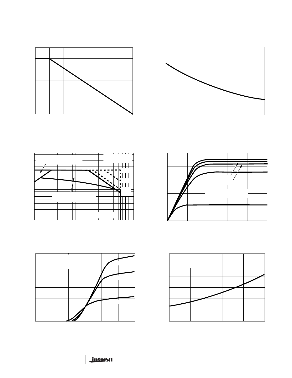
Typical Performance Curves
1.2
1.0
0.8
0.6
0.4
0.2
POWER DISSIPATION MULTIPLIER
0
0 25 50 75 100 175
TC, CASE TEMPERATURE (oC)
Unless Otherwise Specified
125
FIGURE 1. NORMALIZED POWER DISSIPATION vs CASE
TEMPERATURE
10
OPERATION IN THIS AREA
MAY BE LIMITED BY r
1
OPERATION IN THIS AREA
LIMITED BY I
, DRAIN TO SOURCE CURRENT (A)
DS
I
0.1
1 10 100
V
DS
DS(ON)
DS(LIM)
V
, DRAIN TO SOURCE VOLTAGE (V)
DSS
MAX = 55V
TJ = MAX RATED
T
= 25oC
C
150
100µs
1ms
10ms
DC
2.0
PULSE DURATION = 80µs
DUTY CYCLE = 0.5% MAX
= 10V, VGS = 5V
V
DS
1.5
1.0
0.5
NORMALIZED DRAIN CURRENT
0
-50 -25 0 25 50 75 100 125 150 175
T
, CASE TEMPERATURE (oC)
C
FIGURE 2. NORMALIZED CURRENT LIMIT vs CASE
TEMPERATURE
2.5
2.0
1.5
1.0
0.5
, DRAIN TO SOURCE CURRENT (A)
DS
I
0
012345
, DRAIN TO SOURCE VOLTAGE (V)
V
DS
VGS = 6V
= 5V
V
GS
PULSE DURATION = 80µs
DUTY CYCLE = 0.5% MAX
VGS = 7V
VGS = 4V
VGS = 3V
FIGURE 3. FORWARD BIAS SAFE OPERATING AREA FIGURE 4. SATURATION CHARACTERISTICS
3.0
VDS >> IDS x r
PULSE DURATION = 80µs
2.5
DUTY CYCLE = 0.5% MAX
2.0
1.5
1.0
, DRAIN TO SOURCE CURRENT (A)
0.5
DS(ON)
I
0
0123456
DS(ON)
, GATE TO SOURCE VOLTAGE (V)
V
GS
-25oC
25oC
150oC
3.0
VGS = 5V, ID = 0.5A
PULSE DURATION = 80µs
2.5
DUTY CYCLE = 0.5% MAX
2.0
1.5
1.0
ON RESISTANCE
0.5
NORMALIZED DRAIN TO SOURCE
0
-50 -25 0 25 50 75 100 125 150 175
, JUNCTION TEMPERATURE (oC)
T
J
FIGURE 5. TRANSFER CHARACTERISTICS FIGURE 6. NORMALIZED DRAIN TOSOURCE ON
RESISTANCE vs JUNCTION TEMPERATURE
6-430
Page 4

RLP1N06CLE
Typical Performance Curves
2.0
VGS = V
DS
ID = 250µA
1.6
1.2
0.8
0.4
0
NORMALIZED GATE THRESHOLD VOLTAGE
-50 -25 0 25 50 75 100 125 150 175
T
, JUNCTION TEMPERATURE (oC)
J
Unless Otherwise Specified (Continued)
FIGURE 7. NORMALIZED GATETHRESHOLD VOLTAGE vs
JUNCTION TEMPERATURE
300
VGS = 0V, f = 1MHz
C
= CGS + C
250
200
150
100
C, CAPACITANCE (pF)
50
0
0
C
OSS
C
ISS
5
V
DS
10
, DRAIN TO SOURCE VOLTAGE (V)
ISS
C
= C
RSS
C
≈ CDS+ C
OSS
C
RSS
15 20
GD
GD
GD
2.0
ID = 20mA
1.5
1.0
0.5
BREAKDOWN VOLTAGE
NORMALIZED DRAIN TO SOURCE
0
-50 -25 0 25 50 75 100 125 150 175
, JUNCTION TEMPERATURE (oC)
T
J
FIGURE 8. NORMALIZED DRAIN TOSOURCE BREAKDOWN
VOLTAGE vs JUNCTION TEMPERATURE
R
L
V
DS
V
GS
0V
25
V
GS
R
GS
DUT
+
-
FIGURE 9. CAPACITANCE vs DRAIN TO SOURCE VOLTAGE FIGURE 10. SWITCHING TEST CIRCUIT
25
HSTR = 0oC/W
20
15
10
, DRAIN TO SOURCE VOLTAGE (V)
DS
V
1oC/W
2oC/W
5oC/W
10oC/W
5
25oC/W
0
25 50 75 100 125 150
, AMBIENT TEMPERATURE (oC)
T
A
TJ = 175oC
I
LIM
R
θJC
FREE AIR R
= 1.35A
= 4.17oC/W
θJA
FIGURE 11. DC OPERATION IN CURRENT LIMITING
= 80oC/W
175
80
DUTY CYCLE = 20%
60
40
50%
20
, DRAIN TO SOURCE VOLTAGE (V)
MAX PULSE WIDTH = 100ms
DS
TJ = 175oC, I
V
0
25 50 75 100 125 150
= 1.35A, R
LIM
, AMBIENT TEMPERATURE (oC)
T
A
NOTE: Heatsink thermal resistance = 2
10% 5% 2%
= 4.17oC/W
θJC
o
C/W
FIGURE 12. MAXIMUM VDS vs TA IN CURRENT LIMITING
6-431
175
Page 5

RLP1N06CLE
Typical Performance Curves
80
TJ = 175oC
I
= 1.35A
LIM
= 4.17oC/W
R
θJC
60
DUTY CYCLE = 20%
40
20
, DRAIN TO SOURCE VOLTAGE (V)
DS
V
MAX PULSE WIDTH = 100ms
0
25 50 75 100 125 150
T
A
50%
, AMBIENT TEMPERATURE (oC)
Unless Otherwise Specified (Continued)
10% 5% 2%
NOTE: Heatsink thermal resistance = 5oC/W
FIGURE 13. MAXIMUM VDS vs TA IN CURRENT LIMITING
80
MAX PULSE WIDTH = 100ms
TJ = 175oC
I
= 1.35A
LIM
= 4.17oC/W
R
60
θJC
5% 2%
1%
175
80
60
40
20
, DRAIN TO SOURCE VOLTAGE (V)
DS
V
MAX PULSE WIDTH = 100ms
0
25 50 75 100 125 150
TJ = 175oC
I
= 1.35A
LIM
= 4.17oC/W
R
θJC
DUTY CYCLE = 20%
50%
, AMBIENT TEMPERATURE (oC)
T
A
5% 2%10%
NOTE: Heatsink thermal resistance = 10oC/W
FIGURE 14. MAXIMUM VDS vs TA IN CURRENT LIMITING
80
60
2%
MAX PULSE WIDTH = 100ms
TJ = 175oC
I
= 1.35A
LIM
= 80oC/W
R
θJA
DUTY CYCLE = 1%
175
40
10%
20
, DRAIN TO SOURCE VOLTAGE (V)
DS
V
DUTY CYCLE = 20%
50%
0
25 50 75 100 125 150
, AMBIENT TEMPERATURE (oC)
T
A
NOTE: Heatsink thermal resistance = 25oC/W
FIGURE 15. MAXIMUM VDS vs TA IN CURRENT LIMITING
10
8
C (s)
o
TIME TO 175
150oC
6
4
2
0
0 5 10 15 20
125oC 100oC 75oC 50oC
, DRAIN TO SOURCE VOLTAGE (V)
V
DS
STARTING
TEMP = 25oC
R
θJC
4.17
o
=
C/W
175
40
5%
20
, DRAIN TO SOURCE VOLTAGE (V)
DS
V
10%
50%
0
25 50 75 100 125 150
, AMBIENT TEMPERATURE (oC)
T
A
175
NOTE: No external heatsink
FIGURE 16. MAXIMUM VDS vs TA IN CURRENT LIMITING
10
8
125oC 100oC 75oC
150oC 50oC
C (s)
6
o
4
TIME TO 175
2
0
25
0 5 10 15 20
V
, DRAIN TO SOURCE VOLTAGE (V)
DS
STARTING
TEMP = 25oC
R
θJC
4.17
=
o
C/W
25
NOTE: Heatsink thermal resistance = 2oC/W
Heatsink thermal capacitance = 4j/oC
FIGURE 17. TIME TO 175oC IN CURRENT LIMITING
6-432
NOTE: Heatsink thermal resistance = 5oC/W
Heatsink thermal capacitance = 2j/oC
FIGURE 18. TIME TO 175oC IN CURRENT LIMITING
Page 6

RLP1N06CLE
Typical Performance Curves
10
8
150oC 50oC
C (s)
6
o
4
TIME TO 175
2
0
0 5 10 15 20
NOTE: Heatsink thermal resistance = 10oC/W
Heatsink thermal capacitance = 1j/oC
FIGURE 19. TIME TO 175oC IN CURRENT LIMITING
100oC
125oC
V
DS
75oC
, DRAIN TO SOURCE VOLTAGE (V)
STARTING
TEMP = 25
10
8
Unless Otherwise Specified (Continued)
R
=
θJC
o
C/W
4.17
o
C
25
10
8
C (s)
6
o
4
TIME TO 175
2
0
0 5 10 15 20
NOTE: Heatsink thermal resistance = 25oC/W
Heatsink thermal capacitance = 0.5j/oC
FIGURE 20. TIME TO 175oC IN CURRENT LIMITING
125oC
150oC 50oC
R
80
75oC
100oC
V
, DRAIN TO SOURCE VOLTAGE (V)
DS
=
θJA
o
C/W
STARTING
TEMP = 25
R
=
θJC
o
C/W
4.17
o
C
25
C (s)
6
o
4
TIME TO 175
2
0
0 5 10 15 20
150oC
125oC
V
, DRAIN TO SOURCE VOLTAGE (V)
DS
NOTE: No external heatsink
FIGURE 21. TIME TO 175oC IN CURRENT LIMITING
Detailed Description
Temperature Dependence of Current Limiting and
Switching Speed
The RLP1N06CLE is a monolithic power device which
incorporates a logic levelPowerMOS transistor with a resistor
in series with the source. The base and emitter of a lateral
bipolar transistor is connected across this resistor, and the
collector of the bipolar transistor is connected to the gate of
the Pow erMOS transistor. When the voltage across the
resistor reaches the value required to forward bias the emitter
base junction of the bipolar transistor, the bipolar transistor
“turns on”. A series resistor is incorporated in series with the
gate of the Pow erMOS tr ansistor allo wing the bipolar
transistor to drive the gate of the Po w erMOS tr ansistors to a
voltage which just maintains a constant current in the
Pow erMOStransistor.Since both theresistance of the resistor
75oC
100oC
STARTING
TEMP = 25
o
C
25
in series with the PowerMOS transistor source and voltage
required to forward bias the base emitter junction of the
bipolar transistor vary with the temperature, the current at
which the device limits is a function of temperature. This
dependence is shown in figure 2.
The resistor in series with the gate of the PowerMOS
transistor results in much slower switching than in most
PowerMOS transistors. This is an advantage where fast
switchingcan cause EMI or RFI. The switchingspeed is very
predictable, and a minimum as well as maximum fall time is
given in the device characteristics for this type.
DC Operation of the RLP1N06CLE
The limit of the drain to source voltage for operation in
current limiting on a steady state (DC) basis is shown as
Figure 11. The dissipation in the device is simply the applied
drain to source voltage multiplied by the limiting current. This
6-433
Page 7

RLP1N06CLE
device,like most PowerMOSFET devices today,is limited to
o
175
C. The maximum voltage allowable can, therefore be
expressed as:
175oCT
–()
V
----------------------------------------------------------=
DS
I
LIMRθJCRθCA
AMBIENT
+()×
(EQ. 1)
Duty Cycle Operation of the RLP1N06CLE
In many applications either the drain to source voltage or the
gate drive is not availab le 100% of the time . The copper
header on which the RLP1N06CLE is mounted has a very
large thermal storage capability , so for pulse widths of less
than 100 milliseconds, the temperature of the header can be
considered a constant case temperature calculated simply as:
T
VDSIDDR
C
Generally the heat storage capability of the silicon chip in a
power transistor is ignored for duty cycle calculations.
Making this assumption, limiting junction temperature to
o
175
C and using the TCcalculated above,the expression for
maximum V
V
DS
------------------------------------------=
I
LIM
DS
175 TC–
These values are plotted as Figures 12 thru 16.
×××()T
θCA
+=
AMBIENT
under duty cycle operation is:
DR
××
θJC
(EQ. 2)
(EQ. 3)
Limited Time Operations of the RLP1N06CLE
Protection for a limited period of time is sufficient for many
applications. As stated above the heat storage in the silicon
chip can usually be ignored for computations of over 10
milliseconds and the thermal equivalent circuit reduces to a
simple enough circuit to allow easy computation on the
limiting conditions. The variation in limiting current with
temperature complicates the calculation of junction
temperature, but a simple straight line approximation of the
variation is accurate enough to allow meaningful
computations. The curves shown as figures 17 thru 21 give
an accurate indication of how long the specified voltage can
be applied to the device in the current limiting mode without
exceeding the maximum specified 175
temperature. In practice this tells you how long you have to
alleviate the condition causing the current limiting to occur.
o
C junction
All Intersil semiconductor products are manufactured, assembled and tested under ISO9000 quality systems certification.
Intersil semiconductor products are sold by description only.Intersil Corporation reserves the right to make changes in circuit design and/or specifications at any time without notice. Accordingly ,the reader is cautioned to verify that data sheets are current before placing orders. Information furnished by Intersil is believed to be accurate and
reliable. However, no responsibility is assumed by Intersil or its subsidiaries for its use; nor for any infringements of patents or other rights of third parties which may result
from its use. No license is granted by implication or otherwise under any patent or patent rights of Intersil or its subsidiaries.
For information regarding Intersil Corporation and its products, see web site http://www.intersil.com
Sales Office Headquarters
NORTH AMERICA
Intersil Corporation
P. O. Box 883, Mail Stop 53-204
Melbourne, FL 32902
TEL: (407) 724-7000
FAX: (407) 724-7240
6-434
EUROPE
Intersil SA
Mercure Center
100, Rue de la Fusee
1130 Brussels, Belgium
TEL: (32) 2.724.2111
FAX: (32) 2.724.22.05
ASIA
Intersil (Taiwan) Ltd.
7F-6, No. 101 Fu Hsing North Road
Taipei, Taiwan
Republic of China
TEL: (886) 2 2716 9310
FAX: (886) 2 2715 3029
 Loading...