Page 1
RLD03N06CLE, RLD03N06CLESM,
RLP03N06CLE
Data Sheet July 1999
0.3A, 60V, 6 Ohm, ESD Rated, Current
Limited, Voltage Clamped, Logic Level
N-Channel Power MOSFETs
These are intelligent monolithic power circuits which
incorporate a lateral bipolar transistor, resistors, zener
diodes and a power MOS transistor. The current limiting of
these devices allow it to be used safely in circuits where a
shorted load condition may be encountered. The drain to
source voltage clamping offersprecisioncontrolofthecircuit
voltage when switching inductive loads. The “Logic Level”
gate allows this device to be fully biased on with only 5V
from gate to source, thereby facilitating true on-off power
control directly from logic level (5V) integrated circuits.
These devicesincorporate ESD protection andaredesigned
to withstand 2kV (Human Body Model) of ESD.
Formerly developmental type TA49028.
Ordering Information
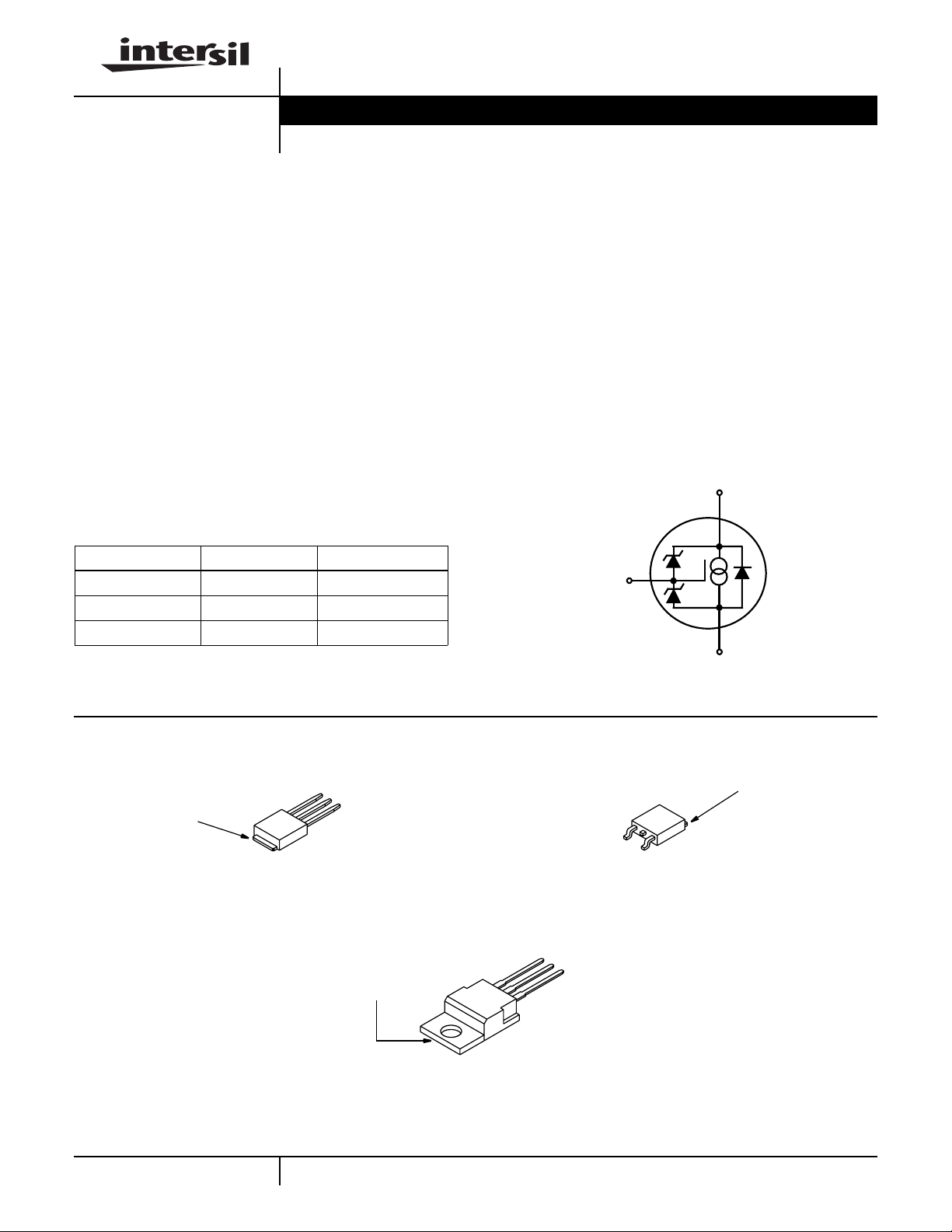
PART NUMBER PACKAGE BRAND
RLD03N06CLE TO-251AA 03N06C
RLD03N06CLESM TO-252AA 03N06C
RLP03N06CLE TO-220AB 03N06CLE
NOTE: Whenordering, usethe entire partnumber. Add the suffix9A to
obtainthe TO-252AAvariant in tape and reel,i.e. RLD03N06CLESM9A.
File Number
Features
• 0.30A, 60V
DS(ON)
= 6.0Ω
0.140 to 0.210A at 150oC
LIMIT
•r
• Built in Current Limit I
• Built in Voltage Clamp
®
• Temperature Compensating PSPICE
Model
• 2kV ESD Protected
• Controlled Switching Limits EMI and RFI
• Related Literature
- TB334 “Guidelines for Soldering Surface Mount
Components to PC Boards”
Symbol
D
G
S
3948.5
Packaging
(FLANGE)
DRAIN
JEDEC TO-251AA JEDEC TO-252AA
SOURCE
DRAIN
GATE
GATE
SOURCE
JEDEC TO-220AB
SOURCE
DRAIN
GATE
PSPICE® is a registered trademark of MicroSim Corporation.
| Copyright © Intersil Corporation 1999
6-418
DRAIN
(FLANGE)
CAUTION: These devices are sensitive to electrostatic discharge; follow proper ESD Handling Procedures.
http://www.intersil.com or 407-727-9207
DRAIN
(FLANGE)
Page 2
RLD03N06CLE, RLD03N06CLESM, RLP03N06CLE
Absolute Maximum Ratings T
= 25oC, Unless Otherwise Specified
C
RLD03N06CLE, RLD03N06CLESM,
RLP03N06CLE UNITS
Drain to Source Voltage (Note 1). . . . . . . . . . . . . . . . . . . . . . . . . . . . . . . . . . . . .V
Drain to Gate Voltage. . . . . . . . . . . . . . . . . . . . . . . . . . . . . . . . . . . . . . . . . . . . . V
Gate to Source Voltage (Reverse Voltage Gate Bias Not Allowed). . . . . . . . . . . .V
Continuous Drain Current . . . . . . . . . . . . . . . . . . . . . . . . . . . . . . . . . . . . . . . . . . . . .I
Power Dissipation . . . . . . . . . . . . . . . . . . . . . . . . . . . . . . . . . . . . . . . . . . . . . . . . . . P
DSS
DGR
GS
D
D
Derate Above 25oC . . . . . . . . . . . . . . . . . . . . . . . . . . . . . . . . . . . . . . . . . . . . . . . . .
Electrostatic Discharge Rating MIL-STD-883, Category B(2) . . . . . . . . . . . . . . . .ESD 2 KV
Operating and Storage Temperature . . . . . . . . . . . . . . . . . . . . . . . . . . . . . . . TJ, T
STG
Maximum Temperature for Soldering
Leads at 0.063in (1.6mm) from Case for 10s. . . . . . . . . . . . . . . . . . . . . . . . . . . . T
Package Body for 10s, See Techbrief 334 . . . . . . . . . . . . . . . . . . . . . . . . . . . . .T
CAUTION: Stresses above those listed in “Absolute Maximum Ratings” may cause permanent damage to the device. This is a stress only rating and operationofthe
device at these or any other conditions above those indicated in the operational sections of this specification is not implied.
L
pkg
60 V
60 V
+5.5 V
Self Limited
30
0.2
-55 to 175
300
260
W
W/oC
o
C
o
C
o
C
NOTE:
1. TJ= 25oC to 150oC.
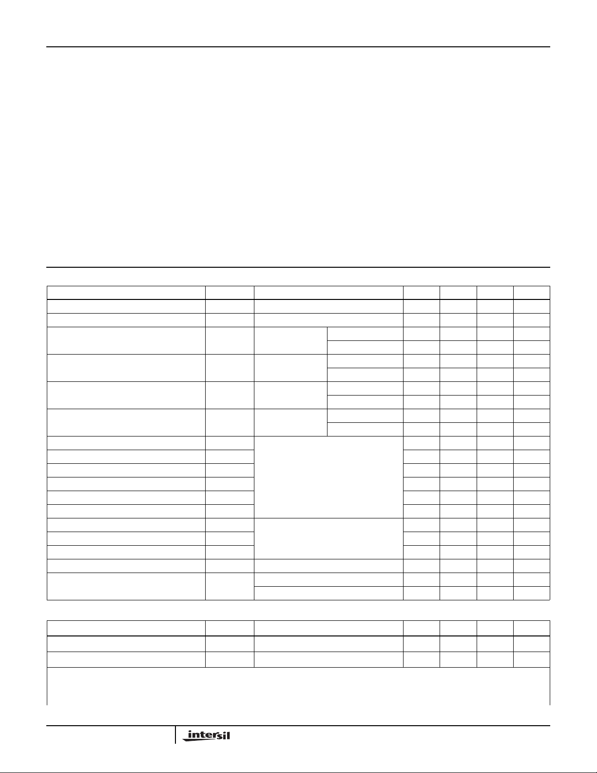
Electrical Specifications T
= 25oC, Unless Otherwise Specified
C
PARAMETER SYMBOL TEST CONDITIONS MIN TYP MAX UNITS
Drain to Source Breakdown Voltage BV
Gate Threshold Voltage V
Zero Gate Voltage Drain Current I
Gate to Source Leakage Current I
DSSID
GS(TH)VGS
DSS
GSS
= 250µA, VGS = 0V 60 - 85 V
= VDS, ID = 250µA 1 - 2.5 V
VDS = 45V,
VGS = 0V
TJ = 25oC--25µA
TJ = 150oC - - 250 µA
VGS = 5V TJ = 25oC--5µA
TJ = 150oC--20µA
Drain to Source On Resistance (Note 2) r
Limiting Current I
DS(ON)ID
DS(LIMIT)VDS
Turn-On Time t
Turn-On Delay Time t
d(ON)
Rise Time t
Turn-Off Delay Time t
d(OFF)
Fall Time t
Turn-Off Time t
Input Capacitance C
Output Capacitance C
Reverse Transfer Capacitance C
Thermal Resistance Junction to Case R
Thermal Resistance Junction to Ambient R
ON
r
f
OFF
ISS
OSS
RSS
θ
θ
JC
JA
= 0.100A,
VGS = 5V
= 15V,
VGS = 5V
VDD = 30V, ID = 0.10A,
RL = 300Ω, VGS = 5V,
RGS = 25Ω
TJ = 25oC - - 6.0 Ω
TJ = 150oC - - 12.0 Ω
TJ = 25oC 280 - 420 mA
TJ = 150oC 140 - 210 mA
- - 7.5 µs
- - 2.5 µs
- - 5.0 µs
- - 7.5 µs
- - 5.0 µs
- - 12.5 µs
VDS = 25V, VGS = 0V,
f = 1MHz
- 100 - pF
-65-pF
- 3.0 - pF
- - 5.0
TO-220 Package - - 80
TO-251 and TO-252 Packages - - 100
o
o
o
C/W
C/W
C/W
Source to Drain Diode Specifications
PARAMETER SYMBOL TEST CONDITIONS MIN TYP MAX UNITS
Source to Drain Diode Voltage V
SD
Diode Reverse Recovery Time t
NOTES:
2. Pulsed: pulse duration = ≤ 300µs maximum, duty cycle = ≤ 2%.
3. Repititive rating: pulse width limited by maximum junction temperature.
6-419
ISD = 0.1A - - 1.5 V
ISD = 0.1A, dISD/dt = 100A/µs - - 1.0 ms
rr
Page 3
RLD03N06CLE, RLD03N06CLESM, RLP03N06CLE
Typical Performance Curves
1.2
1.0
0.8
0.6
0.4
0.2
POWER DISSIPATION MULTIPLIER
0
25 50 75 100 125 150 1750
0
TC, CASE TEMPERATURE (oC)
Unless Otherwise Specified
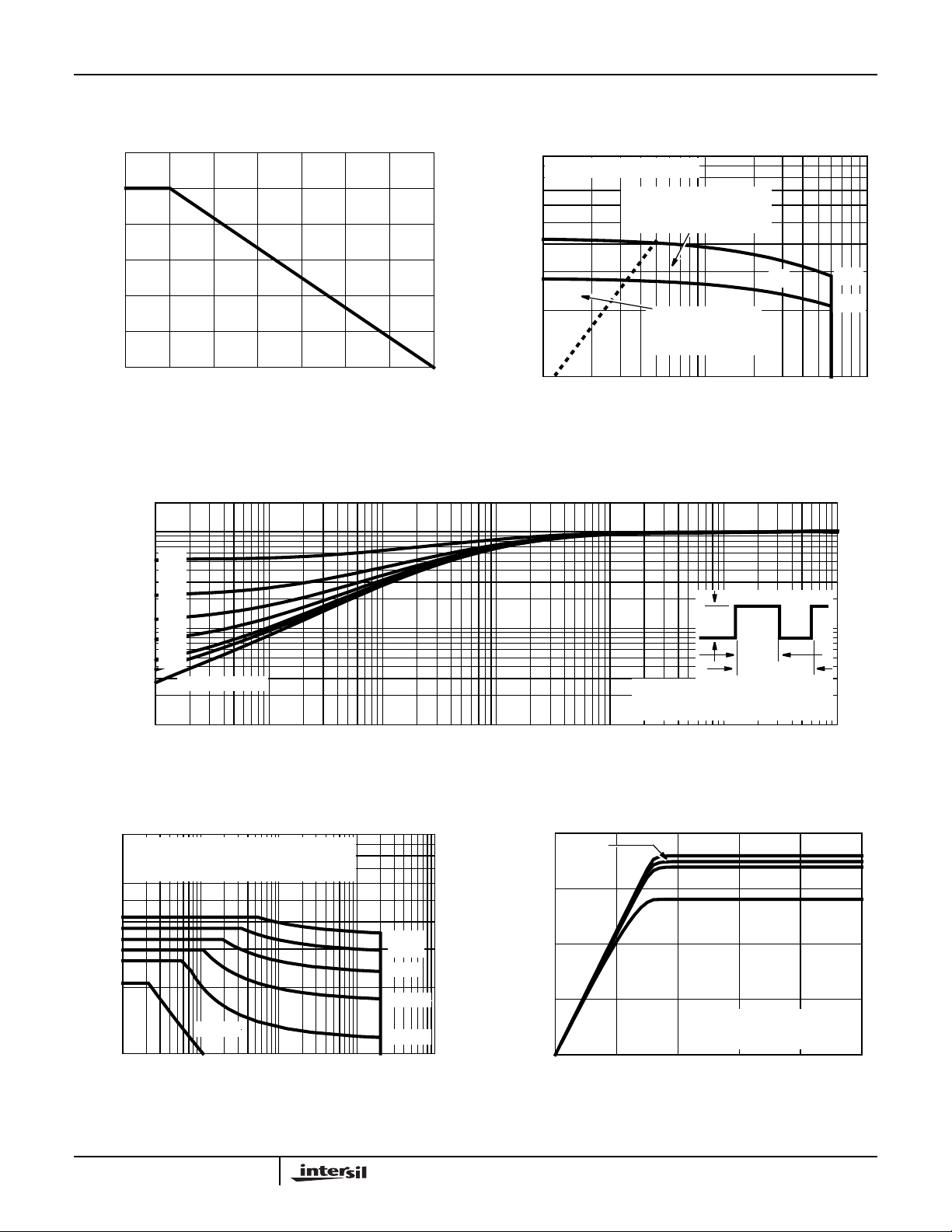
FIGURE 1. NORMALIZEDPOWER DISSIPATION vs CASE
TEMPERATURE
2
1
1
TC = 25oC, TJ = MAX RATED
OPERATION IN THIS
AREA IS LIMITED BY
JUNCTION TEMPERATURE
DC
, DRAIN CURRENT (A)
D
I
0.1
1 10 100
VDS, DRAIN TO SOURCE VOLTAGE (V)
OPERATION IN THIS
AREA MAY BE
LIMITED BY r
DS(ON)
FIGURE 2. FORWARD BIAS SAFE OPERATING AREA
25oC
175oC
0.5
0.2
0.1
0.1
, NORMALIZED
JC
θ
Z
1
, CLAMPED DRAIN CURRENT (A)
(CLAMP)
I
0.1
0.001
0.05
0.02
0.01
THERMAL IMPEDANCE
SINGLE PULSE
0.01
-5
10
= 25oC
T
C
TEMPERATURES LISTED ARE STARTING
JUNCTION TEMPERATURES
150oC
0.01 0.1 1 10
tAV, TIME IN CLAMP (s)
NOTES:
DUTY FACTOR: D = t1/t
PEAK TJ = PDM x Z
-4
10
-3
10
t, RECTANGULAR PULSE DURATION (s)
-2
10
-1
10
FIGURE 3. NORMALIZED MAXIMUM TRANSIENT THERMAL IMPEDANCE
0.40
VGS = 5V
0.30
25oC
50oC
75oC
100oC
125oC
0.20
, DRAIN CURRENT (A)
D
0.10
I
0
012345
VDS, DRAIN TO SOURCE VOLTAGE (V)
P
DM
t
1
t
2
2
x R
JC
θ
= 7.5V
+ T
JC
θ
0
10
V
GS
PULSE DURATION = 80µs
DUTY CYCLE = 0.5% MAX
= 25oC
T
C
C
10
= 4V
V
GS
VGS = 3V
1
FIGURE 4. SELF-CLAMPED INDUCTIVE SWITCHING FIGURE 5. SATURATION CHARACTERISTICS
6-420
Page 4

RLD03N06CLE, RLD03N06CLESM, RLP03N06CLE
Typical Performance Curves
0.60
0.50
0.40
0.30
0.20
, ON STATE DRAIN CURRENT (A)
0.10
D(ON)
I
= 15V
V
DD
PULSE TEST
PULSE DURATION = 80µs
DUTY CYCLE = 0.5% MAX
0
023451
, GATE TO SOURCE VOLTAGE (V)
V
GS
FIGURE 6. TRANSFER CHARACTERISTICS FIGURE 7. NORMALIZEDDRAIN TOSOURCE ON
2.0
1.5
VGS= VDS,
I
= 250µA
D
Unless Otherwise Specified (Continued)
-55oC
25oC
175
o
C
2.5
2.0
1.5
1.0
ON RESISTANCE
0.5
NORMALIZED DRAIN TO SOURCE
0
-80 -40 0 40 80 120 160 200
2.0
1.5
PULSE DURATION = 80µs
DUTY CYCLE = 0.5% MAX
V
ID = 0.10A
= 5V,
GS
TJ, JUNCTION TEMPERATURE (oC)
RESISTANCE vs JUNCTION TEMPERATURE
ID = 10mA
1.0
NORMALIZED GATE
0.5
THRESHOLD VOLTAGE
0
-80 -40 0 40 80 120 200160
TJ, JUNCTION TEMPERATURE (oC)
FIGURE 8. NORMALIZEDGATETHRESHOLD VOLTAGE vs
JUNCTION TEMPERATURE
300
200
100
C, CAPACITANCE (pF)
0
0 5 10 15 20 25
VDS, DRAIN TO SOURCE VOLTAGE (V)
VGS = 0V, f = 1MHz
= CGS + C
C
C
C
ISS
RSS
OSS
C
C
C
OSS
RSS
= C
≈ CDS + C
ISS
GD
GD
GD
1.0
0.5
NORMALIZED DRAIN TO
SOURCE BREAKDOWN VOLTAGE
0
-80 -40 0 40 80 120 160 200
TJ, JUNCTION TEMPERATURE (oC)
FIGURE 9. NORMALIZEDDRAIN TOSOURCE BREAKDOWN
VOLTAGE vs TEMPERATURE
2.0
1.5
1.0
0.5
0
NORMALIZED DRAIN LIMITING CURRENT
-80 -40 0 40 80 120 160 200
TJ, JUNCTION TEMPERATURE (oC)
VGS = 5V
PULSE DURATION = 80µs
DUTY CYCLE = 0.5% MAX.
FIGURE 10. CAPACITANCE vs DRAIN TO SOURCE VOLTAGE FIGURE 11. NORMALIZEDDRAIN LIMITING CURRENTvs
JUNCTION TEMPERATURE
6-421
Page 5

RLD03N06CLE, RLD03N06CLESM, RLP03N06CLE
Typical Performance Curves
60
45
30
15
, DRAIN SOURCE VOLTAGE (V)
DS
V
NOTE: Refer to Intersil Application Notes AN7254 and AN7260.
FIGURE 12. NORMALIZED SWITCHING WAVEFORMS FOR CONSTANT GATE CURRENT.
Test Circuits and Waveforms
V
Unless Otherwise Specified (Continued)
0
DD
R
L
I
G REF()
--------------------- -
10
I
G ACT()
VDD = BV
0.75 BV
0.50 BV
0.25 BV
t, TIME (µs)
V
DS
DSS
DSS
DSS
DSS
40
V
DS
RL = 600Ω
I
= 0.1mA
G(REF)
V
= 5V
GS
I
G REF()
--------------------- -
I
G ACT()
t
d(ON)
90%
5.00
3.75
2.50
1.25
, GATE SOURCE VOLTAGE (V)
GS
V
0.00
t
ON
t
r
t
d(OFF)
t
OFF
t
f
90%
V
0V
GS
DUT
V
R
GS
GS
10%
10%
PULSE WIDTH
FIGURE 13. RESISTIVE SWITCHING TEST CIRCUIT FIGURE 14. RESISTIVE SWITCHING WAVEFORMS
Detailed Description
Temperature Dependence of Current Limiting and
Switching Speed Performance
The RLD03N06CLE, CLESM and RLP03N06CLE are
monolithic power deviceswhich incorporateaLogicLev elpower
MOSFET transistor with a current sensing scheme and control
circuitry to enable the device to self limit the drain source current
flow . The current sensing scheme supplies current to a resistor
thatisconnected across thebase to emitter ofa bipolar transistor
in the control section. The collector of this bipolar transistor is
connected to the gate of the power MOSFET transistor . When
the ratiometric current from the current sensing reaches the
value required to forward bias the base emitter junction of this
bipolar transistor ,the bipolar “turns on”. A resistor isincorporated
in series with the gate of the power MOSFET transistor allowing
the bipolar transistor to adjust the drive on the gate of the power
MOSFET transistortoa voltage which then maintains a constant
current in the power MOSFET transistor . Since both the
ratiometric current sensing schemeandthebase emitter unction
voltageof the bipolartransistorvary with temperature,the current
at which the device limits is a function of temperature. This
dependence is shown in Figure 3.
The resistor in series with the gate of the power MOSFET
transistor also results in much slower switching performance
than in standard power MOSFET transistors. This is an
advantage where fast switching can cause EMI or RFI. The
switching speed is very predictable.
DC Operation
The limit on the drain to source voltage for operation in
current limiting on a steady state (DC) basis is shown in the
equation below. The dissipation in the device is simply the
applied drain to source voltage multiplied by the limiting
current. This device, like most power MOSFET devices
today, is limited to 175
can, therefore, be expressed as shown in Equation 1:
150°CT
–()
-------------------------------------------------------=
DS
I
LM RθJC RθJA+()•
AMBIENT
o
C. The maximum voltage allowable
10%
90%
50%50%
(EQ.1)
6-422
Page 6

RLD03N06CLE, RLD03N06CLESM, RLP03N06CLE
The results of this equation are plotted in Figure 15 for various
heatsinks.
Duty Cycle Operation
In many applications either the drain to source voltage or the
gate drive isnotav ailab le100% of the time. The copper header
on which the RLD03N06CLE, CLESM and RLP03N06CLE is
mounted has a very large thermal storage capability , so f or
pulse widths of less then 1ms, the temperature of the header
can beconsidereda constant, thereby thejunctiontemperature
can be calculated simply as shown in Equation 2:
T
VDSID• D• R
C
•()T
θCA
+=
AMBIENT
(EQ.2)
Generally the heat storage capability of the silicon chip in a
power transistor is ignored for duty cycle calculations . Making
this assumption, limiting junction temperature to 175
using the T
ximum V
:
V
DS
calculated in Equation 2, the expression for ma-
C
under duty cycle operation is shown in Equation 3
DS
o
150 C TC–
----------------------------------------- -=
I
DR
••
LM
θJC
o
C and
(EQ.3)
Typical Performance Curves
90
75
HSTR = 5oC/W
60
HSTR = 10oC/W
45
HSTR = 0oC/W
HSTR = 1
HSTR = 2oC/W
TJ = 175oC
I
R
= 0.210A
LIM
JC
θ
o
C/W
= 5.0oC/W
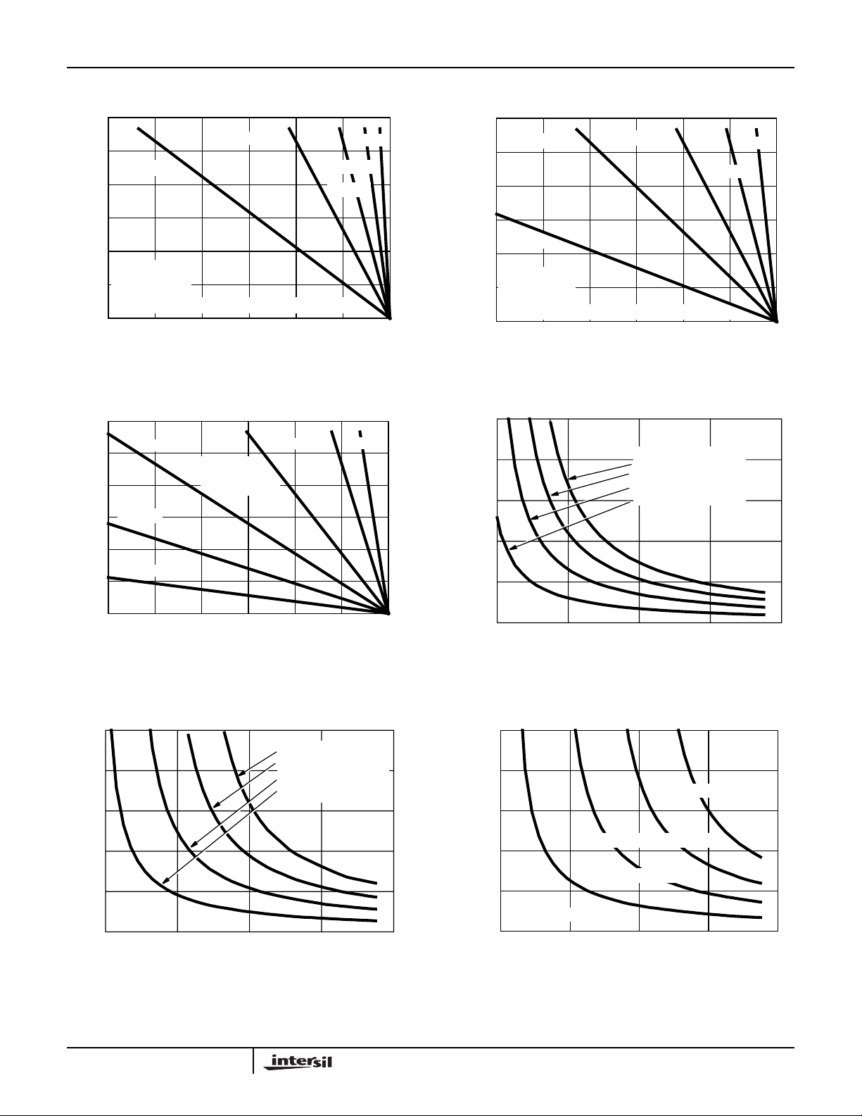
These values are plotted as Figures 16 through 21 for various heatsink thermal resistances.
Limited Time Operations
Protection for a limited period of time is sufficient for many
applications. As stated above the heat storage in the silicon
chip can usually be ignored for computations of over 10 ms ,
thereby the thermal equivalent circuit reduces to a simple
enough circuit to allow easy computation on the limiting
conditions. The variation in limiting current with temperature
complicates the calculation of junction temperature, but a
simple straight line approximation of the variation is accurate
enough to allow meaningful computations. The curves shown
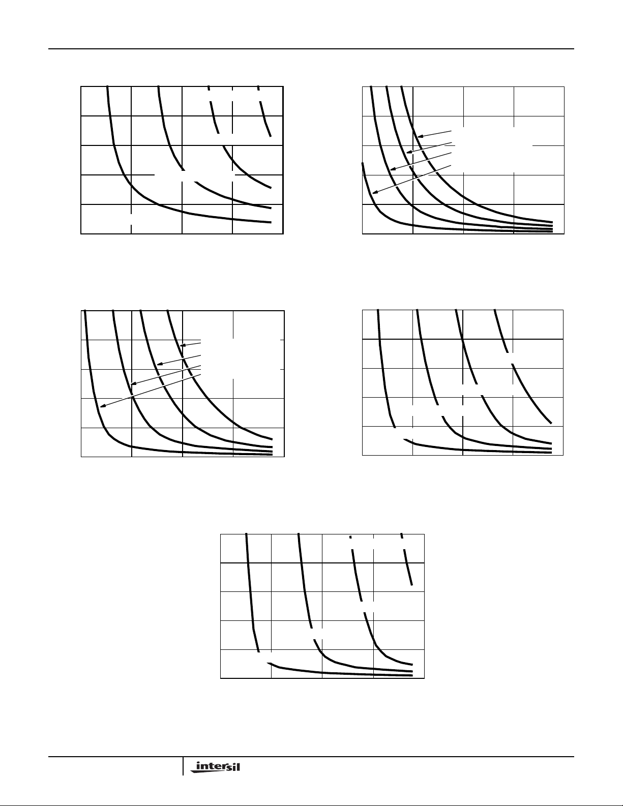
as Figures 22 through 25 (RLP03N06CLE) and Figure 26
through 29 (RLD03N06CLE and RLD03N06CLESM) give an
accurate indication of how long the specified voltage can be
applied to the device in the current limiting mode without
exceedingthe maximum specified 175
In practice this tells you how long you ha v e to alleviate the
condition causing the current limiting to occur.
90
DC = 50%
75
60
45
o
C junctiontemperature.
DC = 20%
DC = 2%
DC = 5%
DC = 10%
30
, APPLIED VOLTAGE (V)
HSTR = 25oC/W
DS
V
15
HSTR = 80oC/W
0
25 50 75 100 125 150 175
, AMBIENT TEMPERATURE (oC)
T
A
NOTE: Heat Sink Thermal Resistance = HSTR.
FIGURE 15. DC OPERATION IN CURRENT LIMITING
90
75
DC = 50%
60
45
30
TJ = 175oC
= 0.210A
I
, DRAIN TO SOURCE VOLTAGE (V)
DS
V
LIM
15
R
= 5.0oC/W
JC
θ
DUTY CYCLE = DC MAX PULSE WIDTH = 100ms
0
100 125 150 175
T
, AMBIENT TEMPERATURE (oC)
A
DC = 20%
DC = 2%
DC = 5%
DC = 10%
FIGURE 17. MAXIMUMVDSvs AMBIENT TEMPERATURE IN
CURRENT LIMITING. (HSTR = 2oC/W)
30
TJ = 175oC
I
= 0.210A
, DRAIN TO SOURCE VOLTAGE (V)
15
DS
V
0
100 125 150 175
LIM
= 5.0oC/W
R
JC
θ
DUTY CYCLE = DC MAX PULSE WIDTH = 100ms
T
, AMBIENT TEMPERATURE (oC)
A
FIGURE 16. MAXIMUM VDS vs AMBIENT TEMPERATURE IN
CURRENT LIMITING. (HEATSINK THERMAL
RESISTANCE = 1oC/W)
90
75
60
DC = 50%
45
30
TJ = 175oC
= 0.210A
I
LIM
, DRAIN TO SOURCE VOLTAGE (V)
15
DS
V
= 5.0oC/W
R
JC
θ
DUTY CYCLE = DC MAX PULSE WIDTH = 100ms
0
75 100 125 150 175
T
, AMBIENT TEMPERATURE (oC)
A
DC = 20%
DC = 2%
DC = 5%
DC = 10%
FIGURE 18. MAXIMUMVDSvs AMBIENT TEMPERATURE IN
CURRENT LIMITING. (HSTR = 5oC/W)
6-423
Page 7
RLD03N06CLE, RLD03N06CLESM, RLP03N06CLE
Typical Performance Curves
90
DC = 20%
75
DC = 50%
60
45
30
TJ = 175oC
I
= 0.210A
LIM
, DRAIN TO SOURCE VOLTAGE (V)
15
R
= 5.0oC/W
JC
θ
DS
DUTY CYCLE = DC MAX PULSE WIDTH = 100ms
V
0
5025
75 100 125 150 175
, AMBIENT TEMPERATURE (oC)
T
A
(Continued)
DC = 2%
DC = 5%
DC = 10%
FIGURE 19. MAXIMUMVDSvs AMBIENT TEMPERATURE IN
CURRENT LIMITING. (HSTR = 10oC/W)
90
75
60
45
30
, DRAIN TO SOURCE VOLTAGE (V)
15
DS
V
0
DC = 10%
DC = 20%
DC = 50%
DC = 5%
TJ = 175oC
= 0.210A
I
LIM
R
= 5.0oC/W
JC
θ
5025
75 100 125 150 175
, AMBIENT TEMPERATURE (oC)
T
A
DC = 2%
DC = 1%
NOTE: Duty Cycyle = DC, Max Pulse Width = 100ms.
FIGURE 21. MAXIMUMVDSvs AMBIENT TEMPERATURE IN
CURRENT LIMITING. (HSTR = 80oC/W)
90
75
60
45
30
, DRAIN TO SOURCE VOLTAGE (V)
15
DS
V
0
DC = 20%
DC = 50%
TJ = 175oC
I
= 0.210A
LIM
= 5.0oC/W
R
JC
θ
DUTY CYCLE = DC MAX PULSE WIDTH = 100ms
5025
75 100 125 150 175
, AMBIENT TEMPERATURE (oC)
T
A
DC = 10%
DC = 2%
DC = 5%
FIGURE 20. MAXIMUMVDSvs AMBIENT TEMPERATURE IN
CURRENT LIMITING. (HSTR = 25oC/W)
10
STARTING TJ = 75oC
STARTING T
STARTING T
STARTING T
50 70 903010
= 100oC
J
= 125oC
J
= 150oC
J
C (s)
o
TIME TO 175
8
6
4
2
0
VDS, DRAIN TO SOURCE VOLTAGE (V)
FIGURE 22. TIME TO 175oC IN CURRENT LIMITING
(HEATSINK THERMAL RESISTANCE = 25oC/W)
(HEATSINK THERMAL CAPACITANCE = 0.5J/oC)
10
STARTING TJ = 75oC
STARTING T
STARTING T
STARTING T
50 70 903010
C (s)
o
TIME TO 175
8
6
4
2
0
VDS, DRAIN TO SOURCE VOLTAGE (V)
FIGURE 23. TIME TO 175oC IN CURRENT LIMITING
(HEATSINK THERMAL RESISTANCE = 10oC/W)
(HEATSINK THERMAL CAPACITANCE = 1.0J/oC)
6-424
= 100oC
J
= 125oC
J
= 150oC
J
10
8
C (s)
o
TIME TO 175
6
4
2
STARTING TJ = 150oC
0
STARTING TJ = 100oC
STARTING TJ = 125oC
3010
VDS, DRAIN TO SOURCE VOLTAGE (V)
STARTING TJ = 75oC
50 70 90
FIGURE 24. TIME TO 175oC IN CURRENT LIMITING
(HEATSINK THERMAL RESISTANCE = 5oC/W)
(HEATSINK THERMAL CAPACITANCE = 2.0J/oC)
Page 8
RLD03N06CLE, RLD03N06CLESM, RLP03N06CLE
Typical Performance Curves
10
8
C (s)
o
TIME TO 175
6
4
2
STARTING TJ = 150oC
0
VDS, DRAIN TO SOURCE VOLTAGE (V)
STARTING TJ = 100oC
STARTING TJ = 125oC
50 70 903010
(Continued)
STARTING TJ = 75oC
FIGURE 25. TIME TO 175oC IN CURRENT LIMITING
(HEATSINK THERMAL RESISTANCE = 2oC/W)
(HEATSINK THERMAL CAPACITANCE = 4J/oC)
10
C (s)
o
TIME TO 175
8
6
4
2
STARTING TJ = 75oC
STARTING TJ = 100oC
STARTING T
STARTING T
= 125oC
J
= 150oC
J
10
8
C (s)
o
TIME TO 175
6
4
2
0
VDS, DRAIN TO SOURCE VOLTAGE (V)
STARTING TJ = 75oC
STARTING TJ = 100oC
STARTING T
STARTING TJ = 150oC
50 70 903010
= 125oC
J
FIGURE 26. TIME TO 175oC IN CURRENT LIMITING
(HEATSINK THERMAL RESISTANCE = 25oC/W)
(HEATSINK THERMAL CAPACITANCE = 0.5J/oC)
10
8
C (s)
o
TIME TO 175
6
4
2
STARTING TJ = 150oC
STARTING TJ = 100oC
STARTING TJ = 125oC
STARTING TJ = 75oC
0
3010
VDS, DRAIN TO SOURCE VOLTAGE (V)
50 70 90
FIGURE 27. TIME TO 175oC IN CURRENT LIMITING
(HEATSINK THERMAL RESISTANCE = 10oC/W)
(HEATSINK THERMAL CAPACITANCE = 1.0J/oC)
10
8
C (s)
o
6
4
TIME TO 175
2
STARTING TJ = 150oC
0
FIGURE 29. TIME TO 175oC IN CURRENT LIMITING
(HEATSINK THERMAL RESISTANCE = 2oC/W)
(HEATSINK THERMAL CAPACITANCE = 4J/oC)
0
FIGURE 28. TIME TO 175oC IN CURRENT LIMITING
(HEATSINK THERMAL RESISTANCE = 5oC/W)
(HEATSINK THERMAL CAPACITANCE = 2.0J/oC)
STARTING TJ = 75oC
STARTING TJ = 100oC
STARTING TJ = 125oC
3010
VDS, DRAIN TO SOURCE VOLTAGE (V)
50 70 90
3010
VDS, DRAIN TO SOURCE VOLTAGE (V)
50 70 90
6-425
Page 9

RLD03N06CLE, RLD03N06CLESM, RLP03N06CLE
PSPICE Electrical Model
SUBCKT RLD03N06CLE 2 1 3; rev 4/18/94
CA 12 8 0.547e-9
CB 15 14 0.547e-9
CIN 6 8 0.301e-9
DBODY 7 5 DBDMOD
DBREAK 5 11 DBKMOD
DESD1 91 9 DESD1MOD
DBREAK
DPLCAP
10
DESD2 91 7 DESD2MOD
DPLCAP 10 5 DPLCAPMOD
EBREAK 11 20 17 18 66.5
EDS 14 8 5 8 1
EGS 13 8 6 8 1
ESG 6 10 6 8 1
EVTO 20 6 18 8 1
IT 8 17 1
LDRAIN 2 5 1e-9
LGATE 1 9 2.96e-9
LSOURCE 3 7 2.96e-9
GATE
1
DESD1
DESD2
LGATE
EBREAK
RGATE
9
91
11
17
18
+
EVTO
+
18
ESG
6
8
+
8
VTO
-
R
IN
MOS1 16 6 8 8 MOSMOD M = 0.99
MOS2 16 21 8 8 MOSMOD M = 0.01
QCONTROL 20 70 7 QMOD 1
RBREAK 17 18 RBKMOD 1
RDRAIN 5 16 RDSMOD 1.123
RGATE 9 20 3200
RIN 6 8 1e9
RSOURCE1 8 70 RDSMOD 1.12
RSOURCE2 70 7 RSMOD 2.16
S1A
12
13
S1B
CA CB
EGS
S2A
14
8
13
S2B
13
+
6
8
15
EDS
RVTO 18 19 RVTOMOD 1
S1A 6 12 13 8 S1AMOD
S1B 13 12 13 8 S1BMOD
S2A 6 15 14 13 S2AMOD
S2B 13 15 14 13 S2BMOD
VBAT 8 19 DC 1
VTO 21 6 0.22
.MODEL DBDMOD D (IS = 7.97e-17 RS = 1.82 TRS1 = 3.91e-3 TRS2 = 1.24e-5 CJO = 3.00e-10 TT = 1.83e-7)
.MODEL DBKMOD D (RS = 3150 TRS1 =0 TRS2 = 0)
.MODEL DESD1MOD D (BV = 13.54 TBV1 = 0 TBV2 = 0 RS = 45.5 TRS1 = 0 TRS2 = 0)
.MODEL DESD2MOD D (BV = 11.46 TBV1 = -7.576e-4 TBV2 = -3.0e-6 RS = 0 TRS1 = 0 TRS2 = 0)
.MODEL DPLCAPMOD D (CJO = 74.2e-12 IS = 1e-30 N = 10)
.MODEL MOSMOD NMOS (VTO = 1.67 KP = 3.40 IS = 1e-30 N = 10 TOX = 1 L = 1u W = 1u)
.MODEL QMOD NPN (BF =5)
.MODEL RBKMOD RES (TC1 = 4e-4 TC2 = 1.13e-8)
.MODEL RDSMOD RES (TC1 = 6.80e-3 TC2 = 6.5e-6)
.MODEL RSMOD RES (TC1 = 2.95e-3 TC2 = -1e-6)
.MODEL RVTOMOD RES (TC1 = -2.22e-3 TC2 = -1.95e-6)
.MODEL S1AMOD VSWITCH (RON = 1e-5 ROFF = 0.1 VON = -3 VOFF = -1)
.MODEL S1BMOD VSWITCH (RON = 1e-5 ROFF = 0.1 VON = -1 VOFF = -3)
.MODEL S2AMOD VSWITCH (RON = 1e-5 ROFF = 0.1 VON = -2.85 VOFF = 2.15)
.MODEL S2BMOD VSWITCH (RON = 1e-5 ROFF = 0.1 VON = 2.15 VOFF = -2.85)
.ENDS
NOTE: For further discussion of the PSPICE model consult A New PSPICE Sub-Circuit for the Power MOSFET Featuring Global
Temperature Options; IEEE Power Electronics Specialist Conference Records 1991.
+
6
C
16
IN
8
+
5
RDRAIN
21
MOS1
RSOURCE1
14
5
8
MOS2
RSOURCE2
70
LDRAIN
DBODY
LSOURCE
7
RBREAK
17
IT
DRAIN
2
3
SOURCE
18
RVTO
19
VBAT
+
All Intersil semiconductor products are manufactured, assembled and tested under ISO9000 quality systems certification.
Intersil semiconductor products are sold by description only .Intersil Corporation reserves the right to makechanges in circuit design and/or specifications at any time without notice. Accordingly, the reader is cautioned to verify that data sheets are current before placing orders. Information furnished by Intersil is believed to be accurate and
reliable. Howe ver, no responsibility is assumed by Intersil or its subsidiaries for its use; nor for any infringements of patents or other rights of third parties which may result
from its use. No license is granted by implication or otherwise under any patent or patent rights of Intersil or its subsidiaries.
For information regarding Intersil Corporation and its products, see web site http://www.intersil.com
6-426
 Loading...