

Page 1

RK2918 Datasheet Rev 1.0
RK2918 Datasheet
Preliminary
Revision 1.0
Jan. 2011
Rockchips Confidential 1
Page 2
RK2918 Datasheet Rev 1.0
Date
Revision
Description
2011-1-9
1.0
Initial Release
Revision History
Rockchips Confidential 2
Page 3

RK2918 Datasheet Rev 1.0
Table of Content
Table of Content ............................................................................................... 3
Figure Index .................................................................................................... 4
Table Index ..................................................................................................... 5
Chapter 1 Introduction .................................................................................... 6
1.1 Features ........................................................................................... 6
1.1.1 Microprocessor .......................................................................... 6
1.1.2 Memory Organization ................................................................. 7
1.1.3 Internal Memory ........................................................................ 7
1.1.4 External Memory or Storage device .............................................. 7
1.1.5 System Component .................................................................... 9
1.1.6 Video CODEC........................................................................... 11
1.1.7 JPEG CODEC ........................................................................... 12
1.1.8 Image Enhancement ................................................................ 12
1.1.9 Graphics Engine ....................................................................... 14
1.1.10 Video IN/OUT .......................................................................... 14
1.1.11 Audio Interface ........................................................................ 16
1.1.12 Connectivity ............................................................................ 17
1.1.13 Others .................................................................................... 19
1.2 Block Diagram ................................................................................. 19
Chapter 2 Package Description ....................................................................... 21
2.1 Ball Map ......................................................................................... 21
2.2 Pin Number Order ............................................................................ 25
2.3 RK2918 power/ground IO descriptions ............................................... 30
2.3.1 RK2918 function IO descriptions ................................................ 34
2.4 IO pin name descriptions .................................................................. 49
2.4.1 RK2918 IO Type ....................................................................... 56
2.5 Package information ......................................................................... 57
2.5.1 Dimension .............................................................................. 57
Chapter 3 Electrical Specification .................................................................... 60
3.1 Absolute Maximum Ratings ............................................................... 60
3.2 Recommended Operating Conditions .................................................. 60
3.3 DC Characteristics ........................................................................... 61
3.4 Electrical Characteristics for General IO .............................................. 62
3.5 Electrical Characteristics for PLL ........................................................ 63
3.6 Electrical Characteristics for SAR-ADC ................................................ 64
3.7 Electrical Characteristics for USB OTG/Host2.0 Interface ....................... 64
3.8 Electrical Characteristics for USB Host1.1 Interface .............................. 65
3.9 Electrical Characteristics for DDR IO ................................................... 65
3.10 Electrical Characteristics for eFuse ................................................ 65
Chapter 4 Hardware Guideline ........................................................................ 66
4.1 Reference design for RK2918 oscillator PCB connection ........................ 66
4.2 Reference design for PLL PCB connection ............................................ 66
4.3 Reference design for USB OTG/Host2.0 connection .............................. 67
4.4 RK2918 Power up/down sequence requirement ................................... 68
4.5 RK2918 Power on reset descriptions ................................................... 68
Rockchips Confidential 3
Page 4

RK2918 Datasheet Rev 1.0
Figure Index
Fig. 1-1 RK2918 Block Diagram ........................................................................ 20
Fig. 2-1 RK2908 Ball Mapping Diagram .............................................................. 24
Fig. 2-2 RK2908 TFBGA512 Package Top View .................................................... 58
Fig. 2-3 RK2908 TFBGA512 Package Side View ................................................... 58
Fig. 2-4 RK2908 TFBGA512 Package Bottom View ............................................... 59
Fig. 2-5 RK2908 TFBGA512 Package Dimension .................................................. 59
Fig. 4-1 External reference circuit for 24MHz/27MHz oscillators ............................. 66
Fig. 4-2 External reference circuit for 32.768KHz oscillator ................................... 66
Fig. 4-3 External reference circuit for PLL .......................................................... 67
Fig. 4-4 RK2918 USB OTG/Host2.0 interface reference connection......................... 67
Fig. 4-5 RK2918 reset signals sequence............................................................. 68
Rockchips Confidential 4
Page 5

RK2918 Datasheet Rev 1.0
Table Index
Table 2-1 RK2908 Pin Number Order Information ................................................ 25
Table 2-2 RK2918 Power/Ground IO informations................................................ 30
Table 2-3 RK2908 IO descriptions ..................................................................... 34
Table 2-4 RK2918 IO function description list ..................................................... 49
Table 2-5 RK2918 IO Type List ......................................................................... 56
Table 3-1 RK2918 absolute maximum ratings ..................................................... 60
Table 3-2 RK2918 recommended operating conditions ......................................... 60
Table 3-3 RK2918 DC Characteristics ................................................................ 61
Table 3-4 RK2918 Electrical Characteristics for Digital General IO .......................... 62
Table 3-5 RK2918 Electrical Characteristics for PLL .............................................. 63
Table 3-6 RK2918 Electrical Characteristics for SAR-ADC ...................................... 64
Table 3-7 RK2918 Electrical Characteristics for USB OTG/Host2.0 Interface............. 64
Table 3-8 RK2918 Electrical Characteristics for USB Host1.1 Interface .................... 65
Table 3-9 RK2918 Electrical Characteristics for DDR IO ........................................ 65
Table 3-10 RK2918 Electrical Characteristics for eFuse ......................................... 65
Rockchips Confidential 5
Page 6

RK2918 Datasheet Rev 1.0
Chapter 1 Introduction
RK2918 is a low power, high performance processor solution for mobile phones,
personal mobile internet device and other digital multimedia applications.
RK2918 integrates an ARM Cortex-A8 with one NEON coprocessor. Many embedded
powerful hardware accelerators provide optimized hardware performance for high-end
application. RK2918 supports almost full-format video decoder by 1080p@30fps such as
H264, H263, RMVB, MPEG2, MPEG4, VC1, AVS, VP8 etc. Also supports H.264 encoder by
1080P@30fps, high-quality JPEG encoder/decoder and special image preprocessor and
postprocessor.
Embedded 2D/3D hardware engine makes RK2918 completely compatible with
OpenGL ES2.0, OpenGL ES1.1 and OpenVG graphics standards.
RK2918 has high-performance external memory interface (DDRIII/DDRII/LPDDR)
capable of sustaining demanding memory bandwidths, also provides a complete set of
peripheral interface to support very flexible applications as follows:
2 banks, 8bits/16bits Nor Flash/SRAM interface
8 banks, 8bits/16bits Async NAND FLASH, LBA NANDN Flash, 8bits sync ONFI
NAND Flash, all embedded 24bits HW ECC
2 ranks, 2GB Memory space, 16bits/32bits DDRIII,DDRII-800,LPDDR-400
8bits HS-MMC/SD, 4bits SDIO, 8bits eMMC interface
24bits high-performance, 3-layers TFT LCD Controller with post-processor,
1920x1080 maximum display size
eBook display interface with 2048x2048 maximum resolution
8bits sensor/CCIR656 interface and 10bits/12bits Raw data interface
2ch I2S interface, 8ch I2S interface, PCM/SPDIF interface
USB OTG 2.0/USB Host2.0/ USB Host 1.0
RMII/MII interface
High-speed ADC interface, TS stream interface
8bits/16bits async modem interface
4x I2C, 4xUART with hardware flow-control , 2x SPI , PWM
This document will provide guideline on how to use RK2918 correctly and efficiently.
In them, the chapter 1 and chapter 2 will introduce the features, block diagram, and
signal descriptions and system usage of RK2918, the chapter 3 through chapter 46 will
describe the full function of each module in detail.
1.1 Features
1.1.1 Microprocessor
ARM Cortex-A8 processor is a high-performance, low-power, cached application
processor that provides full virtual memory capabilities
Full implementation of the ARM architecture v7-A instruction set
superscalar processor featuring technology for enhanced code density and
performance
Embedded NEON technology for multimedia and signal processing by executing
Advanced SIMD and VFP instruction sets
Jazelle RCT Java-acceleration technology for efficient support of ahead-of-time and
just-in-time compilation of Java and other byte code language
Thumb-2 technology for greater performance, energy efficiency and code density
TrustZone technology for secure transactions and DRM
13-stage main integer core pipeline and 10-stage NEON media core pipeline
Dynamic branch prediction with branch target address cache, global history buffer
and 8-entry return stack
MMU and separate instruction and data TLBs of 32 entries each
64-bit high-speed AXI interface supporting multiple outstanding transactions
Integrated 32KB L1 instruction cache , 32KB L1 data cache, 512KB L2 Cache with
parity and ECC check
ETM support for non-invasive debug, support JTAG and 8-wire trace interface
Rockchips Confidential 6
Page 7

RK2918 Datasheet Rev 1.0
ARMv7 debug with watchpoint and breakpoint registers and a 32-bit APB slave
interface to a coresight debug system
Four separate power domain to support Internal power switch on/off based on
different application scene(Integer core/ETM&DBG/Neon/L2 Cache)
Maximum frequency can be up to 650MHz@worst case and 1GHz@typical case
1.1.2 Memory Organization
Internal on-chip memory
10KB Boot Rom
16KB internal SRAM for security and non-security access, detailed size is
programmable
4KB internal SRAM shared with Host slave interface (HIF)
2KB internal SRAM shared with NAND controller
External off-chip memory
DDRIII, DDRII-800, 16/32bits data width, 2 ranks, 1GB(max) address space per
rank
LPDDR-400, 32bits data width, 2 ranks, 1GB(max) address space per rank
Async SRAM/Nor Flash, 8/16bits data width,2banks,1MB(max) address space
per bank
Async NAND Flash(include LBA NAND), 8/16bits data width, 8 banks
Sync DDR NAND Flash, 8bits data width, 8 banks
1.1.3 Internal Memory
①
Internal Boot Rom
Size : 10KB
Support system boot from the following device :
8bits/16bits Async NAND Flash
SPI0 interface
eMMC interface
Support system code download by the following interface:
USB OTG
UART1
Internal SRAM
Size : 16KB
Support security and non-security access
Security or non-security space is software programmable , used together with
TZMA module
Security space can be 0KB, 4KB, 8KB, 12KB, 16KB continuous size
1.1.4 External Memory or Storage device
Dynamic Memory Interface (DDRIII/DDRII/LPDDR)
Compatible with JEDEC standard DDRIII/DDRII/LPDDR SDRAM
Data rates of up to 800Mbps(400MHz) for DDRII and up to 400Mbps(200MHz)
for LPDDR
Support up to 2 ranks (chip selects), maximum 1GB address space per rank
16bits/32bits data width is software programmable
5 host ports with 64bits AXI bus interface for system access, AXI bus clock
asynchronous with DDR clock
Programmable timing parameters support DDRIII/DDRII/LPDDR SDRAM from
various vendor
Advanced command reordering and scheduling to maximize bus utilization
Low power modes, such as power-down and self-refresh for DDRII/LPDDR
SDRAM; clock stop and deep power-down for LPDDR SDRAM
Programmable ultra-high priority port(port0), typically a CPU port
Compensation for board delays and variable latencies through programmable
pipelines
Embedded dynamic drift detection in the PHY to get dynamic drift compensation
Rockchips Confidential 7
Page 8

RK2918 Datasheet Rev 1.0
with the controller
Programmable output and ODT impedance with dynamic PVT compensation
Support one low-power work mode: power down DDR PHY and most of DDR IO
except two CS and two CKE output signals, make SDRAM still in self-refresh state
to prevent data missing.
Static Memory Interface (ASRAM/Nor Flash)
Compatible with standard async SRAM or Nor Flash
Support up to 2 banks (chip selects), maximum 1MB address space per bank
For bank0, 8bits/16bits data width is software programmable; For bank1, 16bits
data width is fixed
Support separately data and address bus, also support shared data and address
bus to save IO numbers
NAND Flash Interface
Support 8bits/16bits async NAND flash, up to 8 banks
Support 8bits sync DDR NAND flash, up to 8 banks
Support LBA NAND flash in async or sync mode
16bit/1KB HW ECC, compatible with 8bit/512B
24bit/1KB HW ECC, compatible with 12bit/512B
For DDR NAND flash, support DLL bypass and 1/4 or 1/8 clock adjust, maximum
clock rate is 75MHz
For async NAND flash, support configurable interface timing , maximum data
rate is 16bit/cycle
Embedded two 256x32bits buffers to support ping-pong operation
Embedded AHB master interface to do data transfer by DMA method
Also support data transfer by AHB slave interface together with external DMAC1
eMMC Interface
Compatible with standard INAND interface
Support MMC4.2 protocol
Provide eMMC boot sequence to receive boot data from external eMMC device
One AHB slave interface to complete data transfer together with external DMAC1
or CPU
Support combined single FIFO(32x32bits) for both transmit and receive
operations
Support FIFO over-run and under-run prevention by stopping card clock
automatically
Support CRC generation and error detection
Embedded clock frequency division control to provide programmable baud rate
Support host pull-up control,card detection and initialization, write protection
Support block size from 1 to 65535Bytes
Data bus width is 8bits
SD/MMC Interface
Compatible with SD ver2.00, CE-ATA ver1.1, MMC ver4.2
One AHB slave interface to complete data transfer together with external DMAC1
or CPU
Support combined single FIFO(32x32bits) for both transmit and receive
operations
Support FIFO over-run and under-run prevention by stopping card clock
automatically
Support CRC generation and error detection
Embedded clock frequency division control to provide programmable baud rate
Support host pull-up control, card detection and initialization, write protection
Support block size from 1 to 65535Bytes
Data bus width is flexible to support 1bit/4bits for SD mode and 1bit/4bits/8bits
for MMC mode
Rockchips Confidential 8
Page 9

RK2918 Datasheet Rev 1.0
1.1.5 System Component
CRU (clock & reset unit)
Support clock gating control for individual components inside RK2918
Support soft-reset control for individual components inside RK2918
Support flexible clock solution, including clock source, clock MUX, clock
frequency division
Four embedded PLLs, source can be from two external 24MHz or 27MHz
oscillator input, also support two-level cascaded PLL to meet special clock
frequency requirement
Up to 1.6GHz clock output for ARM PLL, up to 1.0GHz clock output for another
three PLLs
PMU(power management unit)
Provide five work modes(slow mode, normal mode, idle mode, stop mode,
power-down mode) to save power by different frequency or automatically clock
gating control or power domain on/off control
Idle mode can be wakeup by any interrupt from every on-chip components or
external GPIO
Stop mode and power-down mode can be wakeup by external dedicated IO or 96
different GPIOs or RTC alarm
Provide 9 separately power domains, which can be power up/down by software
based on different application scenes
RTC
Provides Year, Month, Day, Weekday, Hours, Minutes and Seconds Information
based on 32.768KHz input clock
Programmable alarm with interrupt generation, which can be maskable
Programmable alarm to wake up external PMU device by output control pin
Provide some registers for storage system information in RK2918 power off
mode
Only need 1.2V power supply if not talk with external PMU
Timer
Four on-chip 32bits Timers with interrupt-based operation
Provide two operation modes: free-running and user-defined count
Support timer work state checkable
timer0 and timer1 are for CPU system domain, timer2 and timer3 are for peri
system domain
support independent fixed clock for timer0 and timer1 from external 24MHz
clock input, asynchronous with APB bus clock
support dependent clock for timer2 and timer3 from system, same as APB bus
clock
PWM
Four on-chip PWMs with interrupt-based operation
Programmable 4-bit pre-scalar from apb bus clock
Embedded 32-bit timer/counter facility
Support single-run or continuous-run PWM mode
Support maskable interrupt
Provides reference mode and output various duty-cycle waveform
Provides capture mode and measure the duty-cycle of input waveform
WatchDog
32 bits watchdog counter width
Counter clock is from APB bus clock
Counter counts down from a preset value to 0 to indicate the occurrence of a
timeout
Rockchips Confidential 9
Page 10

RK2918 Datasheet Rev 1.0
WDT can perform two types of operations when timeout occurs:
Generate a system reset
First generate an interrupt and if this is not cleared by the service routine by
the time a second timeout occurs then generate a system reset
Programmable reset pulse length
Totally 16 defined-ranges of main timeout period
Bus Architecture
64-bit multi-layer AXI/AHB composite bus architecture
Six embedded AXI interconnect
CPU L1 interconnect with two 64-bits AXI masters and six 32/64bits AXI
slaves
CPU L2 interconnect with one 32-bits AXI master, 32-bits AXI slave and lots
of 32-bits AHB /APB slaves
Peri interconnect with two 64-bits AXI masters, one 64-bits AXI slave, one
32-bits AXI slave, two 32-bits AHB masters and lots of 32-bits AHB/APB
slaves
Display interconnect with three 64-bits AXI masters, two 32-bits AHB
masters and one 64-bits AXI slave
GPU and VCODEC interconnect also with one 64-bits AXI master and one
64-bits AXI slave ,they are point-to-point AXI-lite architecture
For each interconnect with AXI/AHB/APB composite bus, clocks for AXI/AHB/APB
domains are always synchronous, and different integer ratio is supported for
them.
For CPU L1/CPU L2/Peri three interconnects, provide GPV registers to be
programmed by software to support different application scenes
Interrupt Controller
Support 71 interrupt sources input from different components inside RK2918 or
GPIO
Support 16 software-triggered interrupts
Two AXI slave interfaces for shared distributor and cpu to manage individual
registers with different intention
Input interrupt level is fixed , only high-level sensitive
Two interrupt output (nFIQ and nIRQ) to Cortex-A8, both are low-level sensitive
Support different interrupt priority for each interrupt source, and they are
always software-programmable
Support security extension to make some registers only be accessed in system
security mode
DMAC
Micro-code programming based DMA
The specific instruction set provides flexibility for programming DMA transfers
Linked list DMA function is supported to complete scatter-gather transfer
Support internal instruction cache
Embedded DMA manager thread
Support data transfer types with memory-to-memory, memory-to-peripheral,
peripheral-to-memory
Signals the occurrence of various DMA events using the interrupt output signals
Mapping relationship between each channel and different interrupt outputs is
software-programmable
Two embedded DMA controller , DMAC0 is for CPU system, DMAC1 is for peri
system
DMAC0 features:
6 channels totally
8 hardware request from peripherals
3 interrupt output
Dual APB slave interface for register configure, designated as secure and
Rockchips Confidential 10
Page 11

RK2918 Datasheet Rev 1.0
non-secure
Support trustzone technology and programmable secure state for each DMA
channel
DMAC1 features:
7 channels totally
20 hardware request from peripherals
4 interrupt output
Not support trustzone technology
Security system
Support trustzone technology for the following components inside RK2918
Cortex-A8, support security and non-security mode, switch by software
Interrupt controller, support some registers and dedicated interrupt sources
to work only in security mode
DMAC0, support some dedicated channels work only in security mode
eFuse, only accessed by Cortex-A8 in security mode
Internal memory , part of space is addressed only in security mode, detailed
size is software-programmable together with TZMA(trustzone memory
adapter) and TZPC(trustzone protection controller)
1.1.6 Video CODEC
Shared internal memory and bus interface for video decoder and encoder
Video Decoder
Real-time video decoder of MPEG-1, MPEG-2, MPEG-4,H.263, H.264 , AVS ,
VC-1 , RV , VP8 , Sorenson Spark
Error detection and concealment support for all video formats
Output data structure after decoder is YCbCr 4:2:0 semi-planar to have more
efficient bus usage, For H.264, YCbCr 4:0:0(monochrome) is also supported
Minimum image size is 48x48 for all video formats
H.264 up to HP level 4.2 : 1080p@60fps (1920x1088)
③
MPEG-4 up to ASP level 5 : 1080p@60fps (1920x1088)
MPEG-2 up to MP : 1080p@60fps (1920x1088)
MPEG-1 up to MP : 1080p@60fps (1920x1088)
H.263 : 576p@60fps (720x576)
Sorenson Spark : 1080p@60fps (1920x1088)
VC-1 up to AP level 3 : 1080p@30fps (1920x1088)
RV8/RV9/RV10 : 1080p@60fps (1920x1088)
VP6/VP7/VP8 : 1080p@60fps (1920x1088)
AVS : 1080p@60fps (1920x1088)
For AVS, 4:4:4 sampling not supported
For H.264, Image cropping not supported
For MPEG-4,GMC(global motion compensation) not supported
For VC-1, upscaling and range mapping are supported in image post-processor
For MPEG-4 SP/H.263/Sorenson spark, using a modified H.264 in-loop filter to
implement deblocking filter in post-processor unit
Video Encoder
Encoder only for H.264 (BP@level4.0, MP@level4.0,HP@level4.0) standard
Only support I and P slices, not B slices
Entropy encoding is CAVLC in BP and CABAC in MP
Support error resilience based on constrained intra prediction and slices
Maximum MV length is +/- 14 pixels in vertical direction and +/-30 pixels in
horizontal direction
Motion vector pixel accuracy is up to 1/4 pixels in 720p resolution and 1/2 pixels
in 1080p resolution
12 intra prediction modes
Number of reference frames is 1
Maximum number of slice groups is 1
②
Rockchips Confidential 11
Page 12

RK2918 Datasheet Rev 1.0
Input data format :
YCbCr 4:2:0 planar
YCbCr 4:2:0 semi-planar
YCbYCr 4:2:2
CbYCrY 4:2:2 interleaved
RGB444 and BGR444
RGB555 and BGR555
RGB565 and BGR565
RGB888 and BRG888
RGB101010 and BRG101010
Output data format : H.264 byte unit stream and H.264 NAL unit stream
Image size is from 96x96 to 1920x1088(Full HD)
Maximum frame rate is up to 30fps@1920x1080
Bit rate supported is from 10Kbps to 20Mbps
1.1.7 JPEG CODEC
JPEG decoder
Input JPEG file : YCbCr 4:0:0, 4:2:0, 4:2:2, 4:4:0, 4:1:1 and 4:4:4 sampling
formats
Output raw image : YCbCr 4:0:0, 4:2:0, 4:2:2, 4:4:0, 4:1:1 and 4:4:4
semi-planar
Decoder size is from 48x48 to 8176x8176(66.8Mpixels)
Maximum data rate
④
is up to 76million pixels per second
Thumbnail decoding and error detection is supported
Non-interleaved data order not supported
JPEG encoder
Input raw image :
YCbCr 4:2:0 planar
YCbCr 4:2:0 semi-planar
YCbYCr 4:2:2
CbYCrY 4:2:2 interleaved
RGB444 and BGR444
RGB555 and BGR555
RGB565 and BGR565
RGB888 and BRG888
RGB101010 and BRG101010
Output JPEG file : JFIF file format 1.02 or Non-progressive JPEG
Encoder image size up to 8192x8192(64million pixels) from 96x32
Maximum data rate
④
up to 90million pixels per second
Support thumbnail insertion with RGB8bits, RGB24bits and JPEG compressed
thumbnails
1.1.8 Image Enhancement
③
Image pre-processor
Only used together with video encoder inside RK2918 , not support stand-alone
mode
Provides RGB to YCbCr 4:2:0 color space conversion, compatible with BT.601 ,
BT.709 or user defined coefficients
Provides YCbCr4:2:2 to YCbCr4:2:0 color space conversion
Support cropping operation from 8192x8192 to any supported encoding size
Support rotation with 90 or 270 degrees
Video stabilization
Work in combined mode with video encoder inside RK2918 and stand-alone
mode
Maximum stabilization displacement in pixels for two sequential input video
Rockchips Confidential 12
Page 13

RK2918 Datasheet Rev 1.0
pictures is +/- 16 pixels
Adaptive motion compensation filter
Offset around stabilized picture is minimum 8 pixels in standalone mode and 16
pixels in combined mode
Support scene detection from video sequence, encodes key frame when scene
change noticed
Image post-processor
Combined with video/jpeg decoder, post-processor can read input data directly
from decoder output to reduce bus bandwidth
Also work as a stand-alone mode, its input data is from a camera interface or
other image data stored in external memory
Input data format :
any format generated by video decoder in combined mode
YCbCr 4:2:0 semi-planar
YCbCr 4:2:0 planar
YCbYCr 4:2:2
YCrYCb 4:2:2
CbYCrY 4:2:2
CrYCbY 4:2:2
Ouput data format:
YCbCr 4:2:0 semi-planar
YCbYCr 4:2:2
YCrYCb 4:2:2
CbYCrY 4:2:2
CrYCbY 4:2:2
Fully configurable ARGB channel lengths and locations inside 32bits, such as
ARGB 32bit(8-8-8-8),RGB 16bit(5-6-5),ARGB 16bit(4-4-4-4)
Input image size:
Combined mode : from 48x48 to 8176x8176 (66.8Mpixels)
Stand-alone mode : width from 48 to 8176,height from 48 to 8176, and
maximum size limited to 16.7Mpixels
Step size is 16 pixels
Output image size: from 16x16 to 1920x1088 (horizontal step size 8,vertical
step size 2)
Support image up-scaling :
Bicubic polynomial interpolation with a four-tap horizontal kernel and a
two-tap vertical kernel
Arbitrary non-integer scaling ratio separately for both dimensions
Maximum output width is 3x input width
Maximum output height is 3x input height, and 2.5x input height when
running RV/VP7/VP8 format decoder
Support image down-scaling:
Arbitrary non-integer scaling ratio separately for both dimensions
Unlimited down-scaling ratio
Not allowed to perform horizontal up-scaling and vertical down-scaling at the
same time
Support YCbCr to RGB color conversioin, compatible with BT.601-5 ,BT.709 and
user definable conversion coefficient
Support dithering (2x2 ordered spatial dithering for 4,5,6bit RGB channel
precision
Support programmable alpha channel and alpha blending operation with the
following overlay input formats:
8bit alpha value+YCbCr4:4:4,big endian channel order being AYCbCr, 8bits
each
8bit alpha value+24bit RGB,big endian channel order being ARGB,8bits each
Support deinterlacing with conditional spatial deinterlace filtering, only
compatible with YCbCr4:2:0 input format
Rockchips Confidential 13
Page 14

RK2918 Datasheet Rev 1.0
Support RGB image contrast / brightness / color saturation adjustment
Support image cropping & digital zoom only for JPEG or stand-alone mode
Support picture in pcture
Support image rotation (horizontal flip, vertical flip, rotation 90,180 or 270
degrees)
1.1.9 Graphics Engine
Compatible with OpenGL ES2.0 , OpenGL ES1.1, OpenVG1.1, DirectFB,
GDI/DirectDraw, EGL1.4
Support shader model3.0
Geometry rate : 60M tri/s
Depth-only Pixel rate : 600M pix/s
Textured Pixel rate : 600M pix/s
Vertex rate : 300M vert/s
2D Graphics Engine :
Bit Blit, Stretch Blit, Filter Blit
Rectangle fill and clear
Line drawing
Copy bit
Filter
High-performance stretch and shrink
Monochrome expansion for text rendering
ROP2,ROP3,ROP4 full alpha blending and transparency
Alpha blending modes including Java 2 Porter-Duff compositing blending rules,
chroma key, and pattern mask
Transparency by monochrome mask
32K x 32K raster 2D coordinate system
90,180 and 270 degrees rotation on every 2D primitive
Programmable high quality 9-tap,32-phase filter to support image scaling
Blending, scaling and rotation are supported in one pass for stretch Blit
Source format :
RGBA4444,5551,8888
RGBX4444,5551,8888
RGB565
UYVY4:2:2, YUY2(4:2:2),YV12(4:2:0)
Destination formats :
RGBA4444,5551,8888
RGBX4444,5551,8888
RGB565
3D Graphics Engine :
IEEE 32-bit floating-point pipeline
Ultra-threaded, unified vertex and fragment shaders
Low CPU loading and low bandwidth at both high and low data rates
Up to 12 programmable elements per vertex
Dependent texture operation with high-performance
Alpha blending
Support video texture
Depth and stencil compare
Support for 8 fragment shader simultaneous textures
Support for 12 vertex shader simultaneous textures
Point sampling,bit-linear sampling,tri-linear filtering and cubic textures
Resolve and fast clear
8k x 8k texture size and 8k x 8k rendering target
1.1.10 Video IN/OUT
Camera Interface
Support CMOS type image sensor interface
Rockchips Confidential 14
Page 15

RK2918 Datasheet Rev 1.0
Support CCIR656 interface
Support CCIR656 YCbCr 4:2:2 raster video input for 8bit mode in 525/60 NTSC
and 625/50 PAL video system
Data input clock is 27MHz for CCIR656 and 24MHz/48MHz for sensor, and max
up to 96MHz for raw data
Provide YUV 4:2:2/4:2:0 output
Support up to 3856x2764 resolution and maximum 10M pixels
Support YUYV/UYVY format input
Support 10/12-bit raw data input
In sensor mode, support software-programmable vsync and href high active or
low active
Embedded AXI 64bits master interface to improve performance, also compatible
with AHB 32bits master interface
Display Interface
Image Post-Processor (IPP)
memory to memory mode
input data format and size
RGB888 : 16x16 to 8191x8191
RGB565 : 16x16 to 8191x8191
YUV422/YUV420 : 16x16 to 8190x8190
YUV444 : 16x16 to 8190x8190
pre scaler
integer down-scaling(ratio: 1/2,1/3,1/4,1/5,1/6,1/7,1/8) with linear
filter
deinterlace(up to 1080i) to support YUV422&YUV420 input format
post scaler
down-scaling with 1/2 ~ 1 arbitary non-integer ratio
up-scaling with 1~4 arbitary non-integer ratio
4-tap vertical, 2-tap horizontal filter
The max output image width of post scaler is 4096
Support rotation with 90/180/270 degrees and x-mirror, y-mirror
LCD Controller
Display Interface
Parallel RGB LCD Interface:
24bit(RGB888)
18bit(RGB666)
16bit(RGB565)
Serial RGB LCD Interface:
3x8bit (RGB delta support)
3x8bit + dummy
16bit + 8bit
MCU LCD interface:
I-8080 (up to 24-bit RGB)
Hold/Auto/Bypass modes
TV interface : ITU-R BT.656(8-bits, 480i/576i/1080i)
Display Process
One background layer: programmable 24-bit color
One video layer(win0)
ARGB888, RGB565, YCbCr422, YCbCr420, YCbCr444, AYCbCr
maximum resolution is 1920x1080
virtual display
1/8 to 8 scaling-down and scaling-up engine with arbitrary
non-integer ratio
256 level alpha blending(no scaling in ARGB/AYCbCr mode)
transparency color key
deflicker support for interlace output
sharp/smooth filter
Rockchips Confidential 15
Page 16

RK2918 Datasheet Rev 1.0
One graphic layer(win1)
RGB888, ARGB888, RGB565
maximum resolution is 1920x1080
virtual display
256 level alpha blending
transparency color key
One OSD layer(win2)
1/2/4/8bpp palette mode
maximum resolution is 1920x1080
8-bit alpha Alpha
transparency color key
Hardware cursor(HWC)
32x32x2bpp
3-color and transparent mode
2-color + transparency + tran_invert mode
16 level alpha blending
3 x 256 x 8 bits display LUTs
Graphic layer and video layer overlay exchangeable
Support color space conversion : YCbCr-to-RGB(rec601-mpeg/
rec601-jpeg/rec709) and RGB-to-YCbCr
Support replication(16-bit to 24-bit) and dithering(24-bit to 16-bit/18-bit)
operation
Blank and black display
Standby mode
eBook display controller
System interface
AHB slave for register configuration
AHB master for frame data transfer(DMA)
Interrupt output
EPD interface
up to 2048x2048 resolution
up to 16 level gray scale
LUT can be updated
direct mode and LU T mode
all-update mode and diff-update mode
single-phase and multi-phase mode
support window display
source driver interface
gate driver interface
1.1.11 Audio Interface
I2S/PCM with 8ch
Compatible audio resolution from 16bits to 32bits
Sample rate up to 192KHz
Provides master and slave work mode, software configurable
Embedded 4 TX FIFO and 1 RX FIFO with 32x32bits size
Support I2S normal , left-justified , right-justified three data formats in I2S
mode
Support early , late1 , late2 , late3 four data formats in PCM mode
For I2S mode only, support software-configurable channel number(TX : 2/4/6/8;
RX:2)
For PCM mode only, support software-configurable channel number(TX : 2/4/6/8;
RX:2)
In master TX mode, Support I2S and PCM work simultaneously in condition of
same audio data and same sample rate , and only use two channels separately
for I2S and PCM
Support SCLK and LRCK polarity software-configurable
SCLK can be even-divided by 2 to 64 from i2s main clock
Rockchips Confidential 16
Page 17

RK2918 Datasheet Rev 1.0
I2S/PCM with 2ch
Compatible audio data width from 16bits to 32bits
Sample rate up to 192KHz
Provides master and slave work mode, software configurable
Embedded 1 TX FIFO and 1 RX FIFO with 32x32bits size
Support I2S normal mode, I2S left-justified mode , I2S right-justified mode
Support PCM early mode , late1 mode, late2 mode , late3 mode
I2S and PCM cannot be used at the same time
Support SCLK and LRCK polarity software-configurable
SCLK can be even-divided by 2 to 64 from i2s main clock
SPDIF
Embedded one 32x32bits buffer
Provides audio data with biphase encode
Support stereo voice replay with 2 channels
Support software configurable sample rates (48KHz, 44.1KHz, 32KHz)
Support audio data width 16bits/20bits/24bits
Frame frequency is 128x audio data sample rates
1.1.12 Connectivity
SDIO interface
Compatible with SDIO ver1.00
One AHB slave interface to complete data transfer together with external DMAC1
or CPU
Support combined single FIFO(32x32bits) for both transmit and receive
operations
Support FIFO over-run and under-run prevention by stopping card clock
automatically
Support CRC generation and error detection
Embedded clock frequency division control to provide programmable baud rate
Support host pull-up control, card detection and initialization, write protection
Support block size from 1 to 65535Bytes
Data bus width is flexible to support 1bit/4bits
Support SDIO suspend and resume operation
Support SDIO read wait
Host Slave Interface
Asynchronous 8bits/16bits 68/80 series MCU interface
Support direct and indirect access mode
On-chips 4KB dual-port SRAM buffer for direct access
In indirect mode, host interface can access any of space inside or outside of
RK2918
High-speed ADC & TS stream interface
Only support one-channel (only I, not Q channel) 8bits/10bits data input
DMA-based and interrupt-based operation
Support 8bits TS stream data receive
Support PID filter operation
Combined with high-speed ADC interface to implement filter from original TS
data
Provide PID filter up to 64 channels PID simultaneously
Support sync-byte detection in transport packet head
Support packet lost mechanism in condition of limited bandwidth
MAC 10/100M Ethernet Controller
IEEE802.3u compliant Ethernet Media Access Controller(MAC)
10Mbps and 100Mbps compatible
Rockchips Confidential 17
Page 18

RK2918 Datasheet Rev 1.0
Automatic retry and automatic collision frame deletion
Full duplex support
PAUSE full-duplex flow-control support
Address filtering(broadcast, multicast, logical, physical)
Support RMII(Reduced MII) and MII(Media Independent Interface) mode
In RMII mode, clock can be from RK2918 or external Ethernet PHY
SPI Controller
Two on-chip SPI controller inside RK2918
Support serial-master and serial-slave mode, software-configurable
DMA-based or interrupt-based operation
Embedded two 32x16bits FIFO for TX and RX operation respectively
Support 2 chip-selects output in serial-master mode
UART Controller
Four on-chip UART controller inside RK2918
DMA-based or interrupt-based operation
Embedded two 32Bytes FIFO for TX and RX operation respectively
Support 5bit,6bit,7bit,8bit serial data transmit or receive
Standard asynchronous communication bits such as start, stop and parity
Support different input clock for UART operation to get up to 4Mbps or other
special baud rate
Support non-integer clock divides for baud clock generation
Support IrDA1.0 SIR(115.2Kbps) mode for UART1
Auto flow control mode is only for UART0,UART2,UART3
I2C controller
Four on-chip I2C controller in RK2918
Multi-master I2C operation
Support 7bits and 10bits address mode
Software programmable clock frequency and transfer rate up to 400Kbit/s in the
fast mode
Serial 8bits oriented and bidirectional data transfers can be made at up to
100Kbit/s in the standard mode
GPIO
7 groups of GPIO (GPIO0~GPIO6) , 32 GPIOs per group, totally have 224 GPIOs
All of GPIOs can be used to generate interrupt to cortex-A8
In power-down mode, status(IO direction and output level) of GPIO0~GPIO5
can be controlled by another registers in always-on domain
Totally 96 GPIOs(GPIO0,GPIO4,GPIO6) can be used to wakeup system from stop
mode or power-down mode
All of pull-up GPIOs are software-programmable for pull-up resistor or not
All of pull-down GPIOs are software-programmable for pull-down resistor or not
All of GPIOs are pull-up or pull-down in default except GPIO1[5] MUX with PWM3
after power-on-reset
All of GPIOs are always in input direction in default after power-on-reset
USB Host1.1
Compatible with USB host1.1 specification
Only supports full-speed transfer up to 12Mbps
Provides 6 host mode channels
Support periodic out channel
USB Host2.0
Compatible with USB host2.0 specification
Supports high-speed(480Mbps), full-speed(12Mbps) and low-speed(1.5Mbps)
mode
Rockchips Confidential 18
Page 19

RK2918 Datasheet Rev 1.0
Provides 3 host mode channels
USB OTG2.0
Compatible with USB otg2.0 specification
Supports high-speed(480Mbps), full-speed(12Mbps) and low-speed(1.5Mbps)
mode
Support up to 6 device mode endpoints in addition to control endpoint 0
Support up to 4 device mode IN endpoints including control endpoint 0
Endpoints 1/3/5 can be used only as data IN endpoint
Endpoints 2/4/6 can be used only as data OUT endpoint
Provides 6 host mode channels
Support periodic out channel in host mode
1.1.13 Others
SAR-ADC(Successive Approximation Register)
4-channel single-ended 10-bit SAR analog-to-digital converter
Conversion speed range is from 0.1 to 1 MSPS
SAR-ADC clock must be less than 1MHz
DNL less than ±1 LSB , INL less than ±2.0 LSB
Power down current is about 1uA
2.5V Power supply for analog interface
eFuse
1024bits (128x8) high-density electrical Fuse
Programming condition : VQPS must be 2.5V(±10%)
Program time is about 4~6us
Read condition : VQPS must be 0V or floating or 2.5V(±10%)
Provide power-down and standby mode
Package Type
TFBGA512 (body: 16mm x 16mm ; ball size : 0.3mm ; ball pitch : 0.65mm)
Notes :
internal buffer
① :
DDRII and LPDDR are not used simultaneously as well as async and sync DDR NAND flash
②:
In RK2918, Video decoder and encoder are not used simultaneously because of shared
③:
Actual maximum frame rate will depend on the clock frequency and system bus performance
④:
Actual maximum data rate will depend on the clock frequency and JPEG compression rate
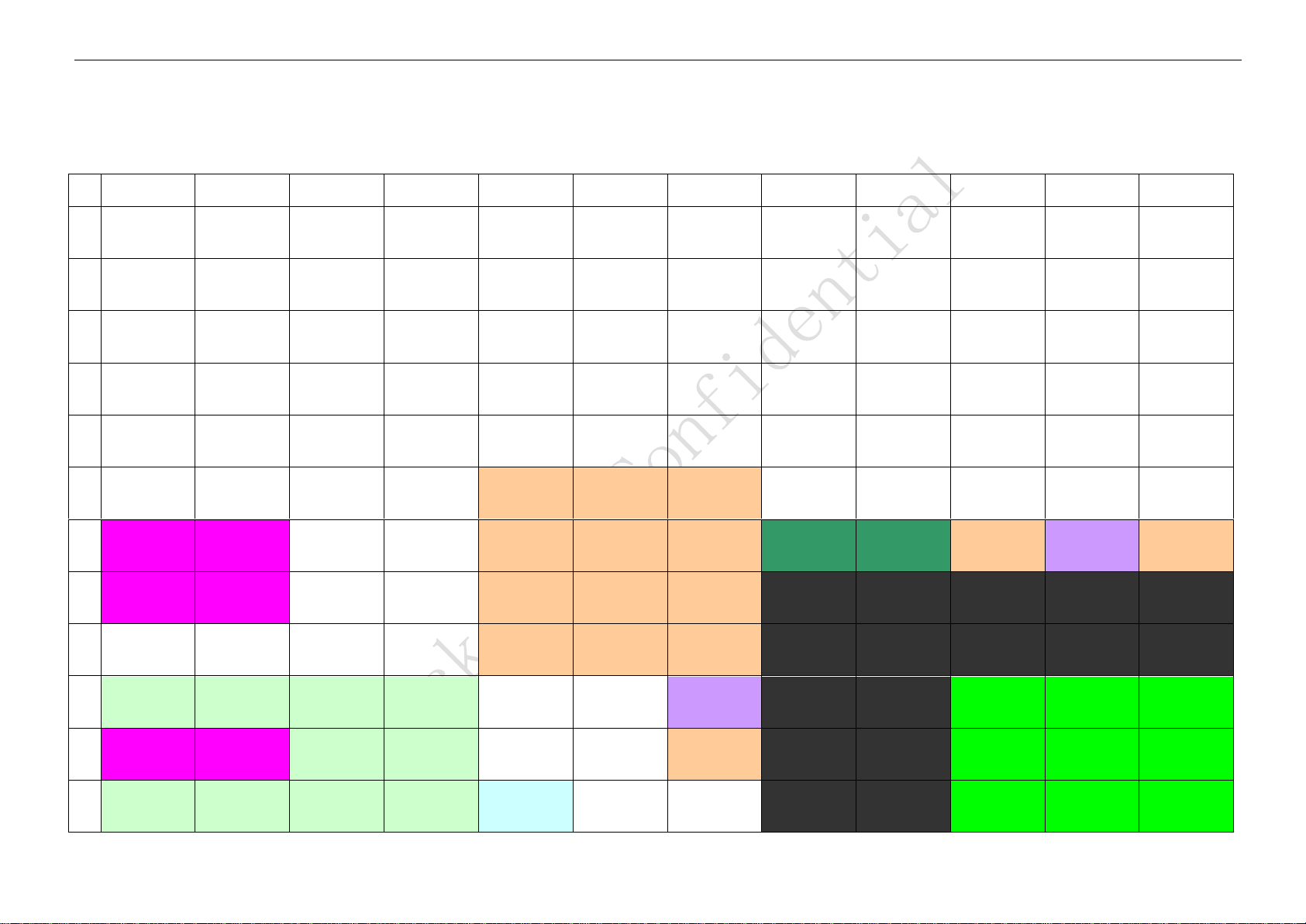
1.2 Block Diagram
The following diagram shows the basic block diagram for RK2918.
Rockchips Confidential 19
Page 20
RK2918 Datasheet Rev 1.0
RK2918
32KB ICache
ETM NEON
Cortex-A8
32KB DCache
512KB L2 Cache
TrustZone
LCD Controller
(1920x1080 output
24 bits panel
4-layer window
Scale up/Down)
EPD driver I/F
Camera I/F
(8bits CCIR / 8bits
Sensor)
Image Interface
2D Graphics Engine
1080p Video encoder
(H.264)
Image pre processor
3D Graphics Engine
1080p Video decoder
(H263/H264/MPEG2
/MPEG4/VC-1/VP8/
RMVB/AVS)
JPEG Encoder
Image post processor
JPEG Decoder
Multi-Media Processor
SDR/DDR/LBA Nand
Flash
(24bit ECC)
LPDDR
(200MHz, 32bits)
External Memory Interface
DDRII
(400MHz,
32bits/16bits)
SD2.0 / HS-MMC4.2
(8bits)
Inand /eMMC I/F
Nor Flash /Async
SRAM
USB OTG 2.0
SDIO
UARTx4
I2S/PCM
(M/S) (8ch )
I2C x4
SPI(M/S) x2
GPIO
SPDIF (1ch)
USB HOST 2.0
USB HOST 1.1
Modem I/F
MAC (MII/RMII)
I2S/PCM
(M/S) (2ch)
TS I/F
Connectivity
DMACx2 (13ch)
Interrupt Controller
PMU
PWMx3
WatchDog
Timerx4
Clock & Reset
System register
RTC
SAR-ADC
PLL x 4
System Peripheral
SRAM (16KB)
(security/non-security)
ROM (10KB)
eFuse
(128 x 8bits )
Memory
Rockchips Confidential 20
Fig. 1-1 RK2918 Block Diagram
Page 21
RK2918 Datasheet Rev 1.0
1 2 3 4 5 6 7 8 9
10
11
12
A
GPIO6_A[0]
GPIO6_B[7]
GPIO1_C[0]/
UART0_CTS_N/
SDMMC1_DETECT_
N
GPIO3_A[5]/
I2S1_LRCK_TX
GPIO3_A[4]/
I2S1_SDO
GPIO5_D[6]/
SDMMC1_PWR_EN
GPIO5_D[5]/
SDMMC0_PWR_EN
GPIO2_B[2]/
UART3_SIN
GPIO1_A[5]/
EMMC_PWR_EN/
PWM3
GPIO1_A[4]/EMMC
_WRITE_PRT/SPI0_
CSN1
GPIO6_C[2]
GPIO1_A[6]/
I2C1_SDA
B
GPIO6_B[6]
GPIO6_B[5]
GPIO6_A[1]
GPIO2_A[7]/
UART2_RTS_N
GPIO3_A[3]/
I2S1_SDI
GPIO3_A[1]/
I2S1_SCLK
GPIO5_D[2]/
PWM1/
UART1_SIR_IN
GPIO5_D[3]/
I2C2_SDA
GPIO2_A[3]/
SDMMC0_WRITE_P
RT/
PWM2/
UART1_SIR_OUT
GPIO2_A[2]/
SDMMC0_DETECT_
N
GPIO4_A[6]/
OTG1_DRV_VBUS
GPIO1_A[7]/
I2C1_SCL
C
GPIO6_A[5]
GPIO6_B[4]
GPIO6_A[2]
GPIO1_C[1]/
UART0_RTS_N/
SDMMC1_WRITE_P
RT
GPIO2_A[6]/
UART2_CTS_N
GPIO3_A[2]/
I2S1_LRCK_RX
GPIO2_A[4]/
UART1_SIN
GPIO1_B[5]/
PWM0
GPIO2_B[6]/
I2C0_SDA
GPIO4_D[4]
GPIO6_C[6]
GPIO6_C[0]
D
GPIO6_A[6]
GPIO6_A[7]
GPIO6_B[3]
GPIO6_A[3]
GPIO1_B[7]/
UART0_SOUT
GPIO2_B[4]/
UART3_CTS_N/
I2C3_SDA
GPIO3_A[0]/
I2S1_CLK
GPIO1_B[6]/
UART0_SIN
GPIO5_D[4]/
I2C2_SCL
GPIO2_B[7]/
I2C0_SCL
GPIO0_A[7]/
MII_MDCLK
GPIO4_D[0]
E
GPIO6_B[0]
GPIO5_A[0]
GPIO6_B[2]
GPIO5_A[2]
GPIO6_A[4]
GPIO2_B[0]/
UART2_SIN
GPIO2_B[5]/
UART3_RTS_N/
I2C3_SCL
GPIO2_B[1]/
UART2_SOUT
GPIO2_A[5]/
UART1_SOUT
GPIO6_C[5]
GPIO4_D[1]
GPIO6_C[1]
F
GPIO6_B[1]
GPIO0_A[1]
GPIO5_A[1]
GPIO0_A[0]
AVDD_DPLL
AHVDD_APLL
AHVSS_APLL
GPIO2_B[3]/
UART3_SOUT
GPIO4_D[3]
GPIO4_D[2]
GPIO4_D[5]
GPIO5_D[7]
G
XOUT24M
XIN24M
GPIO0_A[2]
GPIO0_A[4]
DVDD_APLL
AVSS_DPLL
DVSS_APLL
VDDIO_AP1
VDDIO_AP0
VDDCORE
VDDIO6
VDDCORE
H
XOUT27M
XIN27M
GPIO0_A[3]
GPIO4_A[3]
DVDD_DPLL
DVSS_DPLL
DVSS_CGPLL
NP
NP
NP
NP
NP
J
GPIO4_A[0]
GPIO4_A[1]
GPIO4_A[2]
GPIO4_A[4]
AVDD_CGPLL
DVDD_CGPLL
AVSS_CGPLL
NP
NP
NP
NP
NP
K
DQ[3]
DQ[2]
DQ[1]
DQ[0]
TRST_N
NPOR
VDDIO0
NP
NP
GND
GND
GND
L
DQS[0]
DQS_b[0]
DQ[5]
DQ[4]
TCK
TDI
VDDCORE
NP
NP
GND
GND
GND
M
DQ[7]
DQ[6]
DQ[17]
DM[0]
VSSIO_DDR0
TMS
TDO
NP
NP
GND
GND
GND
Chapter 2 Package Description
2.1 Ball Map
Rockchips Confidential 21
Page 22

RK2918 Datasheet Rev 1.0
13
14
15
16
17
18
19
20
21
22
23
24
GPIO2_C[5]/
SPI1_CSN0
GPIO3_C[2]/
SMC_ADDR[13]/
HOST_DATA[13]
GPIO3_D[1]/
SMC_ADDR[19]/
HOST_ADDR1
GPIO3_C[4]/
SMC_ADDR[11]/
HOST_DATA[11]
GPIO5_B[3]/
HSADC_DATA6
GPIO4_C[5]/
RMII_CRS_DVALID
/
MII_RXD_VALID
GPIO5_A[7]/
HSADC_DATA2
GPIO4_C[0]/
RMII_CLKOUT/
RMII_CLKIN
GPIO2_D[2]/
I2S0_LRCK_RX/
MII_TX_ERR
GPIO4_C[1]/
RMII_TX_EN/
MII_TX_EN
GPIO2_D[5]/
I2S0_SDO1/
MII_RXD3
GPIO2_D[6]/
I2S0_SDO2/
MII_TXD2
A
GPIO3_A[7]/
SMC_ADDR[15]/
HOST_DATA[15]
GPIO3_C[6]/
SMC_ADDR[16]/
HOST_DATA[16]
GPIO3_C[5]/
SMC_ADDR[12]/
HOST_DATA[12]
GPIO2_C[6]/
SPI1_TXD
GPIO5_B[2]/
HSADC_DATA5
GPIO5_A[3]/
MII_TX_CLKIN
GPIO5_B[5]/
HSADC_DATA8/
TS_VALID
GPIO5_A[5]/
HSADC_DATA0
GPIO4_D[7]/
I2S0_LRCK_TX1
GPIO2_D[3]/
I2S0_SDI/
MII_COL
GPIO4_C[6]/
RMII_RXD1/
MII_RXD1
GPIO1_D[4]/
SDMMC0_DATA2
B
GPIO5_B[6]/
HSADC_DATA9/
TS_FAIL
GPIO2_C[7]/
SPI1_RXD
GPIO4_A[7]/
SPDIF_TX
GPIO5_A[4]/
TS_SYNC
GPIO5_B[4]/
HSADC_DATA7
GPIO4_C[4]/
RMII_RX_ERR/
MII_RX_ERR
GPIO4_C[2]/
RMII_TXD1/
MII_TXD1
GPIO5_B[1]/
HSADC_DATA4
GPIO2_D[4]/
I2S0_SDO0/
MII_RXD2
GPIO2_A[0]/
SDMMC0_DATA6
GPIO1_D[6]/
SDMMC0_DATA4
GPIO2_D[7]/
I2S0_SDO3/
MII_TXD3
C
GPIO6_C[3]
GPIO2_C[0]/
SPI0_CLK
GPIO2_C[3]/
SPI0_RXD
GPIO3_C[7]/
SMC_ADDR[17]/
HOST_DATA[17]
GPIO3_D[2]/
HOST_CSN
GPIO0_A[6]/
MII_MD
GPIO3_D[4]/
HOST_WRN
GPIO1_D[2]/
SDMMC0_DATA0
GPIO4_C[3]/
RMII_TXD0/
MII_TXD0
GPIO1_D[0]/
SDMMC0_CLKOUT
GPIO3_B[7]/
EMMC_DATA5
GPIO1_C[2]/
SDMMC1_CMD
D
GPIO6_C[7]
GPIO2_C[1]/
SPI0_CSN0
GPIO2_C[2]/
SPI0_TXD
GPIO3_C[3]/
SMC_ADDR[10]/
HOST_DATA[10]
GPIO3_D[7]/
SMC_ADDR[9]/
HOST_DATA[9]
GPIO3_D[3]/
HOST_RDN
GPIO4_C[7]/
RMII_RXD0/
MII_RXD0
GPIO1_D[7]/
SDMMC0_DATA5
GPIO5_B[0]/
HSADC_DATA3
GPIO3_B[0]/
EMMC_CLKOUT
GPIO2_A[1]/
SDMMC0_DATA7
GPIO2_D[0]/
I2S0_CLK/
MII_RX_CLKIN
E
GPIO6_C[4]
GPIO3_D[0]/
SMC_ADDR[18]/
HOST_ADDR0
GPIO1_A[3]/
EMMC_DETECT_N/
SPI1_CSN1
GPIO2_C[4]/
SPI1_CLK
GPIO3_A[6]/
SMC_ADDR[14]/
HOST_DATA[14]
GPIO5_A[6]/
HSADC_DATA1
GPIO5_B[7]/
HSADC_CLKOUT
GPIO4_D[6]/
I2S0_LRCK_TX0
GPIO3_C[0]/
EMMC_DATA6
GPIO3_B[2]/
EMMC_DATA0
GPIO3_B[4]/
EMMC_DATA2
GPIO3_B[5]/
EMMC_DATA3
F
VDDIO5
VDDCORE
VDDIO4
VDDCORE
GPIO4_A[5]/
OTG0_DRV_VBUS
VDDIO3
GPIO1_D[5]/
SDMMC0_DATA3
GPIO1_D[1]/
SDMMC0_CMD
GPIO3_C[1]/
EMMC_DATA7
GPIO1_D[3]/
SDMMC0_DATA1
GPIO3_B[6]/
EMMC_DATA4
GPIO1_C[7]/
SDMMC1_CLKOUT
G
NP
NP
NP
NP
NP
GPIO1_C[5]/
SDMMC1_DATA2
GPIO1_C[6]/
SDMMC1_DATA3
GPIO2_D[1]/
I2S0_SCLK/
MII_CRS
GPIO3_B[1]/
EMMC_CMD
GPIO1_C[3]/
SDMMC1_DATA0
GPIO1_C[4]/
SDMMC1_DATA1
GPIO3_B[3]/
EMMC_DATA1
H
NP
NP
NP
NP
NP
VDDCORE
GPIO0_D[6]/
FLASH_CSN5
GPIO1_A[0]/
FLASH_CSN7/
MDDR_TQ
GPIO0_A[5]/
FLASH_DQS
GPIO0_D[5]/
FLASH_CSN4
GPIO4_B[2]/
FLASH_DATA[10]
GPIO4_B[3]/
FLASH_DATA[11]
J
GND
GND
GND
NP
NP
VDDIO2
FLASH_WP
FLASH_WRN
GPIO4_B[6]/
FLASH_DATA[14]
GPIO0_D[3]/
FLASH_CSN2
GPIO0_D[4]/
FLASH_CSN3
GPIO0_D[2]/
FLASH_CSN1
K
GND
GND
GND
NP
NP
VDDCORE
FLASH_DATA[6]
GPIO4_B[0]/
FLASH_DATA[8]
FLASH_DATA[7]
FLASH_DATA[2]
FLASH_DATA[3]
GPIO0_D[7]/
FLASH_CSN6
L
GND
GND
GND
NP
NP
VDDIO_FLASH1
GPIO4_B[7]/
FLASH_DATA[15]
GPIO4_B[5]/
FLASH_DATA[13]
FLASH_CLE
GPIO4_B[1]/
FLASH_DATA[9]
FLASH_DATA[5]
FLASH_CSN0
M
Rockchips Confidential 22
Page 23

RK2918 Datasheet Rev 1.0
N
DQ[19]
DQ[18]
DM[2]
DQ[16]
VDDIO_DDR0
BTMODE
VDDCORE
NP
NP
GND
GND
GND
P
DQS[2]
DQS_B[2]
DQ[21]
DQ[20]
VSSIO_DDR1
VREF0
EWAKEUP_STOP
NP
NP
GND
GND
GND R DQ[23]
DQ[22]
BA[0]
ZQ_PIN
VDDIO_DDR1
LCDC_BYP
VDDCORE
NP
NP
GND
GND
GND T A[1]
A[0]
BA[1]
BA[2]
VSSIO_DDR2
ANALOG_TEST_
PIN
EWAKEUP_POW
ER
NP
NP
NP
NP
NP U A[2]
A[3]
NC0
NC1
VDDIO_DDR2
VREF1
VDDCORE
NP
NP
NP
NP
NP V A[6]
CS_B0
A[4]
A[5]
VSSIO_DDR3
RESET
TEST
GPIO6_D[2]
GPIO6_D[0]
VDDCORE
VDDIO_LCD0
VDDCORE
W
CS_B1
ODT0
CKE1
RET_EN
VDDIO_DDR3
VREF2
GPIO6_D[3]
GPIO6_D[1]
NC6
LCDC_DATA[0]/
EBC_SDDO[0]
LCDC_HSYNC/
EBC_SDLE
LCDC_DATA[23]/
EBC_GDRL
Y
CK
CK_B
CKE0
DLL_TEST_PIN[1]
VSSIO_DDR4
VDDIO_DDR4
VSSIO_DDR5
VDDIO_DDR5
VSSIO_DDR6
VDDIO_DDR6
LCDC_DATA[18]/
EBC_GDPWR2
LCDC_DATA[9]/
EBC_SDCE1
AA
WE_B
CAS_B
ODT1
NC3
DLL_TEST_PIN[0]
DQ[12]
DQ[13]
NC4
DQ[28]
DQ[27]
LCDC_DATA[20]/
EBC_SDSHR
LCDC_DCLK/
EBC_SDCLK
AB
A[10]
RAS_B
NC2
A[14]
DQ[9]
DQ[10]
DM[3]
NC5
DQ[26]
DQ[30]
LCDC_DATA[5]/
EBC_SDDO[5]
LCDC_DATA[3]/
EBC_SDDO[3]
AC
A[8]
A[13]
A[7]
DQ[8]
DM[1]
DQS_b[1]
DQ[14]
DQ[24]
DQS_B[3]
DQ[29]
LCDC_DATA[1]/
EBC_SDDO[1]
LCDC_DATA[2]/
EBC_SDDO[2]
AD
A[11]
A[15]
A[9]
A[12]
DQ[11]
DQS[1]
DQ[15]
DQ[25]
DQS[3]
DQ[31]
LCDC_DATA[4]/
EBC_SDDO[4]
LCDC_DATA[6]/
EBC_SDDO[6]
1 2 3 4 5 6 7 8 9 10
11
12
Rockchips Confidential 23
Page 24

RK2918 Datasheet Rev 1.0
GND
GND
GND
NP
NP
VDDCORE
FLASH_DATA[1]
FLASH_RDY
FLASH_RDN
GPIO4_B[4]/
FLASH_DATA[12]
FLASH_DATA[0]
FLASH_DATA[4]
N
GND
GND
GND
NP
NP
VDDIO_FLASH0
FLASH_ALE
VDDCORE_EFUS
E
VDDIO_RTC
RTCINT_OUT
XOUT32K
XIN32K
P
GND
GND
GND
NP
NP
VDDCORE
GPIO3_D[6]/
SMC_ADDR[8]/
HOST_DATA[8]
EFUSE_VQPS
VSSIO_UHOST
VDDIO_UHOST
USBHOST_DN
USBHOST_DP
R
NP
NP
NP
NP
NP
VDDIO1
VDDIO_EFUSE
OTG1_ID
OTG1_VSSA
OTG1_VDD25
OTG1_DM
OTG1_DP
T
NP
NP
NP
NP
NP
VDDCORE_RTC
OTG1_DVDD
OTG1_VSSAC
OTG1_DVSS
OTG1_VBUS
OTG1_VDD33
OTG1_RKELVIN
U
VDDIO_LCD1
VDDCORE
VDDIO_VIP
VDDCORE
VDDIO_SMC0
VDDIO_SMC1
OTG0_DVDD
OTG0_ID
OTG0_VSSA
OTG0_VDD25
OTG0_DM
OTG0_DP
V
LCDC_DATA[22]/
EBC_GDSP
LCDC_DATA[21]/
EBC_GDOE
VIP_DATAIN[4]
GPIO1_B[4]/
VIP_CLKOUT
GPIO1_A[1]/
SMC_CSN0
GPIO5_C[4]/
EBC_SDDO[4]/
SMC_DATA[4]
GPIO5_D[1]/
EBC_SDCLK/
SMC_ADDR[6]/
HOST_DATA[6]
OTG0_VSSAC
OTG0_DVSS
OTG0_VBUS
OTG0_VDD33
OTG0_RKELVIN
W
LCDC_DATA[19]/
EBC_VCOM
LCDC_DEN/
EBC_GDCLK
VIP_DATAIN[11]
VIP_DATAIN[7]
GPIO0_B[5]/
EBC_VCOM/
SMC_BLSN0
GPIO5_C[0]/
EBC_SDDO[0]/
SMC_DATA[0]
GPIO5_D[0]/
EBC_SDLE/
SMC_ADDR[5]/
HOST_DATA[5]
GPIO0_C[4]/
EBC_GDPWR2/
SMC_DATA[12]
GPIO1_A[2]/
SMC_CSN1
GPIO3_D[5]/
SMC_ADDR[7]/
HOST_DATA[7]
SARADC_AIN[1]
SARADC_AIN[2]
Y
LCDC_DATA[10]/
EBC_SDCE2
LCDC_DATA[14]/
EBC_BORDER0
VIP_DATAIN[10]
GPIO1_B[0]/
VIP_DATAIN[0]
GPIO1_B[1]/
VIP_DATAIN[1]
GPIO5_C[1]/
EBC_SDDO[1]/
SMC_DATA[1]
GPIO0_B[6]/
EBC_SDSHR/
SMC_BLSN1/
HOST_INT
GPIO5_C[5]/
EBC_SDDO[5]/
SMC_DATA[5]
GPIO0_B[1]/
EBC_SDCE1/
SMC_ADDR[1]/
HOST_DATA[1]
GPIO0_C[5]/
EBC_SDCE3/
SMC_DATA[13]
SARADC_AIN[0]
SARADC_AIN[3]
AA
LCDC_VSYNC/
EBC_SDOE
LCDC_DATA[11]/
EBC_SDCE3
LCDC_DATA[15]/
EBC_BORDER1
VIP_DATAIN[5]
VIP_DATAIN[8]
VIP_VSYNC
GPIO0_C[2]/
EBC_GDPWR0/
SMC_DATA[10]
GPIO5_C[6]/EBC
_SDDO[6]/SMC_
DATA[6]
GPIO0_D[0]/
EBC_SDOE/
SMC_ADVN
GPIO0_B[7]/
EBC_GDOE/
SMC_OEN
GPIO0_C[3]/
EBC_GDPWR1/
SMC_DATA[11]
VDDA_SARADC
AB
LCDC_DATA[7]/
EBC_SDDO[7]
LCDC_DATA[12]/
EBC_SDCE4
LCDC_DATA[16]/
EBC_GDPWR0
VIP_DATAIN[6]
VIP_HREF
GPIO1_B[3]/
VIP_DATAIN[3]
GPIO5_C[2]/
EBC_SDDO[2]/
SMC_DATA[2]
GPIO5_C[7]/
EBC_SDDO[7]/
SMC_DATA[7]
GPIO0_D[1]/
EBC_GDCLK/
SMC_ADDR[4]/
HOST_DATA[4]
GPIO0_B[3]/
EBC_BORDER0/
SMC_ADDR[3]/
HOST_DATA[3]
GPIO0_C[0]/
EBC_GDSP/
SMC_DATA[8]
GPIO0_C[6]/
EBC_SDCE4/
SMC_DATA[14]
AC
LCDC_DATA[8]/
EBC_SDCE0
LCDC_DATA[13]/
EBC_SDCE5
LCDC_DATA[17]/
EBC_GDPWR1
VIP_DATAIN[9]
VIP_CLKIN
GPIO1_B[2]/
VIP_DATAIN[2]
GPIO5_C[3]/
EBC_SDDO[3]/
SMC_DATA[3]
GPIO0_B[0]/EBC
_SDCE0/SMC_A
DDR[0]/HOST_D
ATA[0]
GPIO0_B[2]/
EBC_SDCE2/
SMC_ADDR[2]/
HOST_DATA[2]
GPIO0_B[4]/
EBC_BORDER1/
SMC_WEN
GPIO0_C[1]/
EBC_GDRL/
SMC_DATA[9]
GPIO0_C[7]/
EBC_SDCE5/
SMC_DATA[15]
AD
13
14
15
16
17
18
19
20
21
22
23
24
Fig. 2-1 RK2908 Ball Mapping Diagram
Rockchips Confidential 24
Page 25

RK2918 Datasheet Rev 1.0
Ball #
Pin Name
Ball #
Pin Name
A1
GPIO6_A[0]
B1
GPIO6_B[6]
A2
GPIO6_B[7]
B2
GPIO6_B[5]
A3
GPIO1_C[0]/UART0_CTS_N/SDIO_DETECT_N
B3
GPIO6_A[1]
A4
GPIO3_A[5]/I2S1_LRCK_TX
B4
GPIO2_A[7]/UART2_RTS_N
A5
GPIO3_A[4]/I2S1_SDO
B5
GPIO3_A[3]/I2S1_SDI
A6
GPIO5_D[6]/SDIO_PWR_EN
B6
GPIO3_A[1]/I2S1_SCLK
A7
GPIO5_D[5]/SDMMC_PWR_EN
B7
GPIO5_D[2]/PWM1/UART1_SIR_IN
A8
GPIO2_B[2]/UART3_SIN
B8
GPIO5_D[3]/I2C2_SDA
A9
GPIO1_A[5]/EMMC_PWR_EN/PWM3
B9
GPIO2_A[3]/SDMMC_WRITE_PRT/PWM2/UART1_SIR_OUT
A10
GPIO1_A[4]/EMMC_WRITE_PRT/SPI0_CSN1
B10
GPIO2_A[2]/SDMMC_DETECT_N
A11
GPIO6_C[2]
B11
GPIO4_A[6]/OTG1_DRV_VBUS
A12
GPIO1_A[6]/I2C1_SDA
B12
GPIO1_A[7]/I2C1_SCL
A13
GPIO2_C[5]/SPI1_CSN0
B13
GPIO3_A[7]/SMC_ADDR[15]/HOST_DATA[15]
A14
GPIO3_C[2]/SMC_ADDR[13]/HOST_DATA[13]
B14
GPIO3_C[6]/SMC_ADDR[16]/HOST_DATA[16]
A15
GPIO3_D[1]/SMC_ADDR[19]/HOST_ADDR1
B15
GPIO3_C[5]/SMC_ADDR[12]/HOST_DATA[12]
A16
GPIO3_C[4]/SMC_ADDR[11]/HOST_DATA[11]
B16
GPIO2_C[6]/SPI1_TXD
A17
GPIO5_B[3]/HSADC_DATA6
B17
GPIO5_B[2]/HSADC_DATA5
A18
GPIO4_C[5]/RMII_CRS_DVALID/MII_RXD_VALID
B18
GPIO5_A[3]/MII_TX_CLKIN
A19
GPIO5_A[7]/HSADC_DATA2
B19
GPIO5_B[5]/HSADC_DATA8/TS_VALID
A20
GPIO2_D[2]/I2S0_LRCK_RX/MII_TX_ERR
B20
GPIO5_A[5]/HSADC_DATA0
A21
GPIO2_D[5]/I2S0_SDO1/MII_RXD3
B21
GPIO4_D[7]/I2S0_LRCK_TX1
A22
GPIO2_D[6]/I2S0_SDO2/MII_TXD2
B22
GPIO2_D[3]/I2S0_SDI/MII_COL
A23
GPIO4_C[0]/RMII_CLKOUT/RMII_CLKIN
B23
GPIO4_C[6]/RMII_RXD1/MII_RXD1
A24
GPIO4_C[1]/RMII_TX_EN/MII_TX_EN
B24
GPIO1_D[4]/SDMMC_DATA2
C1
GPIO6_A[5]
D1
GPIO6_A[6]
C2
GPIO6_B[4]
D2
GPIO6_A[7]
C3
GPIO6_A[2]
D3
GPIO6_B[3]
C4
GPIO1_C[1]/UART0_RTS_N/SDIO_WRITE_PRT
D4
GPIO6_A[3]
C5
GPIO2_A[6]/UART2_CTS_N
D5
GPIO1_B[7]/UART0_SOUT
C6
GPIO3_A[2]/I2S1_LRCK_RX
D6
GPIO2_B[4]/UART3_CTS_N/I2C3_SDA
C7
GPIO2_A[4]/UART1_SIN
D7
GPIO3_A[0]/I2S1_CLK
C8
GPIO1_B[5]/PWM0
D8
GPIO1_B[6]/UART0_SIN
C9
GPIO2_B[6]/I2C0_SDA
D9
GPIO5_D[4]/I2C2_SCL
C10
GPIO4_D[4]
D10
GPIO2_B[7]/I2C0_SCL
C11
GPIO6_C[6]
D11
GPIO0_A[7]/MII_MDCLK
C12
GPIO6_C[0]
D12
GPIO4_D[0]
C13
GPIO5_B[6]/HSADC_DATA9/TS_FAIL
D13
GPIO6_C[3]
C14
GPIO2_C[7]/SPI1_RXD
D14
GPIO2_C[0]/SPI0_CLK
C15
GPIO4_A[7]/SPDIF_TX
D15
GPIO2_C[3]/SPI0_RXD
C16
GPIO5_A[4]/TS_SYNC
D16
GPIO3_C[7]/SMC_ADDR[17]/HOST_DATA[17]
C17
GPIO5_B[4]/HSADC_DATA7
D17
GPIO3_D[2]/HOST_CSN
C18
GPIO4_C[4]/RMII_RX_ERR/MII_RX_ERR
D18
GPIO0_A[6]/MII_MD
2.2 Pin Number Order
Table 2-1 RK2908 Pin Number Order Information
Rockchips Confidential 25
Page 26

RK2918 Datasheet Rev 1.0
C19
GPIO4_C[2]/RMII_TXD1/MII_TXD1
D19
GPIO3_D[4]/HOST_WRN
C20
GPIO5_B[1]/HSADC_DATA4
D20
GPIO1_D[2]/SDMMC_DATA0
C21
GPIO2_D[4]/I2S0_SDO0/MII_RXD2
D21
GPIO4_C[3]/RMII_TXD0/MII_TXD0
C22
GPIO2_A[0]/SDMMC_DATA6
D22
GPIO1_D[0]/SDMMC_CLKOUT
C23
GPIO1_D[6]/SDMMC_DATA4
D23
GPIO3_B[7]/EMMC_DATA5
C24
GPIO2_D[7]/I2S0_SDO3/MII_TXD3
D24
GPIO1_C[2]/SDIO_CMD
E1
GPIO6_B[0]
F1
GPIO6_B[1]
E2
GPIO5_A[0]
F2
GPIO0_A[1]
E3
GPIO6_B[2]
F3
GPIO5_A[1]
E4
GPIO5_A[2]
F4
GPIO0_A[0]
E5
GPIO6_A[4]
F5
AVDD_DPLL
E6
GPIO2_B[0]/UART2_SIN
F6
AHVDD_APLL
E7
GPIO2_B[5]/UART3_RTS_N/I2C3_SCL
F7
AHVSS_APLL
E8
GPIO2_B[1]/UART2_SOUT
F8
GPIO2_B[3]/UART3_SOUT
E9
GPIO2_A[5]/UART1_SOUT
F9
GPIO4_D[3]
E10
GPIO6_C[5]
F10
GPIO4_D[2]
E11
GPIO4_D[1]
F11
GPIO4_D[5]
E12
GPIO6_C[1]
F12
GPIO5_D[7]
E13
GPIO6_C[7]
F13
GPIO6_C[4]
E14
GPIO2_C[1]/SPI0_CSN0
F14
GPIO3_D[0]/SMC_ADDR[18]/HOST_ADDR0
E15
GPIO2_C[2]/SPI0_TXD
F15
GPIO1_A[3]/EMMC_DETECT_N/SPI1_CSN1
E16
GPIO3_C[3]/SMC_ADDR[10]/HOST_DATA[10]
F16
GPIO2_C[4]/SPI1_CLK
E17
GPIO3_D[7]/SMC_ADDR[9]/HOST_DATA[9]
F17
GPIO3_A[6]/SMC_ADDR[14]/HOST_DATA[14]
E18
GPIO3_D[3]/HOST_RDN
F18
GPIO5_A[6]/HSADC_DATA1
E19
GPIO4_C[7]/RMII_RXD0/MII_RXD0
F19
GPIO5_B[7]/HSADC_CLKOUT/GPS_CLK
E20
GPIO1_D[7]/SDMMC_DATA5
F20
GPIO4_D[6]/I2S0_LRCK_TX0
E21
GPIO5_B[0]/HSADC_DATA3
F21
GPIO3_C[0]/EMMC_DATA6
E22
GPIO3_B[0]/EMMC_CLKOUT
F22
GPIO3_B[2]/EMMC_DATA0
E23
GPIO2_A[1]/SDMMC_DATA7
F23
GPIO3_B[4]/EMMC_DATA2
E24
GPIO2_D[0]/I2S0_CLK/MII_RX_CLKIN
F24
GPIO3_B[5]/EMMC_DATA3
G1
XOUT24M
H1
XOUT27M
G2
XIN24M
H2
XIN27M
G3
GPIO0_A[2]
H3
GPIO0_A[3]
G4
GPIO0_A[4]
H4
GPIO4_A[3]
G5
DVDD_APLL
H5
DVDD_DPLL
G6
AVSS_DPLL
H6
DVSS_DPLL
G7
DVSS_APLL
H7
DVSS_CGPLL
G8
VDDIO_AP1
H18
GPIO1_C[5]/SDIO_DATA2
G9
VDDIO_AP0
H19
GPIO1_C[6]/SDIO_DATA3
G10
VDDCORE
H20
GPIO2_D[1]/I2S0_SCLK/MII_CRS
G11
VDDIO6
H21
GPIO3_B[1]/EMMC_CMD
G12
VDDCORE
H22
GPIO1_C[3]/SDIO_DATA0
G13
VDDIO5
H23
GPIO1_C[4]/SDIO_DATA1
G14
VDDCORE
H24
GPIO3_B[3]/EMMC_DATA1
G15
VDDIO4
K1
DQ[3]
G16
VDDCORE
K2
DQ[2]
Rockchips Confidential 26
Page 27

RK2918 Datasheet Rev 1.0
G17
GPIO4_A[5]/OTG0_DRV_VBUS
K3
DQ[1]
G18
VDDIO3
K4
DQ[0]
G19
GPIO1_D[5]/SDMMC_DATA3
K5
TRST_N
G20
GPIO1_D[1]/SDMMC_CMD
K6
NPOR
G21
GPIO3_C[1]/EMMC_DATA7
K7
VDDIO0
G22
GPIO1_D[3]/SDMMC_DATA1
K10
GND
G23
GPIO3_B[6]/EMMC_DATA4
K11
GND
G24
GPIO1_C[7]/SDIO_CLKOUT
K12
GND
J1
GPIO4_A[0]
K13
GND
J2
GPIO4_A[1]
K14
GND
J3
GPIO4_A[2]
K15
GND
J4
GPIO4_A[4]
K18
VDDIO2
J5
AVDD_CGPLL
K19
FLASH_WP
J6
DVDD_CGPLL
K20
FLASH_WRN
J7
AVSS_CGPLL
K21
GPIO4_B[6]/FLASH_DATA[14]
J18
VDDCORE
K22
GPIO0_D[3]/FLASH_CSN2
J19
GPIO0_D[6]/FLASH_CSN5
K23
GPIO0_D[4]/FLASH_CSN3
J20
GPIO1_A[0]/FLASH_CSN7/MDDR_TQ
K24
GPIO0_D[2]/FLASH_CSN1
J21
GPIO0_A[5]/FLASH_DQS
M1
DQ[7]
J22
GPIO0_D[5]/FLASH_CSN4
M2
DQ[6]
J23
GPIO4_B[2]/FLASH_DATA[10]
M3
DQ[17]
J24
GPIO4_B[3]/FLASH_DATA[11]
M4
DM[0]
L1
DQS[0]
M5
VSSIO_DDR0
L2
DQS_B[0]
M6
TMS
L3
DQ[5]
M7
TDO
L4
DQ[4]
M10
GND
L5
TCK
M11
GND
L6
TDI
M12
GND
L7
VDDCORE
M13
GND
L10
GND
M14
GND
L11
GND
M15
GND
L12
GND
M18
VDDIO_FLASH1
L13
GND
M19
GPIO4_B[7]/FLASH_DATA[15]
L14
GND
M20
GPIO4_B[5]/FLASH_DATA[13]
L15
GND
M21
FLASH_CLE
L18
VDDCORE
M22
GPIO4_B[1]/FLASH_DATA[9]
L19
FLASH_DATA[6]
M23
FLASH_DATA[5]
L20
GPIO4_B[0]/FLASH_DATA[8]
M24
FLASH_CSN0
L21
FLASH_DATA[7]
P1
DQS[2]
L22
FLASH_DATA[2]
P2
DQS_B[2]
L23
FLASH_DATA[3]
P3
DQ[21]
L24
GPIO0_D[7]/FLASH_CSN6
P4
DQ[20]
N1
DQ[19]
P5
VSSIO_DDR1
N2
DQ[18]
P6
VREF0
N3
DM[2]
P7
EWAKEUP_STOP
N4
DQ[16]
P10
GND
Rockchips Confidential 27
Page 28

RK2918 Datasheet Rev 1.0
N5
VDDIO_DDR0
P11
GND
N6
BTMODE
P12
GND
N7
VDDCORE
P13
GND
N10
GND
P14
GND
N11
GND
P15
GND
N12
GND
P18
VDDIO_FLASH0
N13
GND
P19
FLASH_ALE
N14
GND
P20
VDDCORE_EFUSE
N15
GND
P21
VDDIO_RTC
N18
VDDCORE
P22
RTCINT_OUT
N19
FLASH_DATA[1]
P23
XOUT32K
N20
FLASH_RDY
P24
XIN32K
N21
FLASH_RDN
T1
A[1]
N22
GPIO4_B[4]/FLASH_DATA[12]
T2
A[0]
N23
FLASH_DATA[0]
T3
BA[1]
N24
FLASH_DATA[4]
T4
BA[2]
R1
DQ[23]
T5
VSSIO_DDR2
R2
DQ[22]
T6
ANALOG_TEST_PIN
R3
BA[0]
T7
EWAKEUP_POWER
R4
ZQ_PIN
T18
VDDIO1
R5
VDDIO_DDR1
T19
VDDIO_EFUSE
R6
LCDC_BYP
T20
OTG1_ID
R7
VDDCORE
T21
OTG1_VSSA
R10
GND
T22
OTG1_VDD25
R11
GND
T23
OTG1_DM
R12
GND
T24
OTG1_DP
R13
GND
V1
A[6]
R14
GND
V2
CS_B0
R15
GND
V3
A[4]
R18
VDDCORE
V4
A[5]
R19
GPIO3_D[6]/SMC_ADDR[8]/HOST_DATA[8]
V5
VSSIO_DDR3
R20
EFUSE_VQPS
V6
RESET
R21
VSSIO_UHOST
V7
TEST
R22
VDDIO_UHOST
V8
GPIO6_D[2]
R23
USBHOST_DN
V9
GPIO6_D[0]
R24
USBHOST_DP
V10
VDDCORE
U1
A[2]
V11
VDDIO_LCD0
U2
A[3]
V12
VDDCORE
U3
NC0
V13
VDDIO_LCD1
U4
NC1
V14
VDDCORE
U5
VDDIO_DDR2
V15
VDDIO_VIP
U6
VREF1
V16
VDDCORE
U7
VDDCORE
V17
VDDIO_SMC0
U18
VDDCORE_RTC
V18
VDDIO_SMC1
U19
OTG1_DVDD
V19
OTG0_DVDD
U20
OTG1_VSSAC
V20
OTG0_ID
Rockchips Confidential 28
Page 29

RK2918 Datasheet Rev 1.0
U21
OTG1_DVSS
V21
OTG0_VSSA
U22
OTG1_VBUS
V22
OTG0_VDD25
U23
OTG1_VDD33
V23
OTG0_DM
U24
OTG1_RKELVIN
V24
OTG0_DP
W1
CS_B1
Y1
CK
W2
ODT0
Y2
CK_B
W3
CKE1
Y3
CKE0
W4
RET_EN
Y4
DLL_TEST_PIN[1]
W5
VDDIO_DDR3
Y5
VSSIO_DDR4
W6
VREF2
Y6
VDDIO_DDR4
W7
GPIO6_D[3]
Y7
VSSIO_DDR5
W8
GPIO6_D[1]
Y8
VDDIO_DDR5
W9
NC6
Y9
VSSIO_DDR6
W10
LCDC_DATA[0]/EBC_SDDO[0]
Y10
VDDIO_DDR6
W11
LCDC_HSYNC/EBC_SDLE
Y11
LCDC_DATA[18]/EBC_GDPWR2
W12
LCDC_DATA[23]/EBC_GDRL
Y12
LCDC_DATA[9]/EBC_SDCE1
W13
LCDC_DATA[22]/EBC_GDSP
Y13
LCDC_DATA[19]/EBC_VCOM
W14
LCDC_DATA[21]/EBC_GDOE
Y14
LCDC_DEN/EBC_GDCLK
W15
VIP_DATAIN[4]
Y15
VIP_DATAIN[11]
W16
GPIO1_B[4]/VIP_CLKOUT
Y16
VIP_DATAIN[7]
W17
GPIO1_A[1]/SMC_CSN0
Y17
GPIO0_B[5]/EBC_VCOM/SMC_BLSN0
W18
GPIO5_C[4]/EBC_SDDO[4]/SMC_DATA[4]
Y18
GPIO5_C[0]/EBC_SDDO[0]/SMC_DATA[0]
W19
GPIO5_D[1]/EBC_SDCLK/SMC_ADDR[6]/HOST_DATA[6]
Y19
GPIO5_D[0]/EBC_SDLE/SMC_ADDR[5]/HOST_DATA[5]
W20
OTG0_VSSAC
Y20
GPIO0_C[4]/EBC_GDPWR2/SMC_DATA[12]
W21
OTG0_DVSS
Y21
GPIO1_A[2]/SMC_CSN1
W22
OTG0_VBUS
Y22
GPIO3_D[5]/SMC_ADDR[7]/HOST_DATA[7]
W23
OTG0_VDD33
Y23
SARADC_AIN[1]
W24
OTG0_RKELVIN
Y24
SARADC_AIN[2]
AA1
WE_B
AB1
A[10]
AA2
CAS_B
AB2
RAS_B
AA3
ODT1
AB3
NC2
AA4
NC3
AB4
A[14]
AA5
DLL_TEST_PIN[0]
AB5
DQ[9]
AA6
DQ[12]
AB6
DQ[10]
AA7
DQ[13]
AB7
DM[3]
AA8
NC4
AB8
NC5
AA9
DQ[28]
AB9
DQ[26]
AA10
DQ[27]
AB10
DQ[30]
AA11
LCDC_DATA[20]/EBC_SDSHR
AB11
LCDC_DATA[5]/EBC_SDDO[5]
AA12
LCDC_DCLK/EBC_SDCLK
AB12
LCDC_DATA[3]/EBC_SDDO[3]
AA13
LCDC_DATA[10]/EBC_SDCE2
AB13
LCDC_VSYNC/EBC_SDOE
AA14
LCDC_DATA[14]/EBC_BORDER0
AB14
LCDC_DATA[11]/EBC_SDCE3
AA15
VIP_DATAIN[10]
AB15
LCDC_DATA[15]/EBC_BORDER1
AA16
GPIO1_B[0]/VIP_DATAIN[0]
AB16
VIP_DATAIN[5]
AA17
GPIO1_B[1]/VIP_DATAIN[1]
AB17
VIP_DATAIN[8]
AA18
GPIO5_C[1]/EBC_SDDO[1]/SMC_DATA[1]
AB18
VIP_VSYNC
Rockchips Confidential 29
Page 30

RK2918 Datasheet Rev 1.0
AA19
GPIO0_B[6]/EBC_SDSHR/SMC_BLSN1/HOST_INT
AB19
GPIO0_C[2]/EBC_GDPWR0/SMC_DATA[10]
AA20
GPIO5_C[5]/EBC_SDDO[5]/SMC_DATA[5]
AB20
GPIO5_C[6]/EBC_SDDO[6]/SMC_DATA[6]
AA21
GPIO0_B[1]/EBC_SDCE1/SMC_ADDR[1]/HOST_DATA[1]
AB21
GPIO0_D[0]/EBC_SDOE/SMC_ADVN
AA22
GPIO0_C[5]/EBC_SDCE3/SMC_DATA[13]
AB22
GPIO0_B[7]/EBC_GDOE/SMC_OEN
AA23
SARADC_AIN[0]
AB23
GPIO0_C[3]/EBC_GDPWR1/SMC_DATA[11]
AA24
SARADC_AIN[3]
AB24
VDDA_SARADC
AC1
A[8]
AD1
A[11]
AC2
A[13]
AD2
A[15]
AC3
A[7]
AD3
A[9]
AC4
DQ[8]
AD4
A[12]
AC5
DM[1]
AD5
DQ[11]
AC6
DQS_B[1]
AD6
DQS[1]
AC7
DQ[14]
AD7
DQ[15]
AC8
DQ[24]
AD8
DQ[25]
AC9
DQS_B[3]
AD9
DQS[3]
AC10
DQ[29]
AD10
DQ[31]
AC11
LCDC_DATA[1]/EBC_SDDO[1]
AD11
LCDC_DATA[4]/EBC_SDDO[4]
AC12
LCDC_DATA[2]/EBC_SDDO[2]
AD12
LCDC_DATA[6]/EBC_SDDO[6]
AC13
LCDC_DATA[7]/EBC_SDDO[7]
AD13
LCDC_DATA[8]/EBC_SDCE0
AC14
LCDC_DATA[12]/EBC_SDCE4
AD14
LCDC_DATA[13]/EBC_SDCE5
AC15
LCDC_DATA[16]/EBC_GDPWR0
AD15
LCDC_DATA[17]/EBC_GDPWR1
AC16
VIP_DATAIN[6]
AD16
VIP_DATAIN[9]
AC17
VIP_HREF
AD17
VIP_CLKIN
AC18
GPIO1_B[3]/VIP_DATAIN[3]
AD18
GPIO1_B[2]/VIP_DATAIN[2]
AC19
GPIO5_C[2]/EBC_SDDO[2]/SMC_DATA[2]
AD19
GPIO5_C[3]/EBC_SDDO[3]/SMC_DATA[3]
AC20
GPIO5_C[7]/EBC_SDDO[7]/SMC_DATA[7]
AD20
GPIO0_B[0]/EBC_SDCE0/SMC_ADDR[0]/HOST_DATA[0]
AC21
GPIO0_D[1]/EBC_GDCLK/SMC_ADDR[4]/HOST_DATA[4]
AD21
GPIO0_B[2]/EBC_SDCE2/SMC_ADDR[2]/HOST_DATA[2]
AC22
GPIO0_B[3]/EBC_BORDER0/SMC_ADDR[3]/HOST_DATA[3]
AD22
GPIO0_B[4]/EBC_BORDER1/SMC_WEN
AC23
GPIO0_C[0]/EBC_GDSP/SMC_DATA[8]
AD23
GPIO0_C[1]/EBC_GDRL/SMC_DATA[9]
AC24
GPIO0_C[6]/EBC_SDCE4/SMC_DATA[14]
AD24
GPIO0_C[7]/EBC_SDCE5/SMC_DATA[15]
Group
Ball #
Min(V)
Typ(V)
Max(V)
Descriptions
GND
K10,K11,K12,K13,K14,K15,
L10,L11,L12,L13,L14,L15,
M10,M11,M12,M13,M14,M15,
N10,N11,N12,N13,N14,N15,
P10,P11,P12,P13,P14,P15,
R10,R11,R12,R13,R14,R15
0
Internal Core Ground
and digital IO Ground
VDDCORE
G10,G12,G14,G16,
L7,J18,N7,L18,
R7,N18,U7,R18,
V10,V12,V14,V16
1.08
1.2
1.32
Internal Core Power
(@ CPU frequency <= 1GHz)
2.3 RK2918 power/ground IO descriptions
Table 2-2 RK2918 Power/Ground IO informations
Rockchips Confidential 30
Page 31

RK2918 Datasheet Rev 1.0
VDDIO0
K7
3
3.3
3.6
Digital GPIO Power
VDDIO1
T18
3
3.3
3.6
Digital GPIO Power
VDDIO2
K18
3
3.3
3.6
VDDIO3
G18
3
3.3
3.6
VDDIO4
G15
3
3.3
3.6
VDDIO5
G13
3
3.3
3.6
VDDIO6
G11
3
3.3
3.6
VDDIO_LCD0
V11
3
1.62
3.3
1.8
3.6
1.98
LCDC/EBC Digital IO Power
VDDIO_LCD1
V13
3
1.62
3.3
1.8
3.6
1.98
VDDIO_VIP
V15
3
1.62
3.3
1.8
3.6
1.98
Camera Digital IO Power
VDDIO_SMC0
V17
3
3.3
3.6
SMC/EBC Digital IO Power
VDDIO_SMC1
V18
3
3.3
3.6
VDDIO_FLASH0
P18
3
1.62
3.3
1.8
3.6
1.98
Nand Flash Digital IO Power
VDDIO_FLASH1
M18
3
1.62
3.3
1.8
3.6
1.98
VDDIO_AP0
G9
3
1.62
3.3
1.8
3.6
1.98
I2S/UART/I2C for Mobile phone Digital
IO Power
VDDIO_AP1
G8
3
1.62
3.3
1.8
3.6
1.98
VDDIO_DDR0
N5
1.7
1.65
1.8
1.8
1.9
1.95
DDRII (data lane0/2/cmd lane)
LPDDR (data lane0/2 cmd lane)
Digital IO Power
VDDIO_DDR1
R5
1.7
1.65
1.8
1.8
1.9
1.95
VDDIO_DDR2
U5
1.7
1.65
1.8
1.8
1.9
1.95
VSSIO_DDR0
M5
0
DDRII/LPDDR(data lane0/2/cmd lane)
Digital IO Ground
VSSIO_DDR1
P5
0
VSSIO_DDR2
T5
0
VDDIO_DDR3
W5
1.7
1.65
1.8
1.8
1.9
1.95
DDRII (cke/cs/ret)
LPDDR(cke/cs/ret)
Digital IO Power
VSSIO_DDR3
V5
0
DDRII/LPDDR(cke/cs/ret) Digital IO
Ground
Rockchips Confidential 31
Page 32

RK2918 Datasheet Rev 1.0
VDDIO_DDR4
Y6
1.7
1.65
1.8
1.8
1.9
1.95
DDRII (data lane1/3/cmd lane)
LPDDR (data lane1/3 cmd lane)
Digital IO Power
VDDIO_DDR5
Y8
1.7
1.65
1.8
1.8
1.9
1.95
VDDIO_DDR6
Y10
1.7
1.65
1.8
1.8
1.9
1.95
VSSIO_DDR4
Y5
0
DDRII/LPDDR(data lane1/3/cmd lane)
Digital IO Ground
VSSIO_DDR5
Y7
0
VSSIO_DDR6
Y9
0
AHVSS_APLL
F7
0
ARM PLL(1.6GHz) Analog Ground
AHVDD_APLL
F6
2.25
2.5
2.75
ARM PLL(1.6GHz) Analog Power
DVDD_APLL
G5
1.08
1.2
1.32
ARM PLL(1.6GHz) Digital Power
DVSS_APLL
G7
0
ARM PLL(1.6GHz) Digital Ground
AVSS_DPLL
G6
0
DDR PLL(1.0GHz) Analog Ground
AVDD_DPLL
F5
1.08
1.2
1.32
DDR PLL(1.0GHz) Analog Power
DVDD_DPLL
H5
1.08
1.2
1.32
DDR PLL(1.0GHz) Digital Power
DVSS_DPLL
H6
0
DDR PLL(1.0GHz) Digital Ground
AVSS_CGPLL
J7
0
CODEC/GENERAL PLL(1.0GHz)
Analog Ground
AVDD_CGPLL
J5
1.08
1.2
1.32
CODEC/GENERAL PLL(1.0GHz)
Analog Power
DVDD_CGPLL
J6
1.08
1.2
1.32
CODEC/GENERAL PLL(1.0GHz)
Digital Power
DVSS_CGPLL
H7
N/A
N/A
N/A
CODEC/GENERAL PLL(1.0GHz)
Digital Ground
VDDA_SARADC
AB24
2.25
2.5
2.75
SAR-ADC Analog Power
OTG0_VSSAC
W20
0
USB OTG Analog Ground
OTG0_DVSS
W21
0
USB OTG Digital Ground
OTG0_DVDD
V19
1.116
1.2
1.32
USB OTG Digital Power
OTG0_VDD25
V22
2.325
2.5
2.75
USB OTG Analog Power
OTG0_VSSA
V21
0
USB OTG Analog Ground
OTG0_VDD33
W23
3.069
3.3
3.63
USB OTG Analog Power
OTG1_VDD33
U23
3.069
3.3
3.63
USB Host2.0 Analog Power
OTG1_VSSA
T21
0
USB Host2.0 Analog Ground
OTG1_VDD25
T22
2.325
2.5
2.75
USB Host2.0 Analog Power
OTG1_DVDD
U19
1.116
1.2
1.32
USB Host2.0 Digital Power
OTG1_DVSS
U21
0
USB Host2.0 Digital Ground
OTG1_VSSAC
U20
0
USB Host2.0 Analog Ground
Rockchips Confidential 32
Page 33

RK2918 Datasheet Rev 1.0
VDDIO_UHOST
R22
3
3.3
3.6
USB Host1.0 Digital Power
VSSIO_UHOST
R21
0
USB Host1.0 Digital Ground
VDDCORE_RTC
U18
1.08
1.2
1.32
RTC logic Digital Power
VDDIO_RTC
P21
3
1.62
3.3
1.8
3.6
1.98
RTC IO Digital Power
VDDIO_EFUSE
T19
3
3.3
3.6
eFuse IO Digital Power
VDDCORE_EFUSE
P20
1.08
1.2
1.32
eFuse logic Digital Power
Rockchips Confidential 33
Page 34

RK2918 Datasheet Rev 1.0
Pin Name
Ball #
func0
func1
func2
func3
Pad types①
Drive②
pull up/down
Reset state③
Power supply⑤
Left Side④
AHVSS_APLL
F7
Analog Ground
AG
N/A
N/A
N/A
PLL Domain
AHVDD_APLL
F6
2.5V
AP
N/A
N/A
N/A
DVDD_APLL
G5
1.2V
DP
N/A
N/A
N/A
DVSS_APLL
G7
Digital Ground
DG
N/A
N/A
N/A
AVSS_DPLL
G6
Analog Ground
AG
N/A
N/A
N/A
AVDD_DPLL
F5
1.2V
AP
N/A
N/A
N/A
DVDD_DPLL
H5
1.2V
DP
N/A
N/A
N/A
DVSS_DPLL
H6
Digital Ground
DG
N/A
N/A
N/A
AVSS_CGPLL
J7
Analog Ground
AG
N/A
N/A
N/A
AVDD_CGPLL
J5
1.2V
AP
N/A
N/A
N/A
DVDD_CGPLL
J6
1.2V
DP
N/A
N/A
N/A
DVSS_CGPLL
H7
Digital Ground
DG
N/A
N/A
N/A
XIN24M
G2
XIN24M
I N/A
N/A
I
VDDIO0
XOUT24M
G1
XOUT24M
O N/A
N/A O XIN27M
H2
XIN27M
I N/A
N/A I XOUT27M
H1
XOUT27M
O N/A
N/A O TRST_N
K5
TRST_N
I 8
Down
I Down
TDI
L6
TDI
I 8
Up
I Up
TCK
L5
TCK
I 8
Up
I Up
TMS
M6
TMS
I/O 8 Up
I Up
TDO
M7
TDO
O 8
Down
O Down
BTMODE
N6
BTMODE
I 8
Down
I Down
EWAKEUP_STOP
P7
EWAKEUP_STOP
I 8
Down
I Down
EWAKEUP_POWER
T7
EWAKEUP_POWER
I 8
Down
I Down
LCDC_BYP
R6
LCDC_BYP
I 8
Down
I Down
NPOR
K6
NPOR
I 8
Down
I Down
2.3.1 RK2918 function IO descriptions
Table 2-3 RK2908 IO descriptions
Rockchips Confidential 34
Page 35

RK2918 Datasheet Rev 1.0
TEST
V7
TEST
I 8
Down
I Down
DQ[0]
K4
DQ[0]
I/O
N/A
N/A
I
VDDIO_DDR0
VDDIO_DDR1
VDDIO_DDR2
DQ[1]
K3
DQ[1]
I/O
N/A
N/A I DQ[2]
K2
DQ[2]
I/O
N/A
N/A I DQ[3]
K1
DQ[3]
I/O
N/A
N/A I DM[0]
M4
DM[0]
O N/A
N/A O DQS_B[0]
L2
DQS_b[0]
I/O
N/A
N/A I DQS[0]
L1
DQS[0]
I/O
N/A
N/A I DQ[4]
L4
DQ[4]
I/O
N/A
N/A I DQ[5]
L3
DQ[5]
I/O
N/A
N/A I DQ[6]
M2
DQ[6]
I/O
N/A
N/A I DQ[7]
M1
DQ[7]
I/O
N/A
N/A I VREF0
P6
VREF4
DP
N/A
N/A
N/A
DQ[16]
N4
DQ[16]
I/O
N/A
N/A I DQ[17]
M3
DQ[17]
I/O
N/A
N/A I DQ[18]
N2
DQ[18]
I/O
N/A
N/A I DQ[19]
N1
DQ[19]
I/O
N/A
N/A I DM[2]
N3
DM[2]
O N/A
N/A O DQS_B[2]
P2
DQS_B[2]
I/O
N/A
N/A I DQS[2]
P1
DQS[2]
I/O
N/A
N/A I DQ[20]
P4
DQ[20]
I/O
N/A
N/A I DQ[21]
P3
DQ[21]
I/O
N/A
N/A I DQ[22]
R2
DQ[22]
I/O
N/A
N/A I DQ[23]
R1
DQ[23]
I/O
N/A
N/A
I
ANALOG_TEST_PIN
T6
ANALOG_TEST_PIN
A N/A
N/A
N/A
ZQ_PIN
R4
ZQ_PIN
A N/A
N/A
N/A
BA[0]
R3
BA[0]
O N/A
N/A
O
BA[1]
T3
BA[1]
O N/A
N/A
O
BA[2]
T4
BA[2]
O N/A
N/A O A[0]
T2
A[0]
O N/A
N/A
O
Rockchips Confidential 35
Page 36

RK2918 Datasheet Rev 1.0
A[1]
T1
A[1]
O N/A
N/A
O
A[2]
U1
A[2]
O N/A
N/A O A[3]
U2
A[3]
O N/A
N/A O A[4]
V3
A[4]
O N/A
N/A O A[5]
V4
A[5]
O N/A
N/A O A[6]
V1
A[6]
O N/A
N/A O RET_EN
W4
RET_EN
I N/A
N/A
I
VDDIO_DDR3
CKE0
Y3
CKE0
O N/A
N/A O CKE1
W3
CKE1
O N/A
N/A O RESET
V6
RESET
O N/A
N/A O CS_B0
V2
CS_B0
O N/A
N/A O CS_B1
W1
CS_B1
O N/A
N/A O VREF1
U6
VREF4
DP
N/A
N/A
N/A
CK
Y1
CK
O N/A
N/A
O
VDDIO_DDR4
VDDIO_DDR5
VDDIO_DDR6
CK_B
Y2
CK_B
O N/A
N/A O ODT0
W2
ODT0
O N/A
N/A O WE_B
AA1
WE_B
O N/A
N/A O RAS_B
AB2
RAS_B
O N/A
N/A O CAS_B
AA2
CAS_B
O N/A
N/A O ODT1
AA3
ODT1
O N/A
N/A O A[7]
AC3
A[7]
O N/A
N/A O A[8]
AC1
A[8]
O N/A
N/A O A[9]
AD3
A[9]
O N/A
N/A O A[10]
AB1
A[10]
O N/A
N/A O A[11]
AD1
A[11]
O N/A
N/A O A[15]
AD2
A[15]
O N/A
N/A O A[12]
AD4
A[12]
O N/A
N/A
O
A[13]
AC2
A[13]
O N/A
N/A
O
A[14]
AB4
A[14]
O N/A
N/A
O
DLL_TEST_PIN[1]
Y4
DLL_TEST_PIN[1]
O N/A
N/A
O
Rockchips Confidential 36
Page 37

RK2918 Datasheet Rev 1.0
DLL_TEST_PIN[0]
AA5
DLL_TEST_PIN[0]
O N/A
N/A
O
DQ[8]
AC4
DQ[8]
I/O
N/A
N/A
I
VDDIO_DDR4
VDDIO_DDR5
VDDIO_DDR6
DQ[9]
AB5
DQ[9]
I/O
N/A
N/A I DQ[10]
AB6
DQ[10]
I/O
N/A
N/A I DQ[11]
AD5
DQ[11]
I/O
N/A
N/A I DM[1]
AC5
DM[1]
O N/A
N/A O DQS_B[1]
AC6
DQS_b[1]
I/O
N/A
N/A I DQS[1]
AD6
DQS[1]
I/O
N/A
N/A I DQ[12]
AA6
DQ[12]
I/O
N/A
N/A I DQ[13]
AA7
DQ[13]
I/O
N/A
N/A I DQ[14]
AC7
DQ[14]
I/O
N/A
N/A I DQ[15]
AD7
DQ[15]
I/O
N/A
N/A I VREF2
W6
VREF
DP
N/A
N/A
N/A
DQ[24]
AC8
DQ[24]
I/O
N/A
N/A I DQ[25]
AD8
DQ[25]
I/O
N/A
N/A I DQ[26]
AB9
DQ[26]
I/O
N/A
N/A I DQ[27]
AA10
DQ[27]
I/O
N/A
N/A I DM[3]
AB7
DM[3]
O N/A
N/A O DQS_B[3]
AC9
DQS_B[3]
I/O
N/A
N/A I DQS[3]
AD9
DQS[3]
I/O
N/A
N/A I DQ[28]
AA9
DQ[28]
I/O
N/A
N/A I DQ[29]
AC10
DQ[29]
I/O
N/A
N/A I DQ[30]
AB10
DQ[30]
I/O
N/A
N/A I DQ[31]
AD10
DQ[31]
I/O
N/A
N/A
I
LCDC_DATA[0]
W10
LCDC_DATA[0]
ebc_sddo0
I/O
12
Down
I Down
VDDIO_LCD0
VDDIO_LCD1
LCDC_DATA[1]
AC11
LCDC_DATA[1]
ebc_sddo1
I/O
12
Down
I Down
LCDC_DATA[2]
AC12
LCDC_DATA[2]
ebc_sddo2
I/O
12
Down
I Down
LCDC_DATA[3]
AB12
LCDC_DATA[3]
ebc_sddo3
I/O
12
Down
I Down
LCDC_DATA[4]
AD11
LCDC_DATA[4]
ebc_sddo4
I/O
12
Down
I Down
LCDC_DATA[5]
AB11
LCDC_DATA[5]
ebc_sddo5
I/O
12
Down
I Down
Rockchips Confidential 37
Page 38

RK2918 Datasheet Rev 1.0
LCDC_DATA[6]
AD12
LCDC_DATA[6]
ebc_sddo6
I/O
12
Down
I Down
LCDC_DATA[7]
AC13
LCDC_DATA[7]
ebc_sddo7
I/O
12
Down
I Down
LCDC_HSYNC
W11
LCDC_HSYNC
ebc_sdle
O 12
Down
O Down
LCDC_DCLK
AA12
LCDC_DCLK
ebc_sdclk
O 12
Down
O Down
LCDC_VSYNC
AB13
LCDC_VSYNC
ebc_sdoe
I/O
12
Down
I Down
LCDC_DEN
Y14
LCDC_DEN
ebc_gdclk
I/O
12
Down
I Down
LCDC_DATA[8]
AD13
LCDC_DATA[8]
ebc_sdce0
I/O
12
Down
I Down
LCDC_DATA[9]
Y12
LCDC_DATA[9]
ebc_sdce1
I/O
12
Down
I Down
LCDC_DATA[10]
AA13
LCDC_DATA[10]
ebc_sdce2
I/O
12
Down
I Down
LCDC_DATA[11]
AB14
LCDC_DATA[11]
ebc_sdce3
I/O
12
Down
I Down
LCDC_DATA[12]
AC14
LCDC_DATA[12]
ebc_sdce4
I/O
12
Down
I Down
LCDC_DATA[13]
AD14
LCDC_DATA[13]
ebc_sdce5
I/O
12
Down
I Down
LCDC_DATA[14]
AA14
LCDC_DATA[14]
ebc_border0
I/O
12
Down
I Down
LCDC_DATA[15]
AB15
LCDC_DATA[15]
ebc_border1
I/O
12
Down
I Down
LCDC_DATA[16]
AC15
LCDC_DATA[16]
ebc_gdpwr0
I/O
12
Down
I Down
LCDC_DATA[17]
AD15
LCDC_DATA[17]
ebc_gdpwr1
I/O
12
Down
I Down
LCDC_DATA[18]
Y11
LCDC_DATA[18]
ebc_gdpwr2
I/O
12
Down
I Down
LCDC_DATA[19]
Y13
LCDC_DATA[19]
ebc_vcom
I/O
12
Down
I Down
LCDC_DATA[20]
AA11
LCDC_DATA[20]
ebc_sdshr
I/O
12
Down
I Down
LCDC_DATA[21]
W14
LCDC_DATA[21]
ebc_gdoe
I/O
12
Down
I Down
LCDC_DATA[22]
W13
LCDC_DATA[22]
ebc_gdsp
I/O
12
Down
I Down
LCDC_DATA[23]
W12
LCDC_DATA[23]
ebc_gdrl
I/O
12
Down
I Down
VIP_DATAIN[4]
W15
VIP_DATAIN[4]
I 8
Down
I Down
VDDIO_VIP
VIP_DATAIN[5]
AB16
VIP_DATAIN[5]
I 8
Down
I Down
VIP_DATAIN[6]
AC16
VIP_DATAIN[6]
I 8
Down
I Down
VIP_DATAIN[7]
Y16
VIP_DATAIN[7]
I 8
Down
I Down
VIP_DATAIN[8]
AB17
VIP_DATAIN[8]
I 8
Down
I Down
VIP_DATAIN[9]
AD16
VIP_DATAIN[9]
I 8
Down
I Down
VIP_DATAIN[10]
AA15
VIP_DATAIN[10]
I 8
Down
I Down
VIP_DATAIN[11]
Y15
VIP_DATAIN[11]
I 8
Down
I Down
Rockchips Confidential 38
Page 39

RK2918 Datasheet Rev 1.0
VIP_VSYNC
AB18
VIP_VSYNC
I 8
Down
I Down
VIP_HREF
AC17
VIP_HREF
I 8
Down
I Down
VIP_CLKIN
AD17
VIP_CLKIN
I 8
Down
I Down
GPIO1_B[4]
W16
GPIO1_B[4]
vip_clkout
I/O
12
Down
I Down
GPIO1_B[0]
AA16
GPIO1_B[0]
vip_data0
I/O 8 Down
I Down
GPIO1_B[1]
AA17
GPIO1_B[1]
vip_data1
I/O 8 Down
I Down
GPIO1_B[2]
AD18
GPIO1_B[2]
vip_data2
I/O 8 Down
I Down
GPIO1_B[3]
AC18
GPIO1_B[3]
vip_data3
I/O 8 Down
I Down
GPIO5_C[0]
Y18
GPIO5_C[0]
ebc_sddo0
smc_data0
I/O 8 Down
I Down
VDDIO_SMC0
VDDIO_SMC1
GPIO5_C[1]
AA18
GPIO5_C[1]
ebc_sddo1
smc_data1
I/O 8 Down
I Down
GPIO5_C[2]
AC19
GPIO5_C[2]
ebc_sddo2
smc_data2
I/O 8 Down
I Down
GPIO5_C[3]
AD19
GPIO5_C[3]
ebc_sddo3
smc_data3
I/O 8 Down
I Down
GPIO5_C[4]
W18
GPIO5_C[4]
ebc_sddo4
smc_data4
I/O 8 Down
I Down
GPIO5_C[5]
AA20
GPIO5_C[5]
ebc_sddo5
smc_data5
I/O 8 Down
I Down
GPIO5_C[6]
AB20
GPIO5_C[6]
ebc_sddo6
smc_data6
I/O 8 Down
I Down
GPIO5_C[7]
AC20
GPIO5_C[7]
ebc_sddo7
smc_data7
I/O 8 Down
I Down
GPIO5_D[0]
Y19
GPIO5_D[0]
ebc_sdle
smc_addr5
host_data5
I/O 8 Down
I Down
GPIO5_D[1]
W19
GPIO5_D[1]
ebc_sdclk
smc_addr6
host_data6
I/O 8 Down
I Down
GPIO0_D[0]
AB21
GPIO0_D[0]
ebc_sdoe
smc_adv_n
I/O 8 Up
I Up
GPIO0_D[1]
AC21
GPIO0_D[1]
ebc_gdclk
smc_addr4
host_data4
I/O 8 Down
I Down
GPIO0_B[0]
AD20
GPIO0_B[0]
ebc_sdce0
smc_addr0
host_data0
I/O 8 Down
I Down
GPIO0_B[1]
AA21
GPIO0_B[1]
ebc_sdce1
smc_addr1
host_data1
I/O 8 Down
I Down
GPIO0_B[2]
AD21
GPIO0_B[2]
ebc_sdce2
smc_addr2
host_data2
I/O 8 Down
I Down
GPIO0_B[3]
AC22
GPIO0_B[3]
ebc_border0
smc_addr3
host_data3
I/O 8 Down
I Down
GPIO0_B[4]
AD22
GPIO0_B[4]
ebc_border1
smc_we_n
I/O 8 Up
I Up
GPIO1_A[1]
W17
GPIO1_A[1]
smc_csn0
I/O 8 Up
I Up
GPIO0_B[5]
Y17
GPIO0_B[5]
ebc_vcom
smc_bls_n_0
I/O 8 Up
I Up
GPIO0_B[7]
AB22
GPIO0_B[7]
ebc_gdoe
smc_oe_n
I/O 8 Up
I Up
GPIO0_C[0]
AC23
GPIO0_C[0]
ebc_gdsp
smc_data8
I/O 8 Down
I Down
GPIO0_C[1]
AD23
GPIO0_C[1]
ebc_gdrl
smc_data9
I/O 8 Down
I Down
Rockchips Confidential 39
Page 40

RK2918 Datasheet Rev 1.0
GPIO0_C[2]
AB19
GPIO0_C[2]
ebc_gdpwr0
smc_data10
I/O 8 Down
I Down
GPIO0_C[3]
AB23
GPIO0_C[3]
ebc_gdpwr1
smc_data11
I/O 8 Down
I Down
GPIO0_C[4]
Y20
GPIO0_C[4]
ebc_gdpwr2
smc_data12
I/O 8 Down
I Down
GPIO0_C[5]
AA22
GPIO0_C[5]
ebc_sdce3
smc_data13
I/O 8 Down
I Down
GPIO0_C[6]
AC24
GPIO0_C[6]
ebc_sdce4
smc_data14
I/O 8 Down
I Down
GPIO0_C[7]
AD24
GPIO0_C[7]
ebc_sdce5
smc_data15
I/O 8 Down
I Down
GPIO3_D[5]
Y22
GPIO3_D[5]
smc_addr7
host_data7
I/O 8 Down
I Down
GPIO3_D[6]
R19
GPIO3_D[6]
smc_addr8
host_data8
I/O 8 Down
I Down
GPIO0_B[6]
AA19
GPIO0_B[6]
ebc_sdshr
smc_bls_n_1
ap2bb_int
I/O 8 Up
I Up
GPIO1_A[2]
Y21
GPIO1_A[2]
smc_csn1
I/O 8 Up
I Up
SARADC_AIN[0]
AA23
SARADC_AIN[0]
A N/A
N/A
N/A
SARADC
Domain
SARADC_AIN[1]
Y23
SARADC_AIN[1]
A N/A
N/A
N/A
SARADC_AIN[2]
Y24
SARADC_AIN[2]
A N/A
N/A
N/A
SARADC_AIN[3]
AA24
SARADC_AIN[3]
A N/A
N/A
N/A
VDDA_SARADC
AB24
2.5V
AP
N/A
N/A
N/A
OTG0_VSSAC
W20
Analog Ground
AG
N/A
N/A
N/A
USB OTG2.0
Domain
OTG0_DVSS
W21
Digital Ground
DG
N/A
N/A
N/A
OTG0_DVDD
V19
1.2V
DP
N/A
N/A
N/A
OTG0_VDD25
V22
2.5V
AP
N/A
N/A
N/A
OTG0_DM
V23
OTG0_DM
A N/A
N/A
N/A
OTG0_RKELVIN
W24
OTG0_RKELVIN
A N/A
N/A
N/A
OTG0_DP
V24
OTG0_DP
A N/A
N/A
N/A
OTG0_VSSA
V21
Analog Ground
AG
N/A
N/A
N/A
OTG0_VBUS
W22
OTG0_VBUS
A N/A
N/A
N/A
OTG0_VDD33
W23
3.3V
AP
N/A
N/A
N/A
OTG0_ID
V20
OTG0_ID
A N/A
N/A
N/A
OTG1_ID
T20
OTG1_ID
A N/A
N/A
N/A
USB Host2.0
Domain
OTG1_VDD33
U23
3.3V
AP
N/A
N/A
N/A
OTG1_VBUS
U22
OTG1_VBUS
A N/A
N/A
N/A
OTG1_VSSA
T21
Analog Ground
AG
N/A
N/A
N/A
Rockchips Confidential 40
Page 41

RK2918 Datasheet Rev 1.0
OTG1_DP
T24
OTG1_DP
A N/A
N/A
N/A
OTG1_RKELVIN
U24
OTG1_RKELVIN
A N/A
N/A
N/A
OTG1_DM
T23
OTG1_DM
A N/A
N/A
N/A
OTG1_VDD25
T22
2.5V
AP
N/A
N/A
N/A
OTG1_DVDD
U19
1.2V
DP
N/A
N/A
N/A
OTG1_DVSS
U21
Digital Ground
DG
N/A
N/A
N/A
OTG1_VSSAC
U20
Analog Ground
AG
N/A
N/A
N/A
VDDIO_UHOST
R22
3.3V
DP
N/A
N/A
N/A
USB Host1.1
Domain
USBHOST_DN
R23
USBHOST_DN
A N/A
N/A
N/A
USBHOST_DP
R24
USBHOST_DP
A N/A
N/A
N/A
VSSIO_UHOST
R21
Digital Ground
DG
N/A
N/A
N/A
VDDCORE_RTC
U18
1.2V
DP
N/A
N/A
N/A
RTC
Domain
XIN32K
P24
XIN32K
I
N/A
N/A I XOUT32K
P23
XOUT32K
O N/A
N/A
O
RTCINT_OUT
P22
RTCINT_OUT
O 8
Down
O Down
VDDIO_RTC
P21
3.3V/1.8V
DP
N/A
N/A
N/A
VDDIO_EFUSE
T19
3.3V
DP
N/A
N/A
N/A
efuse
Domain
EFUSE_VQPS
R20
EFUSE_VQPS
A
N/A
N/A
N/A
VDDCORE_EFUSE
P20
1.2V
DP
N/A
N/A
N/A
FLASH_DATA[0]
N23
FLASH_DATA[0]
I/O 8 Down
I Down
VDDIO_FLASH0
VDDIO_FLASH1
FLASH_DATA[1]
N19
FLASH_DATA[1]
I/O 8 Down
I Down
FLASH_DATA[2]
L22
FLASH_DATA[2]
I/O 8 Down
I Down
FLASH_DATA[3]
L23
FLASH_DATA[3]
I/O 8 Down
I Down
FLASH_DATA[4]
N24
FLASH_DATA[4]
I/O 8 Down
I Down
FLASH_DATA[5]
M23
FLASH_DATA[5]
I/O 8 Down
I Down
FLASH_DATA[6]
L19
FLASH_DATA[6]
I/O 8 Down
I Down
FLASH_DATA[7]
L21
FLASH_DATA[7]
I/O 8 Down
I Down
FLASH_RDY
N20
FLASH_RDY
I 8
Up
I Up
FLASH_ALE
P19
FLASH_ALE
O 8
Down
O Down
FLASH_CLE
M21
FLASH_CLE
O 8
Down
O Down
Rockchips Confidential 41
Page 42

RK2918 Datasheet Rev 1.0
FLASH_RDN
N21
FLASH_RDN
O 8
Up
O Up
FLASH_WRN
K20
FLASH_WRN
O 8
Up
O Up
FLASH_WP
K19
FLASH_WP
O 8
Down
O Down
GPIO4_B[0]
L20
GPIO4_B[0]
flash_data8
I/O 8 Down
I Down
GPIO4_B[1]
M22
GPIO4_B[1]
flash_data9
I/O 8 Down
I Down
GPIO4_B[2]
J23
GPIO4_B[2]
flash_data10
I/O 8 Down
I Down
GPIO4_B[3]
J24
GPIO4_B[3]
flash_data11
I/O 8 Down
I Down
GPIO4_B[4]
N22
GPIO4_B[4]
flash_data12
I/O 8 Down
I Down
GPIO4_B[5]
M20
GPIO4_B[5]
flash_data13
I/O 8 Down
I Down
GPIO4_B[6]
K21
GPIO4_B[6]
flash_data14
I/O 8 Down
I Down
GPIO4_B[7]
M19
GPIO4_B[7]
flash_data15
I/O 8 Down
I Down
FLASH_CSN0
M24
FLASH0_CSN
O 8
Up
O Up
GPIO0_D[2]
K24
GPIO0_D[2]
flash_csn1
I/O 8 Up
I Up
GPIO0_D[3]
K22
GPIO0_D[3]
flash_csn2
I/O 8 Up
I Up
GPIO0_D[4]
K23
GPIO0_D[4]
flash_csn3
I/O 8 Up
I Up
GPIO0_D[5]
J22
GPIO0_D[5]
flash_csn4
I/O 8 Up
I Up
GPIO0_D[6]
J19
GPIO0_D[6]
flash_csn5
I/O 8 Up
I Up
GPIO0_D[7]
L24
GPIO0_D[7]
flash_csn6
I/O 8 Up
I Up
GPIO1_A[0]
J20
GPIO1_A[0]
flash_csn7
mddr_tq
I/O 8 Up
I Up
GPIO0_A[5]
J21
GPIO0_A[5]
flash_dqs
I/O 8 Up
I Up
GPIO3_B[1]
H21
GPIO3_B[1]
emmc_cmd
I/O 8 Up
I Up
VDDIO1
VDDIO2
VDDIO3
VDDIO4
VDDIO5
VDDIO6
GPIO3_B[0]
E22
GPIO3_B[0]
emmc_clkout
I/O
12
Down
I Down
GPIO3_B[2]
F22
GPIO3_B[2]
emmc_data0
I/O 8 Up
I Up
GPIO3_B[3]
H24
GPIO3_B[3]
emmc_data1
I/O 8 Up
I Up
GPIO3_B[4]
F23
GPIO3_B[4]
emmc_data2
I/O 8 Up
I Up
GPIO3_B[5]
F24
GPIO3_B[5]
emmc_data3
I/O 8 Up
I Up
GPIO3_B[6]
G23
GPIO3_B[6]
emmc_data4
I/O 8 Up
I Up
GPIO3_B[7]
D23
GPIO3_B[7]
emmc_data5
I/O 8 Up
I Up
GPIO3_C[0]
F21
GPIO3_C[0]
emmc_data6
I/O 8 Up
I Up
GPIO3_C[1]
G21
GPIO3_C[1]
emmc_data7
I/O 8 Up
I Up
Rockchips Confidential 42
Page 43

RK2918 Datasheet Rev 1.0
GPIO1_C[2]
D24
GPIO1_C[2]
sdio_cmd
I/O 8 Up
I Up
GPIO1_C[3]
H22
GPIO1_C[3]
sdio_data0
I/O 8 Up
I Up
GPIO1_C[4]
H23
GPIO1_C[4]
sdio_data1
I/O 8 Up
I Up
GPIO1_C[5]
H18
GPIO1_C[5]
sdio_data2
I/O 8 Up
I Up
GPIO1_C[6]
H19
GPIO1_C[6]
sdio_data3
I/O 8 Up
I Up
GPIO1_C[7]
G24
GPIO1_C[7]
sdio_clkout
I/O
12
Down
I Down
GPIO1_D[0]
D22
GPIO1_D[0]
sdmmc_clkout
I/O
12
Down
I Down
GPIO1_D[1]
G20
GPIO1_D[1]
sdmmc_cmd
I/O 8 Up
I Up
GPIO1_D[2]
D20
GPIO1_D[2]
sdmmc_data0
I/O 8 Up
I Up
GPIO1_D[3]
G22
GPIO1_D[3]
sdmmc_data1
I/O 8 Up
I Up
GPIO1_D[4]
B24
GPIO1_D[4]
sdmmc_data2
I/O 8 Up
I Up
GPIO1_D[5]
G19
GPIO1_D[5]
sdmmc_data3
I/O 8 Up
I Up
GPIO1_D[6]
C23
GPIO1_D[6]
sdmmc_data4
I/O 8 Up
I Up
GPIO1_D[7]
E20
GPIO1_D[7]
sdmmc_data5
I/O 8 Up
I Up
GPIO2_A[0]
C22
GPIO2_A[0]
sdmmc_data6
I/O 8 Up
I Up
GPIO2_A[1]
E23
GPIO2_A[1]
sdmmc_data7
I/O 8 Up
I Up
GPIO2_D[0]
E24
GPIO2_D[0]
i2s0_clk
mii_rx_clkin
I/O
12
Down
I Down
GPIO2_D[1]
H20
GPIO2_D[1]
i2s0_sclk
mii_crs
I/O 8 Down
I Down
GPIO2_D[2]
A21
GPIO2_D[2]
i2s0_lrck_rx
mii_tx_err
I/O 8 Down
I Down
GPIO2_D[3]
B22
GPIO2_D[3]
i2s0_sdi
mii_col
I/O 8 Down
I Down
GPIO2_D[4]
C21
GPIO2_D[4]
i2s0_sdo0
mii_rxd2
I/O 8 Down
I Down
GPIO2_D[5]
A23
GPIO2_D[5]
i2s0_sdo1
mii_rxd3
I/O 8 Down
I Down
GPIO2_D[6]
A24
GPIO2_D[6]
i2s0_sdo2
mii_txd2
I/O 8 Down
I Down
GPIO2_D[7]
C24
GPIO2_D[7]
i2s0_sdo3
mii_txd3
I/O 8 Down
I Down
GPIO4_D[6]
F20
GPIO4_D[6]
i2s0_lrck_tx0
I/O 8 Down
I Down
GPIO4_D[7]
B21
GPIO4_D[7]
i2s0_lrck_tx1
I/O 8 Down
I Down
GPIO4_C[0]
A20
GPIO4_C[0]
rmii_clkout
rmii_clkin
I/O
12
Down
I Down
GPIO4_C[1]
A22
GPIO4_C[1]
rmii_tx_en
mii_tx_en
I/O 8 Down
I Down
GPIO4_C[2]
C19
GPIO4_C[2]
rmii_txd1
mii_txd1
I/O 8 Down
I Down
GPIO4_C[3]
D21
GPIO4_C[3]
rmii_txd0
mii_txd0
I/O 8 Down
I Down
Rockchips Confidential 43
Page 44

RK2918 Datasheet Rev 1.0
GPIO4_C[4]
C18
GPIO4_C[4]
rmii_rx_err
mii_rx_err
I/O 8 Down
I Down
VDDIO1
VDDIO2
VDDIO3
VDDIO4
VDDIO5
VDDIO6
GPIO4_C[5]
A18
GPIO4_C[5]
rmii_crs_dvalid
mii_rxd_valid
I/O 8 Down
I Down
GPIO4_C[6]
B23
GPIO4_C[6]
rmii_rxd1
mii_rxd1
I/O 8 Down
I Down
GPIO4_C[7]
E19
GPIO4_C[7]
rmii_rxd0
mii_rxd0
I/O 8 Down
I Down
GPIO5_A[3]
B18
GPIO5_A[3]
mii_tx_clkin
I/O 8 Up
I Up
GPIO5_A[5]
B20
GPIO5_A[5]
hsadc_data0
I/O 8 Down
I Down
GPIO5_A[6]
F18
GPIO5_A[6]
hsadc_data1
I/O 8 Down
I Down
GPIO5_A[7]
A19
GPIO5_A[7]
hsadc_data2
I/O 8 Down
I Down
GPIO5_B[0]
E21
GPIO5_B[0]
hsadc_data3
I/O 8 Down
I Down
GPIO5_B[1]
C20
GPIO5_B[1]
hsadc_data4
I/O 8 Down
I Down
GPIO5_B[2]
B17
GPIO5_B[2]
hsadc_data5
I/O 8 Down
I Down
GPIO5_B[3]
A17
GPIO5_B[3]
hsadc_data6
I/O 8 Down
I Down
GPIO5_B[4]
C17
GPIO5_B[4]
hsadc_data7
I/O 8 Down
I Down
GPIO5_B[5]
B19
GPIO5_B[5]
hsadc_data8/ts_valid
I/O 8 Down
I Down
GPIO5_B[6]
C13
GPIO5_B[6]
hsadc_data9/ts_fail
I/O 8 Down
I Down
GPIO5_A[4]
C16
GPIO5_A[4]
ts_sync
I/O 8 Down
I Down
GPIO5_B[7]
F19
GPIO5_B[7]
hsadc_clkout
gps_clk
I/O 8 Down
I Down
GPIO3_D[7]
E17
GPIO3_D[7]
smc_addr9
host_data9
I/O 8 Down
I Down
GPIO3_C[3]
E16
GPIO3_C[3]
smc_addr10
host_data10
I/O 8 Down
I Down
GPIO3_C[4]
A16
GPIO3_C[4]
smc_addr11
host_data11
I/O 8 Down
I Down
GPIO3_C[5]
B15
GPIO3_C[5]
smc_addr12
host_data12
I/O 8 Down
I Down
GPIO3_C[2]
A14
GPIO3_C[2]
smc_addr13
host_data13
I/O 8 Down
I Down
GPIO3_A[6]
F17
GPIO3_A[6]
smc_addr14
host_data14
I/O 8 Down
I Down
GPIO3_A[7]
B13
GPIO3_A[7]
smc_addr15
host_data15
I/O 8 Down
I Down
GPIO3_C[6]
B14
GPIO3_C[6]
smc_addr16
host_data16
I/O 8 Down
I Down
GPIO3_C[7]
D16
GPIO3_C[7]
smc_addr17
host_data17
I/O 8 Down
I Down
GPIO3_D[0]
F14
GPIO3_D[0]
smc_addr18
host_addr0
I/O 8 Down
I Down
GPIO3_D[1]
A15
GPIO3_D[1]
smc_addr19
host_addr1
I/O 8 Down
I Down
GPIO2_C[1]
E14
GPIO2_C[1]
spi0_csn0
I/O 8 Up
I Up
GPIO2_C[2]
E15
GPIO2_C[2]
spi0_txd
I/O 8 Down
I Down
Rockchips Confidential 44
Page 45

RK2918 Datasheet Rev 1.0
GPIO2_C[0]
D14
GPIO2_C[0]
spi0_clk
I/O
12
Down
I Down
GPIO2_C[3]
D15
GPIO2_C[3]
spi0_rxd
I/O 8 Down
I Down
GPIO2_C[4]
F16
GPIO2_C[4]
spi1_clk
I/O
12
Down
I Down
GPIO2_C[5]
A13
GPIO2_C[5]
spi1_csn0
I/O 8 Up
I Up
GPIO2_C[6]
B16
GPIO2_C[6]
spi1_txd
I/O 8 Down
I Down
GPIO2_C[7]
C14
GPIO2_C[7]
spi1_rxd
I/O 8 Down
I Down
GPIO4_A[7]
C15
GPIO4_A[7]
spdif_tx
I/O 8 Down
I Down
GPIO0_A[6]
D18
GPIO0_A[6]
mii_md
I/O 8 Down
I Down
GPIO0_A[7]
D11
GPIO0_A[7]
mii_mdclk
I/O 8 Down
I Down
GPIO3_D[2]
D17
GPIO3_D[2]
host_csn
I/O 8 Up
I Up
GPIO3_D[3]
E18
GPIO3_D[3]
host_rdn
I/O 8 Up
I Up
GPIO3_D[4]
D19
GPIO3_D[4]
host_wrn
I/O 8 Up
I Up
GPIO5_D[7]
F12
GPIO5_D[7]
I/O 8 Up
I Up
GPIO6_D[0]
V9
GPIO6_D[0]
I/O 8 Down
I Down
GPIO6_D[1]
W8
GPIO6_D[1]
I/O 8 Down
I Down
GPIO6_D[2]
V8
GPIO6_D[2]
I/O 8 Down
I Down
GPIO6_D[3]
W7
GPIO6_D[3]
I/O 8 Down
I Down
GPIO6_C[0]
C12
GPIO6_C[0]
I/O 8 Down
I Down
GPIO6_C[1]
E12
GPIO6_C[1]
I/O 8 Down
I Down
GPIO6_C[2]
A11
GPIO6_C[2]
I/O 8 Down
I Down
GPIO6_C[3]
D13
GPIO6_C[3]
I/O 8 Down
I Down
GPIO6_C[4]
F13
GPIO6_C[4]
trace_data4
I/O 8 Down
I Down
GPIO6_C[5]
E10
GPIO6_C[5]
trace_data5
I/O 8 Down
I Down
GPIO6_C[6]
C11
GPIO6_C[6]
trace_data6
I/O 8 Down
I Down
GPIO6_C[7]
E13
GPIO6_C[7]
trace_data7
I/O 8 Down
I Down
GPIO1_A[6]
A12
GPIO1_A[6]
i2c1_sda
I/O 8 Up
I Up
GPIO1_A[7]
B12
GPIO1_A[7]
i2c1_scl
I/O 8 Up
I Up
GPIO4_A[5]
G17
GPIO4_A[5]
otg0_drv_vbus
I/O 8 Down
I Down
GPIO4_A[6]
B11
GPIO4_A[6]
otg1_drv_vbus
I/O 8 Down
I Down
GPIO4_D[0]
D12
GPIO4_D[0]
trace_data0
I/O 8 Up
I Up
Rockchips Confidential 45
Page 46

RK2918 Datasheet Rev 1.0
GPIO4_D[1]
E11
GPIO4_D[1]
trace_data1
I/O 8 Up
I Up
GPIO4_D[2]
F10
GPIO4_D[2]
trace_data2
I/O 8 Up
I Up
GPIO4_D[3]
F9
GPIO4_D[3]
trace_data3
I/O 8 Up
I Up
GPIO4_D[4]
C10
GPIO4_D[4]
trace_clk
I/O 8 Down
I Down
GPIO4_D[5]
F11
GPIO4_D[5]
trace_ctl
I/O 8 Down
I Down
GPIO1_A[3]
F15
GPIO1_A[3]
emmc_detect_n
spi1_csn1
I/O 8 Up
I Up
GPIO1_A[4]
A10
GPIO1_A[4]
emmc_write_prt
spi0_csn1
I/O 8 Up
I Up
GPIO1_A[5]
A9
GPIO1_A[5]
emmc_pwr_en
pwm3
I/O 8 Down
I
GPIO1_B[5]
C8
GPIO1_B[5]
pwm0
I/O 8 Down
I Down
GPIO2_A[2]
B10
GPIO2_A[2]
sdmmc_detect_n
I/O 8 Up
I Up
GPIO2_A[3]
B9
GPIO2_A[3]
sdmmc_write_prt
pwm2
uart1_sir_out_n
I/O 8 Down
I Down
GPIO2_A[4]
C7
GPIO2_A[4]
uart1_sin
I/O 8 Down
I Down
GPIO2_A[5]
E9
GPIO2_A[5]
uart1_sout
I/O 8 Down
I Down
GPIO2_B[6]
C9
GPIO2_B[6]
i2c0_sda
I/O 8 Up
I Up
GPIO2_B[7]
D10
GPIO2_B[7]
i2c0_scl
I/O 8 Up
I Up
GPIO5_D[3]
B8
GPIO5_D[3]
i2c2_sda
I/O 8 Up
I Up
GPIO5_D[4]
D9
GPIO5_D[4]
i2c2_scl
I/O 8 Up
I Up
GPIO6_B[5]
B2
GPIO6_B[5]
I/O 8 Down
I Down
GPIO6_B[6]
B1
GPIO6_B[6]
I/O 8 Down
I Down
GPIO6_B[7]
A2
GPIO6_B[7]
I/O 8 Down
I Down
GPIO5_D[2]
B7
GPIO5_D[2]
pwm1
uart1_sir_in
I/O 8 Down
I Down
GPIO5_D[5]
A7
GPIO5_D[5]
sdmmc_pwr_en
I/O 8 Down
I Down
GPIO5_D[6]
A6
GPIO5_D[6]
sdio_pwr_en
I/O 8 Down
I Down
GPIO3_A[0]
D7
GPIO3_A[0]
i2s1_clk
I/O
12
Down
I Down
VDDIO_AP0
VDDIO_AP1
GPIO3_A[1]
B6
GPIO3_A[1]
i2s1_sclk
I/O 8 Down
I Down
GPIO3_A[2]
C6
GPIO3_A[2]
i2s1_lrck_rx
I/O 8 Down
I Down
GPIO3_A[3]
B5
GPIO3_A[3]
i2s1_sdi
I/O 8 Down
I Down
GPIO3_A[4]
A5
GPIO3_A[4]
i2s1_sdo
I/O 8 Down
I Down
GPIO3_A[5]
A4
GPIO3_A[5]
i2s1_lrck_tx
I/O 8 Down
I Down
GPIO2_A[6]
C5
GPIO2_A[6]
uart2_cts_n
I/O 8 Up
I Up
Rockchips Confidential 46
Page 47

RK2918 Datasheet Rev 1.0
GPIO2_A[7]
B4
GPIO2_A[7]
uart2_rts_n
I/O 8 Up
I Up
GPIO2_B[0]
E6
GPIO2_B[0]
uart2_sin
I/O 8 Down
I Down
GPIO2_B[1]
E8
GPIO2_B[1]
uart2_sout
I/O 8 Down
I Down
GPIO2_B[2]
A8
GPIO2_B[2]
uart3_sin
I/O 8 Down
I Down
GPIO2_B[3]
F8
GPIO2_B[3]
uart3_sout
I/O 8 Down
I Down
GPIO2_B[4]
D6
GPIO2_B[4]
uart3_cts_n
i2c3_sda
I/O 8 Up
I Up
GPIO2_B[5]
E7
GPIO2_B[5]
uart3_rts_n
i2c3_scl
I/O 8 Up
I Up
GPIO1_B[6]
D8
GPIO1_B[6]
uart0_sin
I/O 8 Down
I Down
GPIO1_B[7]
D5
GPIO1_B[7]
uart0_sout
I/O 8 Down
I Down
GPIO1_C[0]
A3
GPIO1_C[0]
uart0_cts_n
sdio_detect_n
I/O 8 Up
I Up
GPIO1_C[1]
C4
GPIO1_C[1]
uart0_rts_n
sdio_write_prt
I/O 8 Up
I Up
GPIO6_A[0]
A1
GPIO6_A[0]
I/O 8 Down
I Down
GPIO6_A[1]
B3
GPIO6_A[1]
I/O 8 Down
I Down
GPIO6_A[2]
C3
GPIO6_A[2]
I/O 8 Down
I Down
GPIO6_A[3]
D4
GPIO6_A[3]
I/O 8 Down
I Down
GPIO6_A[4]
E5
GPIO6_A[4]
I/O 8 Down
I Down
GPIO6_A[5]
C1
GPIO6_A[5]
I/O 8 Down
I Down
GPIO6_A[6]
D1
GPIO6_A[6]
I/O 8 Down
I Down
GPIO6_A[7]
D2
GPIO6_A[7]
I/O 8 Down
I Down
GPIO6_B[0]
E1
GPIO6_B[0]
I/O 8 Down
I Down
GPIO6_B[1]
F1
GPIO6_B[1]
I/O 8 Down
I Down
GPIO6_B[2]
E3
GPIO6_B[2]
I/O 8 Down
I Down
GPIO6_B[3]
D3
GPIO6_B[3]
I/O 8 Down
I Down
GPIO6_B[4]
C2
GPIO6_B[4]
I/O 8 Down
I Down
GPIO5_A[0]
E2
GPIO5_A[0]
I/O 8 Up
I Up
GPIO5_A[1]
F3
GPIO5_A[1]
I/O 8 Up
I Up
GPIO5_A[2]
E4
GPIO5_A[2]
I/O 8 Up
I Up
GPIO0_A[0]
F4
GPIO0_A[0]
I/O 8 Up
I Up
GPIO0_A[1]
F2
GPIO0_A[1]
I/O 8 Up
I Up
GPIO0_A[2]
G3
GPIO0_A[2]
I/O 8 Up
I Up
Rockchips Confidential 47
Page 48

RK2918 Datasheet Rev 1.0
GPIO0_A[3]
H3
GPIO0_A[3]
I/O 8 Up
I Up
GPIO0_A[4]
G4
GPIO0_A[4]
I/O 8 Up
I Up
GPIO4_A[0]
J1
GPIO4_A[0]
I/O 8 Up
I Up
GPIO4_A[1]
J2
GPIO4_A[1]
I/O 8 Up
I Up
GPIO4_A[2]
J3
GPIO4_A[2]
I/O 8 Up
I Up
GPIO4_A[3]
H4
GPIO4_A[3]
I/O 8 Up
I Up
GPIO4_A[4]
J4
GPIO4_A[4]
I/O 8 Down
I Down
NC0
U3
--
--
--
--
--
--
--
--
NC1
U4
--
--
--
--
--
--
--
--
NC2
AB3
--
--
--
--
--
--
--
--
NC3
AA4
--
--
--
--
--
--
--
--
NC4
AA8
--
--
--
--
--
--
--
--
NC5
AB8
--
--
--
--
--
--
--
--
NC6
W9
--
--
--
--
--
--
--
--
Notes :
①
:
Pad types : I = input , O = output , I/O = input/output (bidirectional) ,
AP = Analog Power , AG = Analog Ground
DP = Digital Power , DG = Digital Ground
A = Analog
②
:
Output Drive Unit is mA , only Digital IO have drive value
③
:
Reset state : I = input without any pull resistor , O = output without any pull resistor ,
I Up = input with weak pullup resistor , I Down = Input with weak pulldown resistor
O Up =output with weak pullup resistor ,O Down =output with weak pulldown resistor
④
:
It is die location. For examples, “Left side” means that all the related IOs are always in left side of die
⑤
:
Power supply means that all the related IOs is in these IO power domain. If multiple powers is included, they are connected together in one IO power ring
Rockchips Confidential 48
Page 49

RK2918 Datasheet Rev 1.0
Interface
Pin Name
Direction
Description
Misc
EWAKEUP_STOP
I
PMU stop mode dedicated external wakeup
source
EWAKEUP_POWER
I
PMU power down mode dedicated external
wakeup source
TEST
I
chip test mode enable
BTMODE
I
chip boot device select (BootRom or Nor Flash)
LCDC_BYP
I
host interface bypass to lcdc interface enable
NPOR
I
Power on reset for chip
Interface
Pin Name
Direction
Description
Debug
TRST_N
I
JTAG interface reset input
TCK
I
JTAG interface clock input/SWD interface clock
input
TDI I JTAG interface TDI input
TMS
I/O
JTAG interface TMS input/SWD interface data out
TDO
O
JTAG interface TDO output
Interface
Pin Name
Direction
Description
ETM Trace
trace_clk
O
Cortex-A8 ETM trace port clk
trace_ctl
O
Cortex-A8 ETM trace port control
trace_datai(i=0~7)
O
Cortex-A8 ETM trace port data
Interface
Pin Name
Direction
Description
SD/MMC
Host
Controller
sdmmc_clkout
O
sdmmc card clock.
sdmmc_cmd
I/O
sdmmc card command output and reponse input.
sdmmc_datai
(i=0~7)
I/O
sdmmc card data input and output.
sdmmc_detect_n
I
sdmmc card detect signal, a 0 represents
presence of card.
sdmmc_write_prt
I
sdmmc card write protect signal, a 1 represents
write is protected.
sdmmc_pwr_en
O
sdmmc card power-enable control signal
Interface
Pin Name
Direction
Description
SDIO Host
Controller
sdio_clkout
O
sdio card clock.
sdio_cmd
I/O
sdio card command output and reponse input.
2.4 IO pin name descriptions
This sub-chapter will focus on the detailed function description of every pins based on
different interface.
Table 2-4 RK2918 IO function description list
Rockchips Confidential 49
Page 50

RK2918 Datasheet Rev 1.0
sdio_datai
(i=0~3)
I/O
sdio card data input and output.
sdio_detect_n
I
sdio card detect signal, a 0 represents presence
of card.
sdio_write_prt
I
sdio card write protect signal, a 1 represents
write is protected.
sdio_pwr_en
O
sdio card power-enable control signal
Interface
Pin Name
Direction
Description
eMMC
Interface
emmc_clkout
O
emmc card clock.
emmc_cmd
I/O
emmc card command output and reponse input.
emmc_datai
(i=0~7)
I/O
emmc card data input and output.
emmc_detect_n
I
emmc card detect signal, a 0 represents
presence of card.
emmc_write_prt
I
emmc card write protect signal, a 1 represents
write is protected.
emmc_pwr_en
O
emmc card power-enable control signal
Interface
Pin Name
Direction
Description
DMC
CK O Active-high clock signal to the memory device.
CK_B
O
Active-low clock signal to the memory device.
CKEi (i=0,1)
O
Active-high clock enable signal to the memory
device for two chip select.
CS_Bi (i=0,1)
O
Active-low chip select signal to the memory
device. AThere are two chip select.
RAS_B
O
Active-low row address strobe to the memory
device.
CAS_B
O
Active-low column address strobe to the memory
device.
WE_B
O
Active-low write enable strobe to the memory
device.
BA[2:0]
O
Bank address signal to the memory device.
A[15:0]
O
Address signal to the memory device.
DQ[31:0]
I/O
Bidirectional data line to the memory device.
DQS[3:0]
I/O
Active-high bidirectional data strobes to the
memory device.
DQS_B[3:0]
I/O
Active-low bidirectional data strobes to the
memory device.
DM[3:0]
O
Active-low data mask signal to the memory
device.
ODTi (i=0,1)
O
On-Die Termination output signal for two chip
select.
RET_EN
I
Active-low retention latch enable input
Rockchips Confidential 50
Page 51

RK2918 Datasheet Rev 1.0
VREFi (i=0,1,2)
N/A
Reference Voltage input for three regions of DDR
IO
ZQ_PIN
N/A
ZQ calibration pad which connects 240ohm±1%
resistor
mddr_tq
I
LPDDR temperature output signal to DDR
controller
DLL_TEST_PIN[1:0]
O
DLL digital test output.
ANALOG_TEST_PIN
N/A
DLL analog test output.
Interface
Pin Name
Direction
Description
SMC
smc_oe_n
O
SMC output enable signal.
smc_bls_ni (i=0,1)
O
SMC byte lane strobe signal for two bytes.
smc_we_n
O
SMC write enable signal.
smc_csni (i=0,1)
O
SMC chip enable signal.
smc_adv_n
O
SMC address valid signal in shared mode
smc_addri (i=0~19)
O
SMC address signal.
smc_datai (i=0~15)
I/O
SMC directional data line to memory device.
Interface
Pin Name
Direction
Description
HIF
ap2bb_int
O
Interrupt signal from RK2918 to modem in
indirect access mode.
host_wrn
I
Host write enable signal in i80 interface and host
enable signal in i68 interface
host_rdn
I
Host read enable signal in i80 interface and host
read/write indication in i68 interface
host_csn
I
Host chip select signal
host_addri (i=0,1)
I
host address signal
host_datai (i=0~17)
I/O
host data bus, host_data[15:0] is for host
access , host_data[17:16] is only for lcd bypass
Interface
Pin Name
Direction
Description
NandC
IO_FLASH_WP
O
Flash write-protected signal
IO_FLASH_ALE
O
Flash address latch enable signal
IO_FLASH_CLE
O
Flash command latch enable signal
IO_FLASH_WRN
O
Flash write enable and clock signal
IO_FLASH_RDN
O
Flash read enable and write/read signal
IO_FLASH_DATA[i](i=0~7)
I/O
Low 8bits of flash data inputs/outputs signal
flash_datai(i=8~15)
I/O
High 8bits of flash data inputs/outputs
signal
flash_dqs
I/O
Flash data strobe signal
IO_FLASH_RDY
I
Flash ready/busy signal
IO_FLASH0_CSN
O
Flash chip enable signal for chip 0
flash_csni(i=1~7)
O
Flash chip enable signal for chip i, i=1~7
Rockchips Confidential 51
Page 52

RK2918 Datasheet Rev 1.0
Interface
Pin Name
Direction
Description
HSADC
Interface
hsadc_clkout
O
hsadc/tsi/gps reference clock
hsadc_datai
(i=0~9)
I
hsadc(i=0~9)/tsi(i=0~7)/gps data(i=0,1)
ts_sync
I
ts synchronizer signal
Interface
Pin Name
Direction
Description
I2S/PCM0
Controller
(8 channel)
i2s0_clk
O
I2S/PCM0 clock source
i2s0_sclk
I/O
I2S/PCM0 serial clock
i2s0_lrck_rx
I/O
I2S/PCM0 left & right channel signal for receiving
serial data, synchronous left & right channel in
I2S mode and the beginning of a group of left &
right channels in PCM mode
i2s0_sdi
I
I2S/PCM0 serial data input
i2s0_sdoi
(i=0,1,2,3)
O
I2S/PCM0 serial data ouput
i2s0_lrck_txi
(i=0,1)
I/O(i=0)
O(i=1)
I2S/PCM0 left & right channel signal for
transmitting serial data, synchronous left & right
channel in I2S mode (i=0) and the beginning of a
group of left & right channels in PCM mode
(i=0,1)
Interface
Pin Name
Direction
Description
I2S/PCM1
Controller
(2 channel)
i2s1_clk
O
I2S/PCM1 clock source
i2s1_sclk
I/O
I2S/PCM1 serial clock
i2s1_lrck_rx
I/O
I2S/PCM1 left & right channel signal for receiving
serial data, synchronous left & right channel in
I2S mode and the beginning of a group of left &
right channels in PCM mode
i2s1_sdi
I
I2S/PCM1 serial data input
i2s1_sdo
O
I2S/PCM1 serial data ouput
i2s1_lrck_tx
I/O
I2S/PCM1 left & right channel signal for
transmitting serial data, synchronous left & right
channel in I2S mode and the beginning of a
group of left & right channels in PCM mode
Interface
Pin Name
Direction
Description
SPDIF
transmitter
spdif_tx
O
spdif biphase data ouput
Interface
Pin Name
Direction
Description
SPI
Controller
spix_clk (x=0,1)
I/O
spi serial clock
spix_csny
(x=0,1) (y=0,1)
I/O
spi chip select signal,low active
spix_txd (x=0,1)
O
spi serial data output
spix_rxd (x=0,1)
I
spi serial data input
Interface
Pin Name
Direction
Description
Rockchips Confidential 52
Page 53

RK2918 Datasheet Rev 1.0
LCDC
LCDC_DCLK
O
LCDC RGB interface display clock out, MCU i80
interface RS signal
LCDC_VSYNC
O
LCDC RGB interface vertival sync pulse, MCU i80
interface CSN signal
LCDC_HSYNC
O
LCDC RGB interface horizontial sync pulse, MCU
i80 interface WEN signal
LCDC_DEN
O
LCDC RGB interface data enable, MCU i80
interface REN signal
LCDC_DATA[23:0]
I/O
LCDC data output/input
Interface
Pin Name
Direction
Description
Camera IF
VIP_CLKIN
I
Camera interface input pixel clock
vip_clkout
O
Camera interface output work clock
VIP_VSYNC
I
Camera interface vertical sync signal
VIP_HREF
I
Camera interface horizontial sync signal
vip_data[3:0]
I
Camera interface low 4-bit input pixel data
VIP_DATAIN[11:4]
I
Camera interface high 8-bit input pixel data
Interface
Pin Name
Direction
Description
EBC
ebc_sdclk
O
Eink panel source clock
ebc_sdle
O
Eink panel source latch pulse
ebc_sdoe
O
Eink panel source data output enable
ebc_sdce[5:0]
O
Eink panel source data shift enable
ebc_sdd0[7:0]
O
Eink panel source data
ebc_sdshr
O
Eink panel source scan direction
ebc_gdclk
O
Eink panel gate clock
ebc_gdoe
O
Eink panel gate output mode
ebc_gdsp
O
Eink panel gate start pulse
ebc_gdrl
O
Eink panel gate scan direction
ebc_vcom
O
Eink panel com voltage enable
ebc_border[1:0]
O
Eink panel border output signal
ebc_power[2:0]
O
Eink panel power control signal
Interface
Pin Name
Direction
Description
MII/RMII
rmii_clkout
O
RMII REC_CLK output
rmii_clkin
I
RMII REF_CLK input
rmii_tx_en
O
rmii transfer enable
rmii_txd1
O
rmii transfer data
rmii_txd0
O
rmii transfer data
rmii_rx_err
I
rmii receive error
rmii_crs_dvalid
I
rmii carrier sense / receive data valid input
rmii_rxd1
I
rmii receive data
rmii_rxd0
I
rmii receive data
mii_col
I
mii collision detect
Rockchips Confidential 53
Page 54

RK2918 Datasheet Rev 1.0
mii_crs
I
mii carrier sense detect
mii_rx_clkin
I
mii receive clock from emac phy
mii_rxd3
I
mii receive data
mii_rxd2
I
mii receive data
mii_rxd1
I
mii receive data
mii_rxd0
I
mii receive data
mii_rx_err
I
mii receive error
mii_rxd_valid
I
mii receive data valid
mii_tx_clkin
I
mii transfer clock from emac phy
mii_txd3
O
mii transfer data
mii_txd2
O
mii transfer data
mii_txd1
O
mii transfer data
mii_txd0
O
mii transfer data
mii_tx_en
O
mii transfer data enable
mii_tx_err
O
mii transfer error
mii_md
I/O
mii management interface data
mii_mdclk
O
mii management interface clock
Interface
Pin Name
Direction
Description
RTC
XIN32K
I
clock input of 32k crystal
XOUT32K
O
clock output of 32k crystal
RTCINT_OUT
O
RTC wakeup signal
PWR_GOOD
I
power status signal, 0 means power off, 1 means
power on
Interface
Pin Name
Direction
Description
PWM
pwm3
I/O
Pulse Width Modulation output
pwm2
I/O
Pulse Width Modulation output
pwm1
I/O
Pulse Width Modulation output
pwm0
I/O
Pulse Width Modulation output
Interface
Pin Name
Direction
Description
I2C
i2c0_sda
I/O
I2C0 data
i2c0_scl
I/O
I2C0 clock
i2c1_sda
I/O
I2C1 data
i2c1_scl
I/O
I2C1 clock
i2c2_sda
I/O
I2C2 data
i2c2_scl
I/O
I2C2 clock
i2c3_sda
I/O
I2C3 data
i2c3_scl
I/O
I2C3 clock
Interface
Pin Name
Direction
Description
UART
uart0_sin
I
UART0 searial data input
Rockchips Confidential 54
Page 55

RK2918 Datasheet Rev 1.0
uart0_sout
O
UART0 searial data output
uart0_cts_n
I
UART0 clear to send
uart0_rts_n
O
UART0 request to send
uart1_sir_out_n
O
UART1 IRDA SIR data output
uart1_sin
I
UART1 searial data input
uart1_sout
O
UART1 searial data output
uart1_sir_in
I
UART1 IRDA SIR data input
uart2_cts_n
I
UART2 clear to send
uart2_rts_n
O
UART2 request to send
uart2_sin
I
UART2 searial data input
uart2_sout
O
UART2 searial data output
uart3_sin
I
UART3 searial data input
uart3_sout
O
UART3 searial data output
uart3_cts_n
I
UART3 clear to send
uart3_rts_n
O
UART3 request to send
Interface
Pin Name
Direction
Description
USB OTG
OTG0_DM
N/A
USB OTG 2.0 Data signal DM
OTG0_RKELVIN
N/A
USB OTG 2.0 Transmitter Kelvin Connection to
Resistor Tune Pin
OTG0_DP
N/A
USB OTG 2.0 Data signal DP
OTG0_VBUS
N/A
USB OTG 2.0 5-V power supply pin
otg0_drv_vbus
O
USB OTG 2.0 drive VBUS
Interface
Pin Name
Direction
Description
USB Host
2.0
OTG1_DM
N/A
USB HOST 2.0 Data signal DM
OTG1_RKELVIN
N/A
USB HOST 2.0 Transmitter Kelvin Connection to
Resistor Tune Pin
OTG1_DP
N/A
USB HOST 2.0 Data signal DP
OTG1_VBUS
N/A
USB HOST 2.0 5-V power supply pin
otg1_drv_vbus
O
USB HOST 2.0 drive VBUS
Interface
Pin Name
Direction
Description
USB Host
1.1
USBHOST_DN
N/A
UHOST DN data-line
USBHOST_DP
N/A
UHOST DP data-line
Interface
Pin Name
Direction
Description
SAR-ADC
SARADC_AIN[i]
(i=0~3)
N/A
SAR-ADC input signal for 4 channel
Interface
Pin Name
Direction
Description
eFuse
EFUSE_VQPS
N/A
eFuse program and sense power
Rockchips Confidential 55
Page 56

RK2918 Datasheet Rev 1.0
Type
Diagram
Description
Pin Name
A Analog IO Cell with IO voltage
EFUSE_VQPS
B
Dedicated Power supply to
Internal Macro with IO voltage
SARADC_AIN[3:0]
C
32.768KHz Crystal Oscillator IO
with high enable
XIN32K/XOUT32K
D
Crystal Oscillator with high
enable
XIN24M/XOUT24M
XIN27M/XOUT27M
E
Tri-state output pad with input,
limited slew rate and enable
controlled pull-up
Part of digital GPIO
F
Tri-state output pad with input,
limited slew rate and enable
controlled pull-down
Part of digital GPIO
G
Tri-state output pad with input,
and enable controlled pull-up
Part of digital GPIO
2.4.1 RK2918 IO Type
The following list shows IO type except DDR IO and all of Power/Ground IO .
Table 2-5 RK2918 IO Type List
Rockchips Confidential 56
Page 57

RK2918 Datasheet Rev 1.0
H
Tri-state output pad with input,
and enable controlled pull-down
Part of digital GPIO
2.5 Package information
RK2908 package is TFBGA512
(body: 16mm x 16mm ; ball size : 0.3mm ; ball pitch : 0.65mm)
2.5.1 Dimension
Rockchips Confidential 57
Page 58

RK2918 Datasheet Rev 1.0
Fig. 2-2 RK2908 TFBGA512 Package Top View
Fig. 2-3 RK2908 TFBGA512 Package Side View
Rockchips Confidential 58
Page 59

RK2918 Datasheet Rev 1.0
Fig. 2-4 RK2908 TFBGA512 Package Bottom View
Fig. 2-5 RK2908 TFBGA512 Package Dimension
Rockchips Confidential 59
Page 60

RK2918 Datasheet Rev 1.0
Parameters
Related Power Group
Max
Unit
DC supply voltage for Internal digital logic
VDDCORE,VDDCORE_RTC,
VDDCORE_EFUSE,
OTG0_DVDD, OTG1_DVDD,
DVDD_APLL, DVDD_DPLL, DVDD_CGPLL
1.32
V
DC supply voltage for Digital GPIO
(except for SAR-ADC, PLL, USB, DDR IO)
VDDIO0~VDDIO6
VDDIO_LCD0, VDDIO_LCD1,
VDDIO_VIP,
VDDIO_SMC0, VDDIO_SMC1,
VDDIO_FLASH0 , VDDIO_FLASH1,
VDDIO_AP0, VDDIO_AP1,
VDDIO_UHOST, VDDIO_RTC,
VDDIO_EFUSE
3.6
V
DC supply voltage for DDR IO
VDDIO_DDR0~VDDIO_DDR6
1.95
V
DC supply voltage for Analog part of SAR-ADC
VDDA_SARADC
2.75
V
DC supply voltage for Analog part of PLL
AHVDD_APLL
AVDD_DPLL, AVDD_CGPLL
2.75
1.32
V
DC supply voltage for Analog part of USB OTG/Host2.0
OTG0_VDD25,OTG1_VDD25
OTG0_VDD33,OTG1_VDD33
2.75
3.63
V
Analog Input voltage for SAR-ADC
2.75
V
Analog Input voltage for DP/DM/VBUS of USB OTG/Host2.0
5 V
Analog input voltage for RKELVIN/ID of USB OTG/Host2.0
2.75
V
Analog Input voltage for DP/DM of USB Host1.1
3.6
V
Digital input voltage for input buffer of GPIO
3.6
V
Digital output voltage for output buffer of GPIO
3.6
V
Storage Temperature
150
℃
Parameters
Symbol①
Min
Typ
Max
Units
Internal digital logic Power
(except USB OTG)
VDDCORE,
VDDCORE_RTC,
VDDCORE_EFUSE,
DVDD_APLL, DVDD_DPLL,
DVDD_CGPLL
1.08
1.2
1.32
V
USB Host1.1 IO Power
VDDIO_UHOST
3
3.3
3.6
V
Chapter 3 Electrical Specification
3.1 Absolute Maximum Ratings
Table 3-1 RK2918 absolute maximum ratings
Absolute maximum ratings specify the values beyond which the device may be damaged
permanently. Long-term exposure to absolute maximum ratings conditions may affect
device reliability.
3.2 Recommended Operating Conditions
Table 3-2 RK2918 recommended operating conditions
Rockchips Confidential 60
Page 61

RK2918 Datasheet Rev 1.0
Digital GPIO Power(3.3V)
VDDIO0~VDDIO6
VDDIO_SMC0, VDDIO_SMC1
VDDIO_EFUSE
3
3.3
3.6
V
Digital GPIO Power(3.3V/1.8V)
VDDIO_LCD0, VDDIO_LCD1
VDDIO_VIP, VDDIO_RTC
VDDIO_FLASH0 ,
VDDIO_FLASH1
VDDIO_AP0, VDDIO_AP1
3
1.62
3.3
1.8
3.6
1.98
V
DDR IO (DDRII mode) Power
VDDIO_DDR0~VDDIO_DDR6
1.7
1.8
1.9
V
DDR IO (DDRIII mode) Power
VDDIO_DDR0~VDDIO_DDR6
1.425
1.5
1.575
V
DDR IO (LPDDR mode) Power
VDDIO_DDR0~VDDIO_DDR6
1.65
1.8
1.95
V
DDR reference supply (VREF) Input
VREF0,VREF1,VREF2
0.49*VDDIO_DDR
0.5*VDDIO_DDR
0.51*VDDIO_DDR
V
DDR External termination voltage
VREFi - 40mV
(i =0~2)
VREFi
(i =0~2)
VREFi + 40mV
(i =0~2)
V
PLL(1.6GHz) Analog Power
AHVDD_APLL
2.25
2.5
2.75
V
PLL(1.0GHz) Analog Power
AVDD_DPLL,AVDD_CGPLL
1.08
1.2
1.32
V
SAR-ADC Analog Power
VDDA_SARADC
2.25
2.5
2.75
V
USB OTG/Host2.0 Digital Power
OTG0_DVDD, OTG1_DVDD
1.116
1.2
1.32
V
USB OTG/Host2.0 Analog
Power(2.5V)
OTG0_VDD25,OTG1_VDD25
2.325
2.5
2.75
V
USB OTG/Host2.0 Analog
Power(3.3V)
OTG0_VDD33,OTG1_VDD33
3.069
3.3
3.63
V
USB OTG/Host2.0 external resistor
REXT
42.768
43.2
43.632
Ohm
PLL input clock frequency
N/A
24
27
N/A
MHz
Operating Temperature
-40
25
85
℃
Parameters
Symbol
Min
Typ
Max
Units
Digital GPIO
@3.3V
Input Low Voltage
Vil
-0.3 0 0.8
V
Input High Voltage
Vih
2
3.3
3.6
V
Output Low Voltage
Vol
N/A 0 0.4
V
Output High Voltage
Voh
2.4
3.3
N/A
V
Threshold Point
Vt
1.41
1.54
1.68
V
Threshold Point with
Pullup Resistor Enabled
V
tpu
1.4
1.52
1.67
V
Threshold Point with
Pulldown Resistor Enabled
V
tpd
1.42
1.55
1.69
V
Pullup Resistor
Rpu
34
50
80
Kohm
Pulldown Resistor
Rpd
35
51
84
Kohm
Digital GPIO
@1.8V
Input Low Voltage
Vil
-0.3
0
0.63
V
Input High Voltage
Vih
1.17
1.8
3.6
V
Notes : ①: Symbol name is same as the pin name in the io descriptions
3.3 DC Characteristics
Table 3-3 RK2918 DC Characteristics
Rockchips Confidential 61
Page 62

RK2918 Datasheet Rev 1.0
Output Low Voltage
Vol
N/A
0
0.45
V
Output High Voltage
Voh
1.35
1.8
N/A
V
Threshold Point
Vt
0.8
0.89
0.98
V
Threshold Point with
Pullup Resistor Enabled
V
tpu
0.79
0.88
0.97
V
Threshold Point with
Pulldown Resistor Enabled
V
tpd
0.8
0.89
0.98
V
Pullup Resistor
Rpu
64
111
204
Kohm
Pulldown Resistor
Rpd
60
106
202
Kohm
DDR IO
@DDRIII mode
Input High Voltage
V
ih_ddr
V
REF
+ 0.1
V
DDQ
V
Input Low Voltage
V
il_ddr
VSS-0.3
V
REF
- 0.1
V
Output High Voltage
V
oh_ddr
0.8*VDDQ
V
Output Low Voltage
V
ol_ddr
0.2*V
DDQ
V
Input termination
resistance(ODT) to
VDDIO_DDRi/2 (i=0~6)
Rtt
100
54
36
120
60
40
140
66
44
Ohm
DDR IO
@DDRII mode
Input High Voltage
V
ih_ddr
V
REF
i + 0.125
(i=0~2)
1.8
VDDIO_DDRi +
0.3
(i=0~6)
V
Input Low Voltage
V
il_ddr
-0.3
0
V
REF
i
- 0.125
(i=0~2)
V
Output High Voltage
V
oh_ddr
VDDIO_DDRi - 0.28
(i=0~6)
1.8
N/A
V
Output Low Voltage
V
ol_ddr
N/A
0
0.28
V
Input termination
resistance(ODT) to
VDDIO_DDRi/2 (i=0~6)
Rtt
120
60
40
150
75
50
180
90
60
Ohm
DDR IO
@LPDDR mode
Input High Voltage
V
ih_ddr
0.7*VDDIO_DDRi
(i=0~6)
1.8
N/A
V
Input Low Voltage
V
il_ddr
N/A
0
0.3*VDDIO_DDRi
(i=0~6)
V
PLL
Input High Voltage
V
ih_pll
0.8*DVDD_iPLL
(i=A,D,CG)
DVDD_iPLL
(i=A,D,CG)
DVDD_iPLL
(i=A,D,CG)
V
Input Low Voltage
V
il_pll
0
0
0.2*DVDD_iPLL
(i=A,D,CG)
V
USB Host1.1
IO
Input High Voltage
V
ih_uhost
2
3.3
N/A
V
Input Low Voltage
V
il_uhost
N/A 0 0.8
V
Parameters
Symbol
Test condition
Min
Typ
Max
Units
Digital
GPIO
@3.3V
Input leakage current
Ii
Vin = 3.3V or 0V
-10
N/A
10
uA
Tri-state output leakage current
Ioz
Vout = 3.3V or 0V
-10
N/A
10
uA
High level input current
Iih
Vin = 3.3V, pulldown disabled
TBD
N/A
TBD
uA
3.4 Electrical Characteristics for General IO
Table 3-4 RK2918 Electrical Characteristics for Digital General IO
Rockchips Confidential 62
Page 63

RK2918 Datasheet Rev 1.0
Vin = 3.3V, pulldown enabled
39
65
94
uA
Low level input current
Iil
Vin = 0V, pullup disabled
TBD
N/A
TBD
uA
Vin = 0V, pullup enabled
41
66
97
uA
Digital
GPIO
@1.8V
Input leakage current
Ii
Vin = 1.8V or 0V
-10
N/A
10
uA
Tri-state output leakage current
Ioz
Vout = 1.8V or 0V
-10
N/A
10
uA
High level input current
Iih
Vin = 1.8V, pulldown disabled
TBD
N/A
TBD
uA
Vin = 1.8V, pulldown enabled
9
17
30
uA
Low level input current
Iil
Vin = 0V, pullup disabled
TBD
N/A
TBD
uA
Vin = 0V, pullup enabled
8.8
16
28
uA
Parameters
Symbol
Test condition
Min
Typ
Max
Units
PLL(1.6G)
②
Input clock frequency
Fin
Fin = F
ref
* NR① @2.5V/1.2V
10
24/27
400
MHz
Comparison frequency
F
ref
F
ref
= Fin/NR @2.5V/1.2V
10
N/A
50
MHz
VCO operating range
F
vco
F
vco
= F
ref
* NF① @2.5V/1.2V
800
N/A
1600
MHz
Output clock frequency
F
out
F
out
= F
vco
/NO① @2.5V/1.2V
100
N/A
1600
MHz
Lock time
Tlt
@ 2.5V/1.2V
N/A
N/A
0.2
ms
Power consumption
(normal mode)
N/A
Fin = 50MHz, F
out
= 1600MHz,
@2.5V/1.2V, 25 ℃
N/A
2.3
N/A
mW
Power consumption
(bypass mode)
N/A
BP=HIGH , PD= LOW , Fin =
50MHz, F
out
= 50MHz,
@2.5V/1.2V, 25 ℃
N/A
85.6
N/A
uW
Power consumption
(power-down mode)
N/A
PD=HIGH, @2.75V/1.32V, 125 ℃
N/A
1.36
N/A
uW
PLL(1.0G)
②
Input clock frequency
Fin
Fin = F
ref
* NR① @1.2V
10
24/27
400
MHz
Comparison frequency
F
ref
F
ref
= Fin/NR @1.2V
10
N/A
50
MHz
VCO operating range(high-band)
F
vco
F
vco
= F
ref
* NF① @1.2V
500
N/A
1000
MHz
VCO operating range(low-band)
300
N/A
600
MHz
Output clock frequency(high-band)
F
out
F
out
= F
vco
/NO① @1.2V
62.5
N/A
1000
MHz
Output clock frequency(low-band)
37.5
N/A
600
MHz
Lock time
Tlt
@ 1.2V
N/A
N/A
0.2
ms
Power consumption
(normal mode)
N/A
Fin = 50MHz, F
out
= 1000MHz,
High-band, @1.32V, 125 ℃
N/A
1.46
N/A
mW
Power consumption
(bypass mode)
N/A
BP=HIGH , PD= LOW , Fin =
50MHz, F
out
= 50MHz, @1.32V,
125 ℃
N/A
13.38
N/A
uW
Power consumption
(power-down mode)
N/A
PD=HIGH, @1.32V, 125 ℃
N/A
1.41
N/A
uW
3.5 Electrical Characteristics for PLL
Table 3-5 RK2918 Electrical Characteristics for PLL
Notes :
NF is the feedback divider value;
NO is the output divider value
②
Rockchips Confidential 63
①
:
NR is the input divider value;
:
PLL(1.6G) is ARM PLL with AHVDD_APLL and DVDD_APLL power supply ;
Page 64

RK2918 Datasheet Rev 1.0
Parameters
Symbol
Test condition
Min
Typ
Max
Units
ADC resolution
N/A
10
N/A
Bits
Conversion speed
Fs
The duty cycle should be between
40%~60%
0.1
N/A 1 MSPS
Differential Non Linearity
DNL
N/A
±1
N/A
LSB
Integral Nn Linearity
INL
N/A
±2
N/A
LSB
Gain Error
E
gain
-8
N/A 8 LSB
Offset Error
E
offset
-8
N/A 8 mV
Analog Supply
Current(VDDA_SARADC)
N/A
250
N/A
uA
Input Voltage range
Vin 0 1.5
V
Digital Supply Current
N/A
20
N/A
uA
Power Down Current
N/A 1 N/A
uA
Power up time
N/A 7 N/A
1/Fs
Parameters
Test condition
Min
Typ
Max
Units
HS transmit, maximum
transition density
(all 0's data in DP/DM)
Current From OTG_DVDD
75℃ ,
OTG0_VDD25 = OTG1_VDD25 = 2.5V,
OTG0_VDD33 = OTG1_VDD33 = 3.3V,
OTG0_DVDD = OTG1_DVDD = 1.2V ,
15-cm USB cable attached to DP/DM
N/A
4.11
N/A
mA
Current From OTG_VDD33
N/A
2.68
N/A
mA
Current From OTG_VDD25
N/A
22.7
N/A
mA
HS transmit, minimum
transition density
(all 1's data in DP/DM)
Current From OTG_DVDD
N/A
3.98
N/A
mA
Current From OTG_VDD33
N/A
2.64
N/A
mA
Current From OTG_VDD25
N/A
15
N/A
mA
HS idle mode
Current From OTG_DVDD
N/A
6.22
N/A
mA
Current From OTG_VDD33
N/A
2.67
N/A
mA
Current From OTG_VDD25
N/A
5.99
N/A
mA
FS transmit, maximum
transition density
(all 0's data in DP/DM)
Current From OTG_DVDD
N/A
2.66
N/A
mA
Current From OTG_VDD33
N/A
16.4
N/A
mA
Current From OTG_VDD25
N/A
6.04
N/A
mA
LS transmit, maximum
transition density
(all 0's data in DP/DM)
Current From OTG_DVDD
N/A
3.34
N/A
mA
Current From OTG_VDD33
N/A
15.3
N/A
mA
Current From OTG_VDD25
N/A
6.22
N/A
mA
Suspend mode
Current From OTG_DVDD
N/A
1.83
N/A
uA
Current From OTG_VDD33
N/A
0.1
N/A
uA
Current From OTG_VDD25
N/A
15.2
N/A
uA
Sleep mode
Current From OTG_DVDD
N/A
0.141
N/A
mA
Current From OTG_VDD33
N/A
0.1
N/A
uA
Current From OTG_VDD25
N/A
0.629
N/A
mA
PLL(1.0G) is DDR PLL/CODEC PLL/GENERAL PLL with AVDD_DPLL/AVDD_CGPLL and
DVDD_DPLL/DVDD_CGPLL power supply
3.6 Electrical Characteristics for SAR-ADC
Table 3-6 RK2918 Electrical Characteristics for SAR-ADC
3.7 Electrical Characteristics for USB OTG/Host2.0 Interface
Table 3-7 RK2918 Electrical Characteristics for USB OTG/Host2.0 Interface
Rockchips Confidential 64
Page 65

RK2918 Datasheet Rev 1.0
Parameters
Symbol
Test condition
Min
Typ
Max
Units
FS current (standby mode)
N/A
0.5
N/A
uA
FS current (input mode)
N/A
450
N/A
uA
FS current (output mode)
N/A
450
N/A
uA
Transceiver pad capacitance
Pad to ground
N/A
N/A
20
pF
Driver output resistance
steady state drive
N/A
10
N/A
Ohm
Parameters
Symbol
Test condition
Min
Typ
Max
Units
DDR IO
@DDRII mode
VDDIO_DDR standby
current, ODT OFF
@ 1.8V , 125℃
0 0 1.24
mA
Input leakage current, SSTL
mode, unterminated
@ 1.8V , 125℃
0 0 0.42
uA
DDR IO
@LPDDR mode
Input leakage current
@ 1.8V , 125℃
3.23
57.965
435.1
nA
VDD(1.2V) quiescent current
@ 1.2V , 125℃
0.01
0.01
3.51
uA
VDDIO_DDR quiescent
current
@ 1.8V , 125℃
0 0 1.15
uA
Parameters
Symbol
Test condition
Min
Typ
Max
Units
Active
mode
read current for
VDDCORE_EFUSE(1.2V)
I
load_vdd
STROBE high
3.12
4.78
6.919
mA
read current for
VDDCORE_EFUSE(1.2V)
I
active_vdd
normal read
10MHz
1.88
2.791
4.016
mA
read current for
EFUSE_VQPS
I
load_vqps
STROBE high
0.004
0.014
0.365
uA
read current for
EFUSE_VQPS
I
active_vqps
normal read
10MHz
0.003
0.012
0.368
uA
standby
mode
standby current for
VDDCORE_EFUSE(1.2V)
I
standby_vdd
0.032
0.21
39.852
uA
standby current for
EFUSE_VQPS
I
standby_vqps
0.006
0.007
0.376
uA
power-down
mode
power-down current for
VDDCORE_EFUSE(1.2V)
I
pd_vdd
0.005
0.031
4.679
uA
power-down current for
EFUSE_VQPS
I
pd_vqps
0.006
0.008
0.396
uA
3.8 Electrical Characteristics for USB Host1.1 Interface
Table 3-8 RK2918 Electrical Characteristics for USB Host1.1 Interface
3.9 Electrical Characteristics for DDR IO
Table 3-9 RK2918 Electrical Characteristics for DDR IO
3.10 Electrical Characteristics for eFuse
Table 3-10 RK2918 Electrical Characteristics for eFuse
Rockchips Confidential 65
Page 66

RK2918 Datasheet Rev 1.0
Oscillator IO
XIN24M/
XIN27M
XOUT24M/
XOUT27M
Rf = 1M Ohm
Rd = 0~200 Ohm
8~12pF
8~12pF
Oscillator IO
XIN32K XOUT32K
Rf = 1M Ohm
Rd = 200 Ohm
10~30pF
10~30pF
Chip Core Power
Chapter 4 Hardware Guideline
4.1 Reference design for RK2918 oscillator PCB connection
Totally RK2918 may use three oscillators. Their typical clock frequency is 24MHz, 27MHz
and 32.768KHz . The two oscillators with 24MHz and 27MHz will provide input clock to four
on-chip PLLs, it is software-programmable to select one input clock from oscillator to PLLs .
Another oscillator with 32.768KHz is only for internal RTC logic.
External reference circuit for oscillators with 24MHz and 27MHz input
In the following diagram , the value for Rf,Rd,C1,C2 must be adjusted a little
to improve performance of oscillator based on real crystal model . Especially C1 and C2 value
is advised to meet formula (C1 * C2)/(C1+C2) = ~8pF
Fig. 4-1 External reference circuit for 24MHz/27MHz oscillators
External reference circuit for oscillators with 32.768KHz input
In the following diagram , the value for C1,C2 must be adjusted a little for
better performance of oscillator based on real crystal model , C1 and C2 connected to chip
logic power supply is advised to fall within the range of 10pF and 30pF .
Fig. 4-2 External reference circuit for 32.768KHz oscillator
4.2 Reference design for PLL PCB connection
The following reference design is suitable for two types of PLL in RK2918, one is ARM PLL
with 1.6GHz, another is three PLLs with 1.0GHz, the difference is that they have different
value for C1/C2/C3/C4 components, since these values are related with PLL VCO maximum
oscillating frequency(Fvco) .
For 1.6GHz PLL, the AVDD/AVSS is mapped to AHVDD_APLL/AHVSS_APLL , DVDD/DVSS
is mapped to DVDD_APLL/DVSS_APLL ;
For 1.0GHz PLLs , the AVDD/AVSS is mapped to AVDD_DPLL/AVSS_DPLL and
AVDD_CGPLL/ AVSS_CGPLL, DVDD/DVSS is mapped to DVDD_DPLL/DVSS_DPLL and
Rockchips Confidential 66
Page 67

RK2918 Datasheet Rev 1.0
REXT
DVDD_CGPLL/DVSS_CGPLL.
Fig. 4-3 External reference circuit for PLL
In the above circuit, 1 Ohm resistor of the filter is recommended for loading PLL current
based on IR drop consideration. For capacitors C1/C2/C3/C4 , SMD ceramic high-frequency
capacitors are selected, and C1,C2,C3 must be chosen with the same series of product and
dimension. Serial resonance frequency(SRF) of C1 is close to PLL Fvco (1.6GHz and 1.0GHz),
after C1 value is decided , we can get C2/C3/C4 value based on the following formula :
C2 = 2*C1
C3 = 2*C2
C4 = C_total – (C1+C2+C3)
Fc_filter = 1/(2*pi*R*C_total) < 100KHz
Another, please pay more attention to the following remindment :
Total parasitic inductance, including of wire bond+PCB trace length,
should be as small as possible by using shorter bonding wire and PCB trace.
All capacitors should be placed as close to power and GNC pins as
possible and shorten the current loop as short as possible.
Use wide traces for power and ground paths.Keep adjacent digital
signals and power traces away from AVDD/AVSS to avoid coupling noise.
4.3 Reference design for USB OTG/Host2.0 connection
In RK2918 there are USB OTG and USB Host2.0 interface, in fact, same interface is for
them.The following diagram shows external reference design . Of course, for USB Host2.0
some signals can be removed based on different application.
Rockchips Confidential 67
Fig. 4-4 RK2918 USB OTG/Host2.0 interface reference connection
Page 68

RK2918 Datasheet Rev 1.0
NPOR
sysrstn
pllpd
chiprstn
rstn_pre
(IP reset)
1.2us
208us
10.7us
4.4 RK2918 Power up/down sequence requirement
For all of the power supply in RK2918, there is no any specific requirement of power
up/down sequence except power supply between core logic and DDRII/LPDDR IO or digital
GPIO , between USB OTG/Host2.0 power supply .
Power supply sequence for core logic(VDDCORE) and DDRII/LPDDR
IO (VDDIO_DDRi) (i=0~6)
It is generally recommended that the VDDCORE and VDDIO_DDRi be
powered-up together, and it is also acceptable for VDDCORE supply to power-up a very short
time before the VDDIO_DDRi supply. If VDDIO_DDRi supply must power-up before the
VDDCORE supply, it is advised to keep the time between these two events less than 100ms
to limit excessive VDDIO_DDRi current draws.
Power supply sequence for core logic(VDDCORE) and digital GPIO power
It is generally recommended that “turn on the higher GPIO voltage first and then the
lower core voltage” so that the crowbar current would not occur on the power-up stage.
Also it is acceptable that “turn on the lower core voltage first and then
higher GPIO voltage” only if the GPIO control pins are set to a fixed state. However, the
ramp-up time for them can not be less than 10us.
There is no requirement on the power-down sequence for two above groups.
Customers can decide which voltage to be down first based on the application need.
Power supply sequence for USB OTG/Host2.0
Please follow the following sequence for power up and recommended
ramp-up time is more than 10us
OTGi_DVDD (1.2V)->OTGi_VDD25 (2.5V)->OTGi_VDD33 (3.3V) (i=0,1)
For power down sequence , just reverse with power up sequence .
OTGi_VDD33 (3.3V)->OTGi_VDD25 (2.5V)->OTGi_DVDD (1.2V) (i=0,1)
Notes :①:digital GPIO power include VDDIOi (i=0~6) , VDDIO_VIP, VDDIO_RTC, VDDIO_EFUSE,
VDDIO_UHOST , VDDIO_LCDCj, VDDIO_FLASHj, VDDIO_SMCj , VDDIO_APj (j=0~1) .
①
4.5 RK2918 Power on reset descriptions
The following figure shows power-on-reset sequence. External power-on-reset input
signal NPOR is released after stabilization of oscillator input clock XIN24M or XIN27M .
Internal signal sysrstn is generated after NPOR is filtered glitch , which can filter out 5 clock
cycles(24MHz or 27MHz) for low pulse of NPOR, so 208ns or 185ns low pulse of NPOR will not
be recognized as valid power-on-reset signal for RK2918.
To make PLLs work normally, the internal power down signal(pllpd) for PLLs must be high
after power-on-reset, and maintains high level for more than 1us after sysrstn is deasserted.
After pllpd is deasserted, PLLs will consume up to 200us to lock.
So the system will wait about 208us, then deactive internal reset signal chiprstn, which
is used to control generation logic of all the clock inside CRU.
After 256 cycles or about 10.7us , rstn_pre for reset signal of all internal IPs will be
deasserted , in other words, about 10.7us of clock has been generated before reset of every
internal module is released.
Fig. 4-5 RK2918 reset signals sequence
Rockchips Confidential 68
Page 69

 Loading...