

Page 1
查询RIVA 128ZX TM供应商
128-BIT 3D MULTIMEDIA ACCELERATOR
KEY FEATURES
• Fast32-bit VGA/SVGA
• High performance 128-bit 2D/GUI/DirectDraw
Acceleration
• Interactive, Photorealistic Direct3D Accelera-
tion with advanced effects
• Pinout backwardscompatible with RIVA 128
• Massive 1.6Gbytes/s, 100MHz 128-bit wide
8MByte SGRAM framebufferinterface
• Adds 16Mbit SDRAM support for cost sensitive
8MByte framebuffer applications
• Video Acceleration for DirectDraw/DirectVideo,
MPEG-1/2 and Indeo
- Planar 4:2:0 and packed 4:2:2 Color Space
Conversion
- X and Y smooth up and down scaling
• 250MHz Palette-DAC supporting up to
1600x1200@85Hz
• NTSC and PAL output with flicker-filter
• Multi-function Video Port and serial interface
RIVA 128ZX
PRELIMINARY DATA
• Bus mastering DMA Accelerated Graphics Port
(AGP) 1.0 Interface supporting 133MHz 2X
data transfer mode
• Bus mastering DMA PCI 2.1 interface
• ACPI power management interface support
• 0.35 micron 5LM CMOS
• 300 PBGA
DESCRIPTION
The RIVA128ZX offers unparalleled 2D and 3D
performance, meeting all the requirements of the
mainstream PC graphics market and Microsoft’s
PC’97. RIVA128ZX combines all the features of
RIVA 128 plus 8MByte SDRAM and SGRAM
based framestore support and AGP2X datatransfer. It provides the most advanced Direct3D acceleration solution and delivers leadership VGA,
2D and Video performance, enabling a range of
applications from 3D games through to DVD, Intercast and video conferencing.
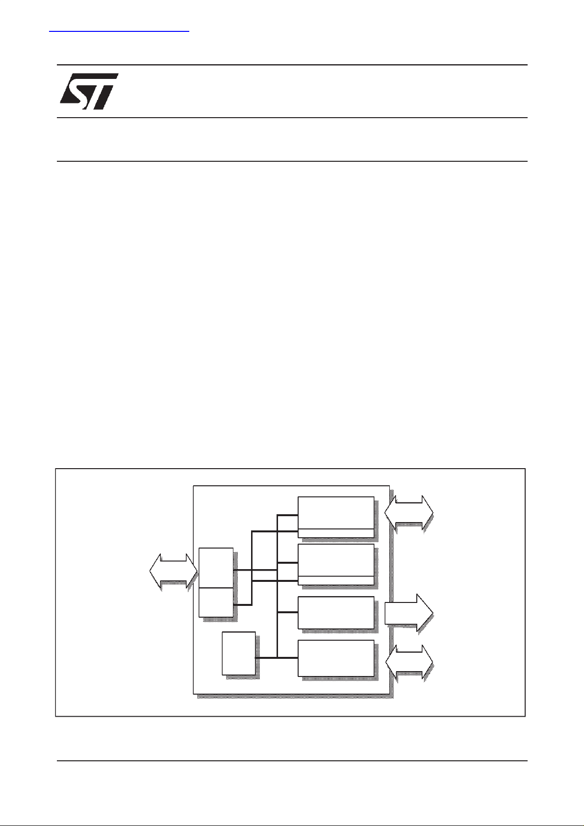
BLOCK DIAGRAM
PCI/AGP
1.6 GByte/s
Internal Bus
Bandwidth
Host
Interface
FIFO/
DMA
Pusher
VGA
DMA Bus
Internal Bus
Video Port
DMA Engine
Graphics Engine
128 bit 2D
Direct3D
DMA Engine
Palette DAC
YUV - RGB,
X & Y scaler
8MByte
SDRAM/SGRAM
Interface
CCIR656
Video
Monitor/
TV
128 bit
interface
June 1998
The information inthis datasheet is subject to change
7071857 00
1/85
Page 2

RIVA128ZX 128-BIT 3D MULTIMEDIA ACCELERATOR
TABLE OF CONTENTS
1 RIVA128ZX 300PBGA DEVICE PINOUT....................................................................................... 4
2 PIN DESCRIPTIONS ...................................................................................................................... 5
2.1 ACCELERATED GRAPHICS PORT (AGP) INTERFACE..................................................... 5
2.2 PCI 2.1 LOCALBUS INTERFACE........................................................................................ 5
2.3 FRAMEBUFFER INTERFACE .............................................................................................. 7
2.4 VIDEO PORT......................................................................................................................... 7
2.5 DEVICE ENABLE SIGNALS.................................................................................................. 8
2.6 DISPLAY INTERFACE.......................................................................................................... 8
2.7 VIDEO DAC AND PLL ANALOG SIGNALS .......................................................................... 8
2.8 POWER SUPPLY..................................................................................................................8
2.9 TEST...................................................................................................................................... 9
3 OVERVIEW OF THE RIVA128ZX .................................................................................................. 10
3.1 BALANCED PC SYSTEM...................................................................................................... 10
3.2 HOST INTERFACE ............................................................................................................... 10
3.3 2D ACCELERATION............................................................................................................. 11
3.4 3D ENGINE ........................................................................................................................... 11
3.5 VIDEO PROCESSOR............................................................................................................ 11
3.6 VIDEO PORT......................................................................................................................... 12
3.7 DIRECT RGB OUTPUT TO LOW COSTPAL/NTSC ENCODER ......................................... 12
3.8 SUPPORT FOR STANDARDS.............................................................................................. 12
3.9 RESOLUTIONS SUPPORTED.............................................................................................. 12
3.10 CUSTOMER EVALUATION KIT............................................................................................ 13
3.11 TURNKEY MANUFACTURING PACKAGE........................................................................... 13
4 ACCELERATED GRAPHICS PORT (AGP) INTERFACE ............................................................. 14
4.1 RIVA128ZX AGP INTERFACE.............................................................................................. 15
4.2 AGP BUS TRANSACTIONS.................................................................................................. 15
5 PCI 2.1 LOCAL BUS INTERFACE................................................................................................. 23
5.1 RIVA128ZX PCI INTERFACE ............................................................................................... 23
5.2 PCI TIMING SPECIFICATION............................................................................................... 24
6 FRAMEBUFFER INTERFACE ....................................................................................................... 30
6.1 SDRAM INTERFACE ............................................................................................................ 31
6.2 SGRAM INTERFACE............................................................................................................ 32
6.3 SDRAM/SGRAM ACCESSES AND COMMANDS................................................................ 35
6.4 LAYOUT OF FRAMEBUFFER CLOCK SIGNALS ................................................................ 37
6.5 FRAMEBUFFER INTERFACE TIMING SPECIFICATION.................................................... 37
7 VIDEO PLAYBACK ARCHITECTURE........................................................................................... 42
7.1 VIDEO SCALER PIPELINE................................................................................................... 43
8 VIDEO PORT.................................................................................................................................. 45
8.1 VIDEO INTERFACE PORT FEATURES............................................................................... 45
8.2 BI-DIRECTIONAL MEDIA PORT POLLING COMMANDSUSING MPC .............................. 46
8.3 TIMING DIAGRAMS.............................................................................................................. 47
8.4 656 MASTER MODE............................................................................................................. 51
8.5 VBI HANDLING IN THE VIDEO PORT ................................................................................. 52
8.6 SCALING IN THE VIDEO PORT........................................................................................... 52
9 BOOT ROM INTERFACE...............................................................................................................53
2/85
Page 3

128-BIT 3D MULTIMEDIA ACCELERATOR RIVA128ZX
10 POWER-ON RESET CONFIGURATION........................................................................................ 55
11 DISPLAY INTERFACE................................................................................................................... 57
11.1 PALETTE-DAC ...................................................................................................................... 57
11.2 PIXEL MODES SUPPORTED ............................................................................................... 57
11.3 HARDWARE CURSOR......................................................................................................... 58
11.4 SERIAL INTERFACE.............................................................................................................59
11.5 ANALOG INTERFACE .......................................................................................................... 60
11.6 TV OUTPUT SUPPORT........................................................................................................ 61
12 IN-CIRCUIT BOARD TESTING...................................................................................................... 63
12.1 TEST MODES ....................................................................................................................... 63
12.2 CHECKSUM TEST................................................................................................................63
13 ELECTRICAL SPECIFICATIONS .................................................................................................. 64
13.1 ABSOLUTE MAXIMUM RATINGS ........................................................................................ 64
13.2 OPERATING CONDITIONS.................................................................................................. 64
13.3 DC SPECIFICATIONS........................................................................................................... 64
13.4 ELECTRICAL SPECIFICATIONS.......................................................................................... 65
13.5 DAC CHARACTERISTICS .................................................................................................... 65
13.6 FREQUENCY SYNTHESIS CHARACTERISTICS................................................................ 66
14 PACKAGE DIMENSION SPECIFICATION.................................................................................... 67
14.1 300 PIN BALL GRID ARRAY PACKAGE .............................................................................. 67
15 REFERENCES................................................................................................................................ 68
16 ORDERING INFORMATION .......................................................................................................... 68
APPENDIX............................................................................................................................................... 69
A PCI CONFIGURATION REGISTERS............................................................................................. 69
A.1 REGISTER DESCRIPTIONS FOR PCI CONFIGURATION SPACE .................................... 69
3/85
Page 4
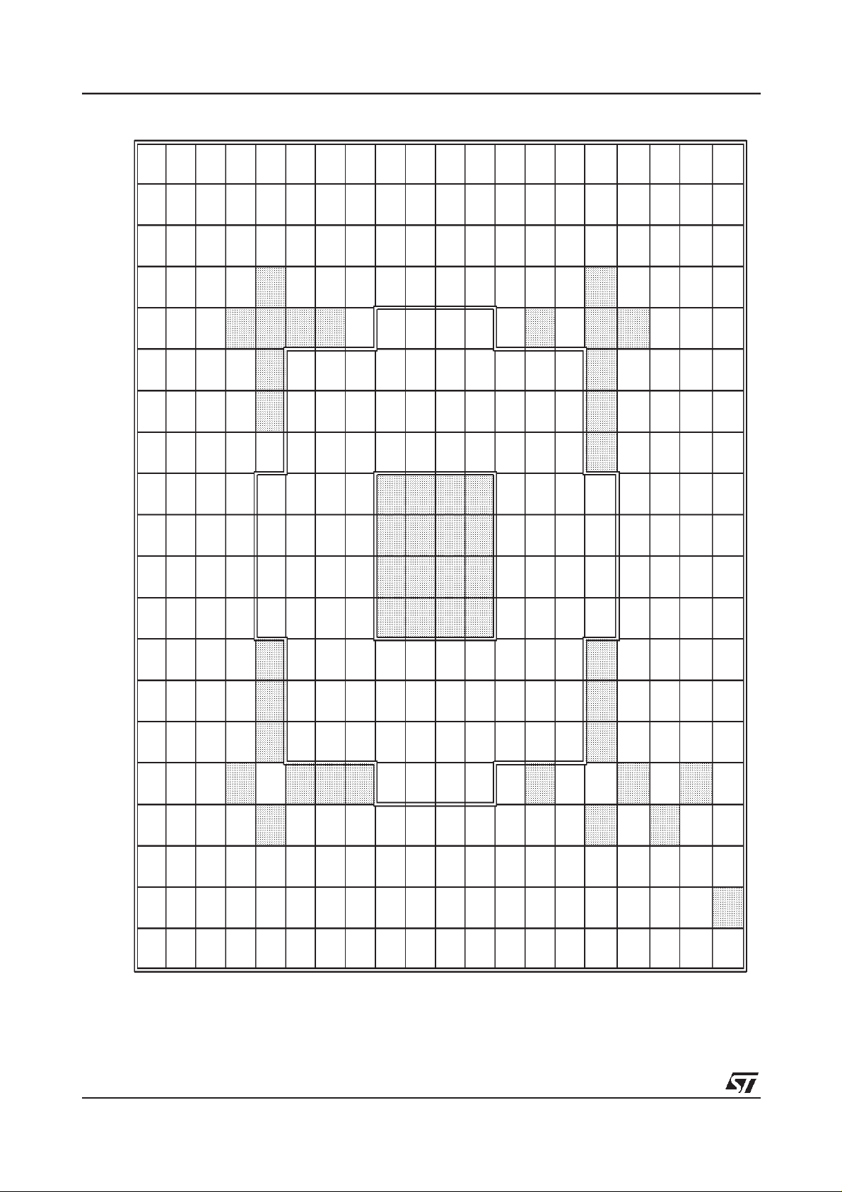
1 RIVA128ZX 300PBGA DEVICE PINOUT
∗ VDD VDD VDD VDD FBD[50] FBD[39] FBD[38]
FBCKE
128-BIT 3D MULTIMEDIA ACCELERATORRIVA128ZX
PCIAD[3] PCIAD[1]
STB0
AGPAD-
VDD FBD[97] FBD[127] FBD[126]
HOST-
CLAMP
HOSTVDD
HOST-
CLAMP
HOSTVDD
PCIAD[14] PCIAD[12] PCIAD[10] PCIAD[8]
PCI-
DEVSEL#
1234567891011121314151617181920
FBD[4] FBD[6] FBD[7] FBD[17] FBD[19] FBD[21] FBD[23] FBDQM[2] FBA[0] FBA[2] FBA[4] FBA[6] FBA[8] FBDQM[5] FBD[41] FBD[43] FBD[45] FBD[47] FBD[56] FBD[57]BFBD[3] FBD[5] FBD[16] FBD[18] FBD[20] FBD[22] FBDQM[0] FBA[9] FBA[1] FBA[3] FBA[5] FBA[7] FBCLK1 FBDQM[7] FBD[40] FBD[42] FBD[44] FBD[46] FBD[58] FBD[59]CFBD[1] FBD[2] FBD[28] FBD[27] FBD[26] FBD[25] FBD[15] FBD[13] FBD[11] FBD[9] FBDQM[1] FBWE# FBRAS# FBA[10] FBDQM[4] FBD[55] FBD[54] FBD[53] FBD[60] FBD[61]
A
FBCLK0 FBD[0] FBD[29] FBD[30] VDD FBD[24] FBD[14] FBD[12] FBD[10] FBD[8] FBDQM[3] FBCAS# FBCS0 FBCS1 FBDQM[6] VDD FBD[52] FBD[51] FBD[62] FBD[63]
D
SCL FBCLK2 FBD[31] VDD NIC VDD VDD VDD
E
MP_AD[6] NIC SDA FBCLKFB VDD VDD FBD[48] FBD[49] FBD[37] FBD[36]
F
MPFRAME# MP_AD[7] MP_AD[5] MP_AD[4] MPCLAMP VDD FBD[35] FBD[34] FBD[33] FBD[32]
G
MP_AD[2] MPSTOP# MPCLK MP_AD[3] VDD NIC FBDQM[12] FBDQM[14] FBDQM[15] FBDQM[13]
H
FBDQM[8] MPDTACK# MP_AD[1] MP_AD[0] GND GND GND GND FBD[118] FBD[119] FBD[105] FBD[104]KFBDQM[9] FBD[87] FBDQM[10] FBDQM[11] GND GND GND GND FBD[116] FBD[117] FBD[107] FBD[106]
J
NOTES
1 NIC = No Internal Connection. Do not connect to these pins.
2 VDD=3.3V
∗ Signals denotedwith an asterisk are defined for future expansion. See
HOST-
CLAMP
FBD[86] FBD[85] FBD[72] FBD[73] GND GND GND GND FBD[114] FBD[115] FBD[109] FBD[108]MFBD[84] FBD[83] FBD[74] FBD[75] GND GND GND GND FBD[112] FBD[113] FBD[111] FBD[110]NFBD[82] FBD[81] FBD[76] FBD[77] NIC NIC FBD[102] FBD[103] FBD[121] FBD[120]PFBD[80] FBD[71] FBD[78] FBD[79] VDD VDD FBD[100] FBD[101] FBD[123] FBD[122]RFBD[70] FBD[69] FBD[88] FBD[89] NIC NIC FBD[98] FBD[99] FBD[125] FBD[124]TFBD[68] FBD[67] FBD[90] VDD NIC HOSTVDD HOSTVDD
L
Pin Descriptions
, Section 2, page5 for details.
XTALOUT PCIRST# AGPST[1] PCIAD[30] PCIAD[26] PCICBE#[3] PCIAD[20] PCIAD[16] PCITRDY# PCIPAR HOSTVDD PCICBE#[0] FBD[96] VIDVSYNC VIDHSYNC
HOST-
CLAMP
FBD[66] FBD[65] FBD[92] FBD[91]
U
PCIAD[21] PCIAD[17] PCIIRDY# PCICBE#[1] PCIAD[13] PCIAD[9] PCIAD[4] PCIAD[0] PCIAD[7] PCIAD[5]
STB1
AGPAD-
FBD[64] FBD[95] RED DACVDD VREF PCIINTA# PCIGNT# AGPPIPE# PCIAD[28] PCIAD[24] PCIAD[22] PCIAD[18] PCIFRAME# PCISTOP# PCIAD[15] PCIAD[11] PCIAD[6] PCIAD[2] TESTMODE ROMCS#WFBD[93] FBD[94] BLUE COMP PLLVDD PCIREQ# AGPST[2] PCIAD[31] PCIAD[27]
V
PCIAD[29] PCIAD[25] PCIAD[23] PCIAD[19] PCICBE#[2]
AGPRBF#
PCIIDSEL/
GREEN GND RSET XTALIN PCICLK AGPST[0]
Y
4/85
Page 5

128-BIT 3D MULTIMEDIA ACCELERATOR RIVA128ZX
2 PIN DESCRIPTIONS
2.1 ACCELERATED GRAPHICS PORT (AGP) INTERFACE
Signal I/O Description
AGPST[2:0] I AGP status bus providing information fromthe arbiter to the RIVA128ZXon what it may
do. AGPST[2:0] only havemeaning to the RIVA128ZXwhen PCIGNT# is asserted. When
PCIGNT# is de-asserted these signals have no meaning and must beignored.
000 Indicates that previouslyrequested low priority read or flushdata is being
returned to the RIVA128ZX.
001 Indicates that previouslyrequested high priority readdata is being returned to
the RIVA128ZX.
010 Indicates that the RIVA128ZX is to provide low priority write data fora previous
enqueued write command.
011 Indicates that the RIVA128ZXis to provide high priority write data for a previous
enqueued write command.
100 Reserved
101 Reserved
110 Reserved
111 Indicates that the RIVA128ZX has been given permission to start a bus transac-
tion. The RIVA128ZXmay enqueue AGP requests by asserting AGPPIPE#or
start a PCI transaction by asserting PCIFRAME#. AGPST[2:0] are always an
output from the Core Logic (AGPchipset) and an input to the RIVA128ZX.
AGPRBF# O Read Buffer Full indicates when the RIVA128ZXis ready to accept previously requested
low priority read dataor not. When AGPRBF# is asserted the arbiter is not allowed to
return (low priority) read data to the RIVA128ZX.This signal should be pulled upvia a
4.7KΩ resistor (although it is supposed to be pulled up by the motherboard chipset).
AGPPIPE# O Pipelined Read is asserted byRIVA128ZX (when the current master) to indicate afull
width read addressis to be enqueued by the target.The RIVA128ZXenqueues one
request each rising clockedge while AGPPIPE#is asserted. When AGPPIPE#is deasserted no new requests are enqueued across PCIAD[31:0]. AGPPIPE# is a sustained
tri-state signal from the RIVA128ZXand is an inputto the target (the core logic).
AGPADSTB0,
AGPADSTB1
I/O Bus strobe signals providing timing for AGP2X data transfermode on PCIAD[15:00] and
PCIAD[31:16] respectively. The agent that is supplying data drives these signals.
2.2 PCI 2.1 LOCAL BUS INTERFACE
Signal I/O Description
PCICLK I PCI clock. This signal provides timing forall transactions on the PCI bus, except for
PCIRST# and PCIINTA#. All PCI signals are sampled on the rising edgeof PCICLK and
all timing parametersare defined with respect to this edge.
PCIRST# I PCI reset. This signal is used to bring registers, sequencers and signalsto a consistent
state. When PCIRST# is asserted all output signals are tristated.
PCIAD[31:0] I/O 32-bit multiplexedaddress and data bus. A bus transactionconsists of anaddress phase
followedby one or more data phases.
5/85
Page 6

128-BIT 3D MULTIMEDIA ACCELERATORRIVA128ZX
Signal I/O Description
PCICBE[3:0]# I/O Multiplexedbus command and byte enable signals. During the address phase of a trans-
action PCICBE[3:0]# define the bus command, during the data phase PCICBE[3:0]# are
used as byte enables. The byte enables are validfor theentire data phase and determine
which bytelanes contain validdata. PCICBE[0]# applies tobyte 0 (LSB) and PCICBE[3]#
applies to byte 3 (MSB).
When connectedto AGPthese signals carry differentcommands thanPCI whenrequests
are beingenqueued using AGPPIPE#. Validbyte information isprovided during AGPwrite
transactions. PCICBE[3:0]# are not used during the return of AGP read data.
PCIPAR I/O Parity.This signal is the evenparity bit generated across PCIAD[31:0] and
PCICBE[3:0]#. PCIPAR is stable and valid one clock after the address phase. For data
phases PCIPAR is stable and validone clock after either PCIIRDY# is asserted on a write
transaction or PCITRDY# is asserted on a read transaction. OncePCIPARis valid, it
remains validuntil one clock after completion ofthe currentdataphase. The masterdrives
PCIPARfor address and write data phases; the target drives PCIPAR for read data
phases.
PCIFRAME# I/O Cycle frame.This signal is driven by the current master to indicate the beginning of an
access and itsduration. PCIFRAME# is asserted to indicate that a bustransaction is
beginning. Data transferscontinue whilePCIFRAME# is asserted. When PCIFRAME# is
deasserted, the transaction is in the finaldata phase.
PCIIRDY# I/O Initiator ready.This signalindicates theinitiator’s(bus master’s)ability to completethe cur-
rent data phase of the transaction. See extended description for PCITRDY#.
When connected toAGP this signal indicates theinitiator (AGPcompliant master) isready
to provideall write datafor the current transaction. Once PCIIRDY# is asserted for a write
operation, the master is not allowed to insert wait states. The assertion ofPCIIRDY# for
reads, indicates that the master is ready to transfera subsequent block of read data. The
master is never allowedto insert a wait state during the initial blockof a read transaction.
However, it may insert wait states after each blocktransfers.
PCITRDY# I/O Targetready. This signal indicates thetarget’s (selected device’s) ability to complete the
current data phaseof the transaction.
PCITRDY# is used in conjunction withPCIIRDY#. A data phase is completedon any clock
when both PCITRDY# and PCIIRDY# are sampled as being asserted. During a read,
PCITRDY# indicates that valid data ispresent on PCIAD[31:0]. During a write,it indicates
the target is prepared to accept data. Wait cycles are inserted until both PCIIRDY# and
PCITRDY# are asserted together.
When connectedtoAGP thissignal indicates theAGP complianttarget is ready to provide
read data for the entire transaction (when transaction cancomplete within four clocks) or
is ready to transfera (initialor subsequent) block of data, when the transfer requiresmore
than four clocks to complete. The target is allowed to insert wait states after each block
transfers on both read and write transactions.
PCISTOP# I/O PCISTOP# indicates that the current target is requesting the master to terminate the cur-
rent transaction.
PCIIDSEL I Initialization device select. This signal is used as a chip select during configuration read
and write transactions.
For AGP applicationsnote that IDSEL isnot a pin on the AGP connector. The RIVA128ZX
performs the deviceselect decode internally within its host interface. It is not required to
connect the AD16signal to the IDSEL pin as suggested in the AGP specification.
PCIDEVSEL# I/O Deviceselect. Whenacting as an output PCIDEVSEL#indicates that the RIVA128ZX has
decoded the PCI address and isclaiming the current access as the target. As an input
PCIDEVSEL# indicates whetherany other device on the bushas been selected.
PCIREQ# O Request. This signalis asserted by the RIVA128ZXto indicateto the arbiter that it desires
to become master of the bus.
6/85
Page 7
128-BIT 3D MULTIMEDIA ACCELERATOR RIVA128ZX
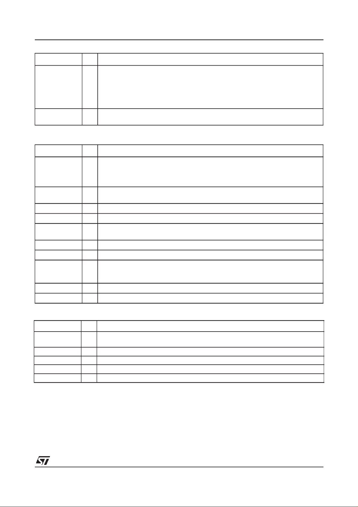
Signal I/O Description
PCIGNT# I Grant. This signal indicates to the RIVA128ZX that access to the bus has been granted
and it can now become bus master.
When connectedto AGPadditional information isprovided on AGPST[2:0] indicating that
the master is the recipient of previously requested read data (high or low priority), it is to
provide write data (high or low priority), for a previously enqueued write command or has
been given permission to start a bus transaction (AGP or PCI).
PCIINTA# O Interrupt request line. This opendrain output is asserted and deasserted asynchronously
to PCICLK.
2.3 FRAMEBUFFER INTERFACE
Signal I/O Description
FBD[127:0] I/O The 128-bitmemory data bus.
FBD[31:0] are also used to access up to 64KBytes of 8-bit ROM or Flash ROM, using
FBD[15:0] as address ROMA[15:0], FBD[31:24] as ROMD[7:0], FBD[17] as ROMWE#
and FBD[16] as ROMOE#.
FBA[10:0] O Memory Address bus. Configuration strapping options are also decoded on thesesignals
during PCIRST# as described in Section 10, page 55.
FBRAS# O Memory RowAddress Strobe forall memory devices.
FBCAS# O Memory ColumnAddress Strobe for all memory devices.
FBCS[1:0]# O Memory Chip Select strobes. For SDRAM the FBCS[1] pin providesthe memory’s inter-
nal bank select bit (BA/A11).
FBWE# O Memory Write Enablestrobe forall memory devices.
FBDQM[15:0] O Memory Data/Output Enable strobes.
FBCLK0,
FBCLK1,
FBCLK2
FBCLKFB I Framebuffer clock feedback. FBCLK2 is fed back to FBCLKFB.
FBCKE O Framebuffermemory clock enablesignal.
O Memory Clock signals. Separate clocksignals FBCLK0 and FBCLK1 are providedfor
each bank of memory forreduced clock skew and loading. Details ofrecommended memory clock layout are given in Section 6.4, page 37.
2.4 VIDEO PORT
Signal I/O Description
MP_AD[7:0] I/O Media Port 8-bit multiplexedaddress and data bus or ITU-R-656 video data bus when in
656 mode.
MPCLK I 40MHz Media Port system clock or pixelclock when in 656 mode.
MPDTACK# I Media Port data transferacknowledgmentsignal.
MPFRAME# O Initiates Media Port transfers when active, terminates transferswhen inactive.
MPSTOP# I Media Port control signal used by the slave to terminate transfers.
7/85
Page 8
128-BIT 3D MULTIMEDIA ACCELERATORRIVA128ZX
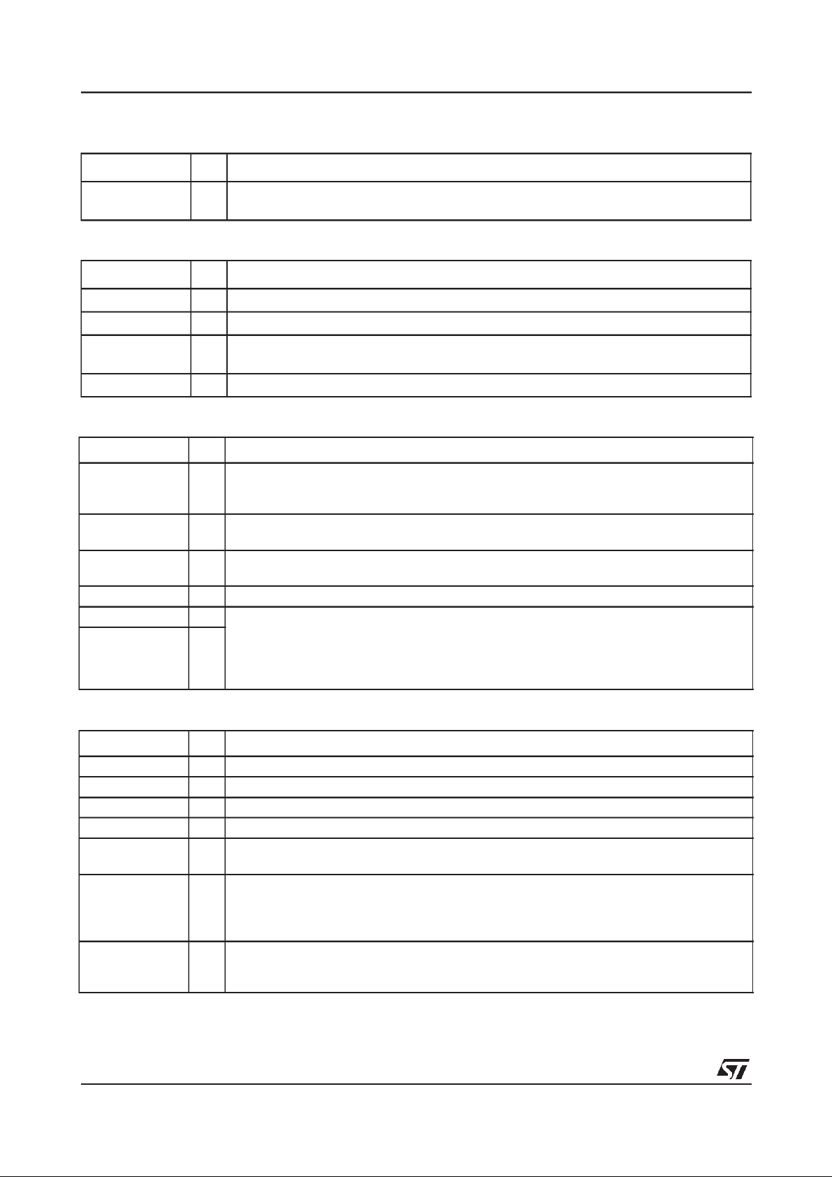
2.5 DEVICE ENABLE SIGNALS
Signal I/O Description
ROMCS# O Enables reads from an external 64Kx 8 or 32Kx8 ROM or Flash ROM. This signalis used
in conjunction with framebuffer data lines as described abovein Section 2.3.
2.6 DISPLAY INTERFACE
Signal I/O Description
SDA I/O Used forDDC2B+ monitor communication and interface to video decoder devices.
SCL I/O Used forDDC2B+ monitor communication and interface to video decoder devices.
VIDVSYNC O Vertical sync supplied to thedisplay monitor.No bufferingis required. In TV mode this sig-
nal supplies composite sync to an external PAL/NTSCencoder.
VIDHSYNC O Horizontal sync supplied to the display monitor. No buffering is required.
2.7 VIDEO DAC AND PLL ANALOG SIGNALS
Signal I/O Description
RED,
GREEN,
BLUE
COMP - External compensation capacitor for the video DACs. This pin should be connected to
RSET - A precision resistor placed between this pin and GND sets the full-scale video DAC cur-
VREF - A capacitor should beplaced between this pin and GND as shown in Figure 66, page 60.
XTALIN I A series resonantcrystal is connected between these two points to provide the reference
XTALOUT O
O RGB display monitor outputs. These are software configurableto drive either a doubly ter-
minated or singly terminated 75Ω load.
DACVDD via the compensation capacitor, see Figure 66, page 60.
rent, see Figure66, page 60.
clock forthe internal MCLK andVCLK clock synthesizers,see Figure 66 and Table20,
page 60. Alternately, an externalLVTTLclock oscillator output may be driven into XTA-
LOUT, connecting XTALIN to GND.For designs supporting TV-out,XTALOUT should be
driven by a reference clock as described in Section 11.6, page 61.
2.8 POWER SUPPLY
Signal I/O Description
DACVDD P Analog power supply for the video DACs.
PLLVDD P Analog power supply forall clock synthesizers.
VDD P Digital power supply.
GND P Ground.
MPCLAMP P MPCLAMP is connected to +5V to protect the 3.3V RIVA128ZXfrom external devices
which will potentially drive 5V signal levels onto the Video Port input pins.
HOSTVDD P HOSTVDD is connected to the Vddq 3.3 pins on the AGP connector. This is the supply
voltage forthe I/O buffers and is isolated from the core VDD.On AGP designs these pins
are also connected to the HOSTCLAMP pins. On PCI designsthey are connected to the
3.3V supply.
HOSTCLAMP P HOSTCLAMP is the supply signalling rail protection for the host interface. In AGPdesigns
these signals areconnected to Vddq 3.3. For PCI designs they are connected to the I/O
power pins (V
8/85
(I/O)
).
Page 9

128-BIT 3D MULTIMEDIA ACCELERATOR RIVA128ZX
2.9 TEST
Signal I/O Description
TESTMODE I For designs which will be tested in-circuit, this pin should be connected toGND through a
10KΩ pull-down resistor, otherwise this pin should be connected directly to GND.When
TESTMODE is asserted, MP_AD[3:0] are reassigned as TESTCTL[3:0] respectively.
Information on in-circuit test is given in Section 12, page 63.
9/85
Page 10

128-BIT 3D MULTIMEDIA ACCELERATORRIVA128ZX
3 OVERVIEW OF THE RIVA128ZX
The RIVA128ZX is the first 128-bit 3D Multimedia
Accelerator to offer unparalleled 2D and 3D performance, meeting all the requirements of the
mainstream PC graphics market and Microsoft’s
PC’97. The RIVA128ZX introduces the most advanced Direct3D acceleration solution and also
delivers leadership VGA, 2D and Video performance, enabling a range of applications from 3D
games throughto DVD, Intercast and video conferencing.
3.1 BALANCED PC SYSTEM
The RIVA128ZX is designed to leverage existing
PC system resources such as system memory,
high bandwidth internal buses and bus master capabilities. The synergy between the RIVA128ZX
graphics pipeline architecture and that of the current generationPCI andnext generation AGPplatforms, defines ground breaking performance levels at the cost point currently required for mainstream PC graphics solutions.
Execute versus DMA models
The RIVA128ZXis architectedto optimize PC system resources in a manner consistent with the
AGP “Execute” model. In this model texturemap
data for 3D applications is stored in system memory and individual texels are accessed as needed
by the graphics pipeline. This is a significant enhancement over the DMA model where entire texture maps are transferred into off-screen framebuffer memory.
The advantages of the Execute versus the DMA
model are:
• Improved system performance since only the
required texels and not the entire texture map,
cross the bus.
• Substantial cost savings since all the frame-
buffer is usable for the displayed screen and Z
buffer andno part of it is required to be dedicated to texture storage or texture caching.
• There is no software overhead in the Direct3D
driver to manage texture caching between application memory and the framebuffer.
To extend the advantages of the Execute model,
the RIVA128ZX’s proprietary texture cache and
virtual DMA bus master design overcomes the
bandwidth limitation of PCI, by sustaining a high
texel throughput with minimum bus utilization.The
host interface supports burst transactions up to
133MHz and provides over 400MBytes/s onAGP.
AGP accesses offer other performance enhancements sincethey are fromnon-cacheable memory
(no snoop) and can be low priority to prevent processor stalls, or high priority to prevent graphics
engine stalls.
Building a balanced system
RIVA128ZX is architected to provide the level of
3D graphics performance and quality available in
top arcade platforms. To provide comparable
scene complexity in the 1997 time-frame, processors will have to achieve new levels of floating
point performance. Profiles have shown that 1997
mainstream CPUs will be able to transform over 1
million lit, meshed triangles/s at50% utilization using Direct3D. This represents an order of magnitude performance increase over anything attainable in 1996 PC games.
To build a balanced system the graphics pipeline
must match the CPU’sperformance.It mustbe capable of rendering at least 1 million polygons/s in
order to avoid CPU stalls. Factors affecting this
system balance include:
• Direct3D compatibility. Minimizing the differ-
ences between the hardware interface and the
Direct3D data structures.
• Triangle setup. Minimizing the number of for-
mat conversionsand delta calculations done by
the CPU.
• Display-list processing. Avoiding CPU stalls by
allowing the graphics pipeline to execute independently of the CPU.
• Vertex caching. Avoids saturating the host in-
terface withrepeated vertices, lowering thetraffic onthe busandreducing systemmemory collisions.
• Host interface performance.
3.2 HOST INTERFACE
The host interfaceboosts communicationbetween
the host CPU and the RIVA128ZX. The optimized
interface performs burst DMA bus mastering for
efficient and fast data transfer.
• 32-bit PCI version 2.1 or AGP version 1.0
• Burst DMA Master and target
• 33MHz PCI clock rate, 66MHz AGP clock rate
and AGP 2X mode
• Supports over 100MBytes/s with33MHz PCI to
over 400MBytes/s on AGP 2X mode
• Implements read buffer posting on AGP
10/85
Page 11

128-BIT 3D MULTIMEDIA ACCELERATOR RIVA128ZX
•
Fully supportsthe “Execute” modelon both PCI
and AGP
3.3 2D ACCELERATION
The RIVA128ZX’s 2D rendering engine delivers
industry-leading Windows acceleration performance:
• 100MHz 128-bit graphics engine optimized for
single cycle operation into the 128-bit memory
interface supporting up to 1.6GBytes/s
• Acceleration functions optimized for minimal
software overhead on key GDI calls
• Extensive support for DirectDraw in
Windows95 including optimized Direct Framebuffer (DFB) access with Write-combining
• Accelerated primitives including BLT, transpar-
ent BLT, stretchBLT, points, lins, lines,
polylines, polygons, fills, patterns, arbitrary
rectangular clipping and improved text rendering
• Pipeline optimized for multiple color depths in-
cluding 8, 15, 24, and 30 bits per pixel
• DMA Pusher allows the 2Dgraphics pipeline to
load rendering methods optimizing
RIVA128ZX/host multi-tasking
• Execution of all 256 Raster Operations (as de-
fined by Microsoft Windows) at 8, 15, 24 and
30-bit color depths
• 15-bit hardware color cursor
• Hardware color dithering
• Multi buffering (Double, Triple, Quad buffering)
for smooth animation
fers to Direct3D or similar APIs advanced triangle
rendering capabilities:
• Rendering pipeline optimized for Microsoft’s
Direct3D API
• Perspective correct true-color Gouraud lighting
and texture mapping
• Full 32-bit RGBA texture filter and Gouraud
lighting pixel data path
• Alpha blending for translucency and transpar-
ency
• Sub-pixel accurate texture mapping
• Internal pixel path: up to 24bits, alpha: up to 8
bits
• Texture magnification filtering with high quality
bilinear filtering without performance degradation
• Texture minification filtering with MIP mapping
without performance degradation
• LOD MIP-mapping: filter shape is dynamically
adjusted based on surface orientation
• Texture sizes from 4 to 2048 texels in either U
or V
• Textures can be looped and paged in real time
for texture animation
• Perspective correct per-pixel fog for atmo-
spheric effects
• Perspective correct specular highlights
• Multi buffering (Double, Triple, Quad buffering)
for smooth 3D animation
• Multipass rendering for environmental mapping
and advanced texturing
3.4 3D ENGINE
Triangle setup engine
• Setup hardware optimized for Microsoft’s
Direct3D API
• 5Gflop floating point geometry processor
• Slope and setup calculations
• Accepts IEEE Single Precision format used in
Direct3D
• Efficient vertex caching
Rendering engine
The RIVA128ZX Multimedia Accelerator integrates an orthodox 3D rendering pipeline and triangle setup function which not only fully utilizes
the capabilities of the Accelerated Graphics Port,
but also supports advanced texture mapped 3D
over the PCI bus. The RIVA128ZX 3D pipeline of-
3.5 VIDEO PROCESSOR
The RIVA128ZX Palette-DAC pipeline accelerates
full-motion video playback, sustaining 30 frames
per secondwhile retaining the highestquality color
resolution, implementing true bilinear filtering for
scaled video, and compensating for filtering losses
using edge enhancement algorithms.
• Advanced support for DirectDraw (DirectVideo)
in Windows 95
• Back-end hardwarevideo scalingfor video con-
ferencing and playback
• Hardware color space conversion (YUV 4:2:2
and 4:2:0)
• Multi-tap X and Y filtering for superior image
quality
• Optional edge enhancement to retain video
sharpness
11/85
Page 12
Supportfor scaledfield interframingfor reduced
•
motion artifacts and reduced storage
• Per-pixel color keying
• Multiple video windows with hardware color
space conversion and filtering
• Planar YUV12 (4:2:0) to/from packed (4:2:2)
conversion for software MPEG acceleration
and H.261 video conferencing applications
• Accelerated playback of industry standard co-
decs including MPEG-1/2, Indeo, Cinepak
3.6 VIDEO PORT
The RIVA128ZX Multimedia Accelerator provides
connectivity forvideo input devices suchas Philips
SAA7111A, ITT 3225 and Samsung KS0127
through an ITU-R-656 video input bus to DVD and
MPEG2 decodersthrough bidirectional mediaport
functionality.
• Supported through VPE extensions to Direct-
Draw
• Supports filtered down-scaling and decimation
• Supports real time video capture via Bus Mas-
tering DMA
• Serial interface for decoder control
128-BIT 3D MULTIMEDIA ACCELERATORRIVA128ZX
3.7 DIRECT RGB OUTPUT TO LOW COST
PAL/NTSC ENCODER
The RIVA128ZX has also been designed to interface to a standard PAL or NTSC television via a
low cost TVencoder chip. InPAL or NTSC display
modes the interlaced output is internally flicker-filtered and CCIR/EIA compliant timing reference
signals are generated.
3.8 SUPPORT FOR STANDARDS
• Multimedia support for MS-DOS, Windows
3.11, Windows 95, and Windows NT
• Acceleration for Windows 95 Direct APIs in-
cluding Direct3D, DirectDraw and DirectVideo
• VGA and SVGA: The RIVA128ZX has an in-
dustry standard32-bit VGAcore andBIOS support. In PCI configuration space the VGA can
be enabled and disabled independently of the
GUI.
• Glue-less Accelerated Graphics Port (AGP 1.0)
or PCI 2.1 bus interface
• ITU/CCIR-656 compatible video port
• VESA DDC2B+, DPMS, VBE 2.0 supported
3.9 RESOLUTIONS SUPPORTED
Resolution BPP 2MByte 4MByte (128-bit) 8MByte (64-bit) 8MByte (128-bit)
4 120Hz 120Hz 120Hz 120Hz
640x480
800x600
1024x768
1152x864
1280x1024
1600x1200
1920x1080
1920x1200
1800x1440 16 - - 60Hz 60Hz
8 120Hz 120Hz 120Hz 120Hz
16 120Hz 120Hz 120Hz 120Hz
32 120Hz 120Hz 120Hz 120Hz
8 120Hz 120Hz 120Hz 120Hz
16 120Hz 120Hz 120Hz 120Hz
32 120Hz 120Hz 120Hz 120Hz
8 120Hz 120Hz 120Hz 120Hz
16 120Hz 120Hz 120Hz 120Hz
32 - 120Hz 120Hz 120Hz
8 120Hz 120Hz 120Hz 120Hz
16 120Hz 120Hz 120Hz 120Hz
32 - 100Hz 100Hz 100Hz
8 100Hz 100Hz 100Hz 100Hz
16 - 100Hz 100Hz 100Hz
32 - - t.b.d. 75Hz
8 85Hz 85Hz 85Hz 85Hz
16 - 85Hz 85Hz 85Hz
32 - - - 60Hz
8 - 85Hz 85Hz 85Hz
16 - - 85Hz 85Hz
8 - 75Hz 75Hz 75Hz
16 - - 75Hz 75Hz
12/85
Page 13

128-BIT 3D MULTIMEDIA ACCELERATOR RIVA128ZX
3.10 CUSTOMER EVALUATION KIT
A Customer Evaluation Kit (CEK) is available for
evaluating the RIVA128ZX. The CEK includes a
PCI or AGP adapter card designed to support the
RIVA128ZX feature set, an evaluation CD-ROM
containing afast-installation application, extensive
device drivers and programs demonstrating the
RIVA128ZX features and performance.
This CEK includes:
• RIVA128ZX evaluation board and CD-ROM
• QuickStart install/user guide
• OS drivers and files
- Windows 3.11
- Windows 95 Direct X/3D
- Windows NT 3.5
- Windows NT 4.0
• Demonstration files and Game demos
• Benchmark programs and files
3.11 TURNKEY MANUFACTURING PACKAGE
A Turnkey Manufacturing Package (TMP) isavail-
able to support OEM designs and development
through to production. It delivers a complete manufacturable hardware and software solution that
allows an OEM to rapidly design and bring to volume an RIVA128ZX-based product.
This TMP includes:
• CD-ROM
- RIVA128ZX Datasheet and Application
Notes
- OrCAD schematic capture and PADS
layout design information
- Quick Start install/user guide/releasenotes
- BIOS Modification program, BIOS binaries,
utilities and BIOS Modification Guide documentation
- Bring-up and OEM Production Diagnostics
- Software and Utilities
• OS drivers and files
- Windows 3.11
- Windows 95 Direct X/3D
- Windows NT 3.5
- Windows NT 4.0
• Content developer and WWW information
• Partner solutions
• Access to our password-protected web site for
upgrade files and release notes.
13/85
Page 14
128-BIT 3D MULTIMEDIA ACCELERATORRIVA128ZX
4 ACCELERATED GRAPHICS PORT (AGP) INTERFACE
The AcceleratedGraphics Port (AGP) is ahigh performance,component level interconnecttargeted at3D
graphical display applications and based on performance enhancements to the PCI local bus.
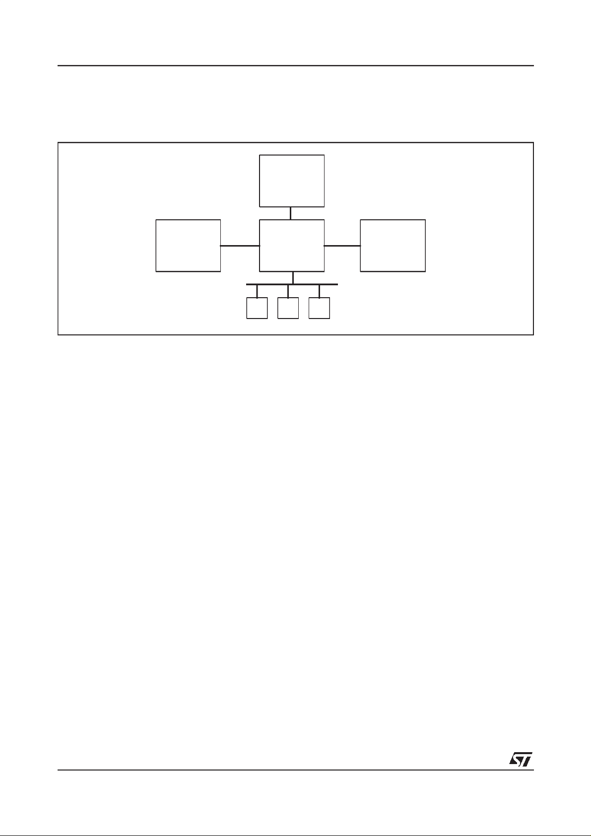
Figure 1. System block diagram showing relationship between AGP and PCI buses
CPU
AGP
AGP chipsetRIVA128ZX
PCI
I/O I/O I/O
Background to AGP
Although 3D graphics acceleration is becoming a
standard feature of multimedia PC platforms, 3D
rendering generally has a voracious appetite for
memory bandwidth.Consequently thereis upward
pressure onthe PC’s memory requirement leading
to higher billof materialcosts. These trends will increase, requiring high speed access to larger
amounts of memory. The primary motivation for
AGP therefore was to contain these costs whilst
enabling performance improvements.
By providing significant bandwidth improvement
between the graphics accelerator and system
memory, someof the3D renderingdata structures
can be shifted into main memory, thus relieving
the pressure to increase the cost of the local
graphics memory.
Texture data are the first structures targeted for
shifting to system memory for four reasons:
1 Textures are generally read only, and therefore
do not have special access ordering or coherency problems.
2 Shifting textures balances the bandwidth load
between system memory and local graphics
memory, since a well cached host processor
has much lower memory bandwidth requirements than a 3D rendering engine. Texture accesscomprises perhapsthe largestsingle component of rendering memory bandwidth (compared with rendering,display and Z buffers), so
avoiding loading or cachingtexturesin graphics
System
memory
local memory saves not only this component of
local memory bandwidth, but also the bandwidth necessary to load the texture store in the
first place. Furthermore, this data must pass
through main memory anyway as it is loaded
from a mass store device.
3 Texture size is dependent upon application
quality rather than on display resolution, and
therefore subject to the greatest pressure for
growth.
4 Texture data is not persistent; it resides in
memory only for the duration of the application,
so any system memory spent on texture storage can be returned to the free memory heap
when the application finishes (unlike display
buffers which remain in use).
Other data structures can be moved tomain memory but the biggest gain results from moving texture data.
Relationship of AGP to PCI
AGP is a superset of the 66MHzPCI Specification
(Revision 2.1) with performance enhancements
optimized for highperformance 3D graphics applications.
The PCI Specification is unmodified by AGP and
‘reserved’ PCI fields, encodings and pins, etc. are
not used.
AGP does not replace the need for the PCI bus in
the system and the two are physically, logically,
and electrically independent.As shown in Figure1
14/85
Page 15

128-BIT 3D MULTIMEDIA ACCELERATOR RIVA128ZX
the AGP bridge chip and RIVA128ZX are the only
devices on theAGP bus - all other I/O devices remain on the PCI bus.
The add-in slot defined for AGP uses a new connector body (for electrical signaling reasons)
which is not compatible with the PCI connector;
transactions, where the address, wait and data
phases need to complete before the next transaction starts. AGP transactionscan only accesssystem memory - not other PCI devices or CPU. Bus
mastering accesses can be either PCI or AGPstyle.
PCI and AGP boards are not mechanically interchangeable.
AGP accesses differ from PCI in that they are
pipelined. This compares with serialized PCI
Full details of AGP are given in the
Graphics Port InterfaceSpecification
by Intel Corporation.
4.1 RIVA128ZX AGP INTERFACE
The RIVA128ZX glueless interface to AGP1.0 is shown in Figure 2.
Figure 2. AGP interface pin connections
PCIAD[31:0]
32
PCICBE[3:0]#
4
AGPST[2:0]#
3
AGPRBF#
AGPPIPE#
PCIDEVSEL#
PCIIRDY#
AGP bus
PCITRDY#
PCISTOP#
PCIIDSEL
PCIPAR
PCIREQ#
PCIGNT#
PCICLK
PCIRST#
PCIINTA#
RIVA128ZX
Accelerated
[3] published
4.2 AGP BUS TRANSACTIONS
AGP bus commands supported
The following AGP bus commands are supported
by the RIVA128ZX:
- Read
- Read (hi-priority)
PCI transactions on the AGP bus
PCI transactions can be interleaved with AGP
transactions including between pipelined AGP
data transfers.A basic PCItransaction ontheAGP
interface is shown in Figure 3. If the PCI target is
a non AGP compliant master, it will not see
AGPST[2:0] and the transaction appears to be on
a PCI bus. For AGP aware bus masters,
AGPST[2:0] indicate thatpermission touse theinterface has been granted to initiate a request and
not to move AGP data.
15/85
Page 16
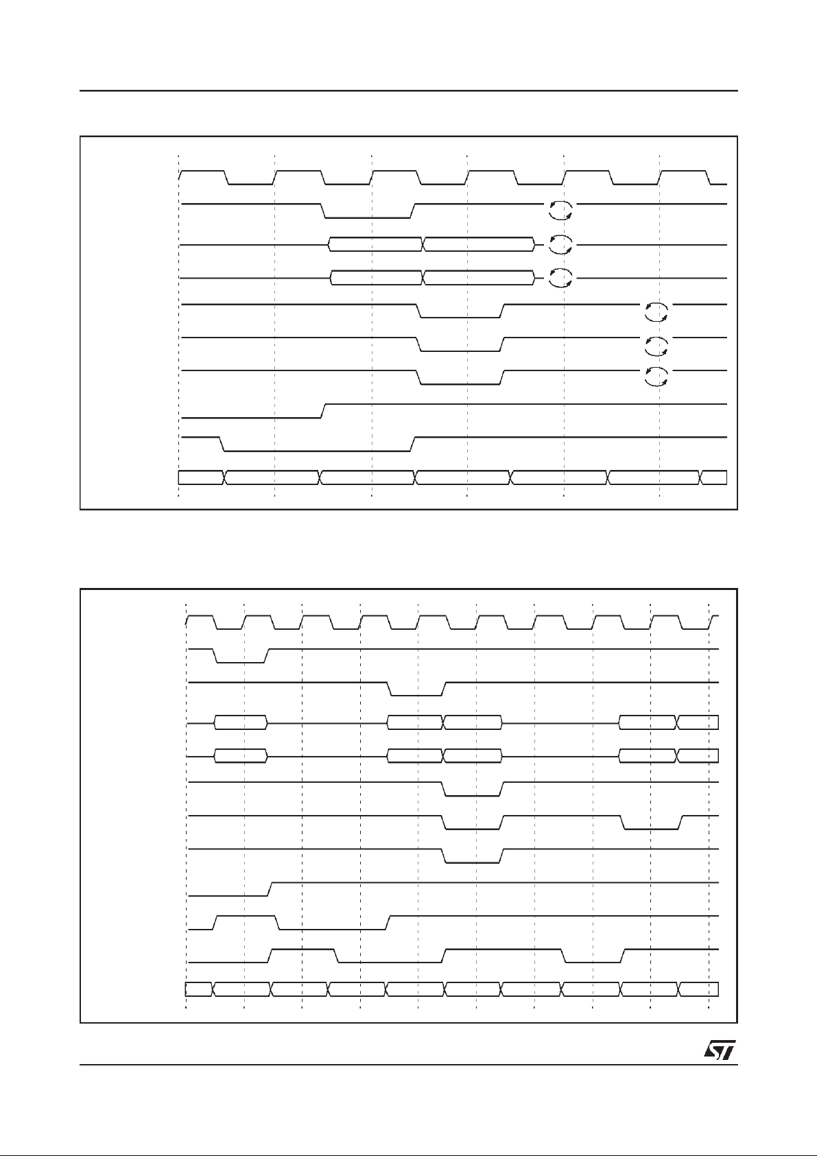
Figure 3. Basic PCI transaction on AGP
134562
PCICLK
PCIFRAME#
128-BIT 3D MULTIMEDIA ACCELERATORRIVA128ZX
PCIAD[31:0]
PCICBE[3:0]#
PCIIRDY#
PCITRDY#
PCIDEVSEL#
PCIREQ#
PCIGNT#
AGPST[2:0]
bus cmd
111 111 xxx xxx xxxxxx
data_pciaddress
BE[3:0]#
An example of a PCI transaction occurring between an AGP command cycle and return of data is shown
in Figure 4. This shows the smallest number of cycles during which an AGPrequest can be enqueued, a
PCI transaction performed and AGP read data returned.
Figure 4. PCI transaction occurring between AGP request and data
1 2345678910
PCICLK
AGPPIPE#
PCIFRAME#
PCIAD[31:0]
PCICBE#
PCIIRDY#
PCITRDY#
PCIDEVSEL#
PCIAGPRBF#
PCIREQ#
PCIGNT#
AGPST[2:0]
A9
C9 pci_cmd BE 0000 000
111 xxx 111 111 xxx111
address data D7 +1
xxx 00x xxx xxx
16/85
Page 17

128-BIT 3D MULTIMEDIA ACCELERATOR RIVA128ZX
Figure 5. Basic AGP pipeline concept
Bus Idle
Pipelined
data
transfer
Intervene
cycles
A1 A2
Pipelined AGP requests
Data-1 Data-2
Pipeline operation
Memory access pipelining provides the main performance enhancement of AGP over PCI. AGP
pipelined bus transactions share most of the PCI
signal set, and are interleaved with PCI transactions on thebus.
The RIVA128ZX supports AGP pipelined reads
with a 4-deep queue of outstanding read requests.
Pipelined reads are primarily used by the
RIVA128ZX for cache filling, the cache size being
optimized for AGP bursts. Depending on the AGP
bridge, abandwidth ofup to 248MByte/s isachievable for 128-byte pipelined reads. This compares
with around 100MByte/s for 128-byte 33MHz PCI
reads. Another feature of AGP is that for smaller
sized reads the bandwidth is not significantly reduced. Whereas 16-byte reads on PCI transfer at
around 33MByte/s, on AGP around 175MByte/s is
achievable. The RIVA128ZX actually requests
reads greater than 64 bytes in multiplesof 32-byte
transactions.
The pipedepth canbe maintained bythe AGP bus
master (RIVA128ZX) intervening in a pipelined
transfer to insert new requests between data replies. This bus sequencing is illustrated in Figure
5.
When the bus is in an idle condition, the pipe can
be started by inserting one or more AGP access
requests consecutively. Once the data reply to
those accesses starts, that stream can be broken
(or intervened) by the busmaster (RIVA128ZX) inserting one or more additional AGP access requests or inserting a PCI transaction. This intervention is accomplished with the bus ownership
signals, PCIREQ# and PCIGNT#.
Data-3
A3
A
Data
PCI transaction
The RIVA128ZX implements both high and low
priority reads depending of the status of the rendering engine. Ifthe pipeline is likely to stall due to
system memory read latency, a high priority read
request is posted.
Address Transactions
The RIVA128ZX requests permission from the
bridge to use PCIAD[31:0] to initiate either an
AGP request or a PCI transaction by asserting
PCIREQ#. The arbiter grants permission by asserting PCIGNT# with AGPST[2:0] equal to ”111”
(referred to as START). Whenthe RIVA128ZX receives START it must start thebus operation within two clocks of the bus becoming available. For
example, whenthe busis inan idle conditionwhen
START is received, the RIVA128ZX must initiate
the bus transaction on the next clock and the one
following.
Figure 6 shows a single address being enqueued
by the RIVA128ZX. Sometime before clock 1, the
RIVA128ZX asserts PCIREQ# to gain permission
to usePCIAD[31:0]. Thearbiter grants permission
by indicating START on clock 2. A new request
(address, command and length) are enqueued on
each clock in which AGPPIPE# is asserted. The
address of the request tobe enqueued is presented onPCIAD[31:3], thelength on PCIAD[2:0] and
the command on PCICBE[3:0]#. In Figure 6 only
a single address is enqueued since AGPPIPE# is
just asserted for a single clock. The RIVA128ZX
indicates that the current address is the last it intends to enqueue when AGPPIPE# is asserted
and PCIREQ# is deasserted (occurring on clock
3). Once the arbiter detects the assertion of AGP-
PIPE# or PCIFRAME# it deasserts PCIGNT# on
clock 4.
17/85
Page 18
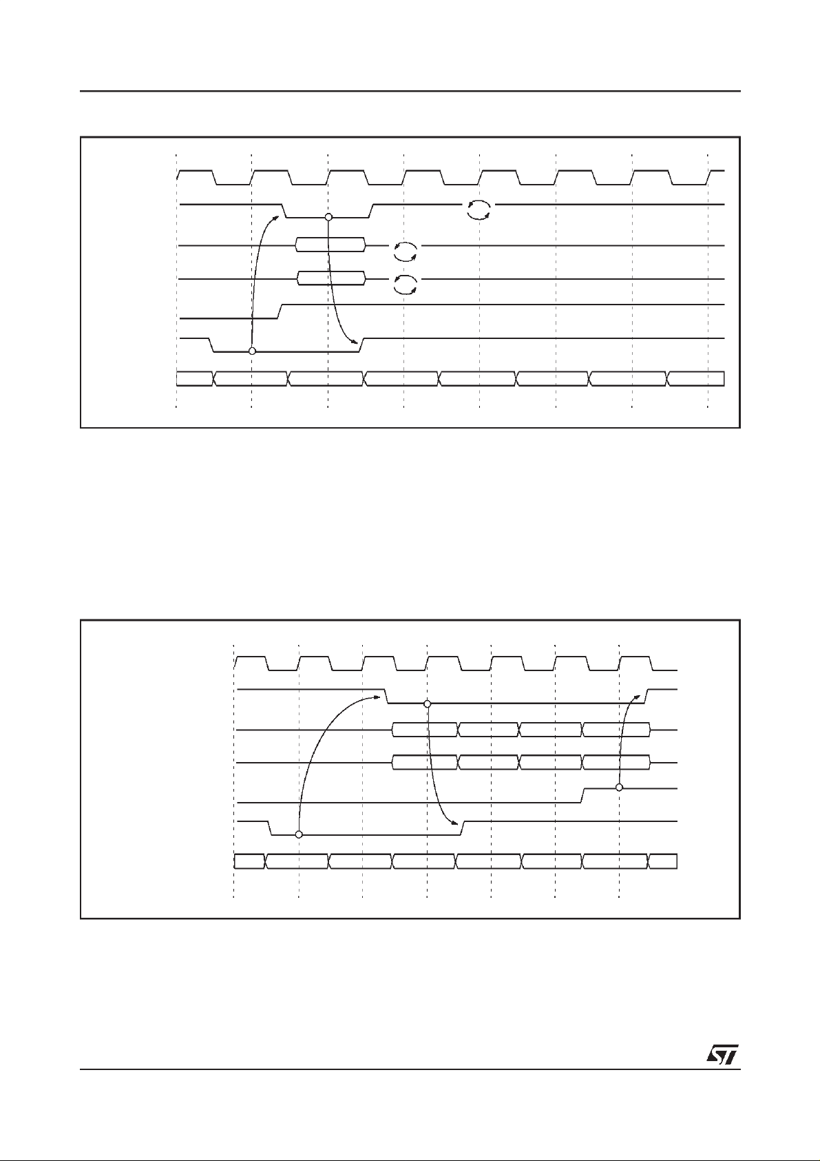
Figure 6. Single address - no delay by master
12345678
PCICLK
AGPPIPE#
128-BIT 3D MULTIMEDIA ACCELERATORRIVA128ZX
PCIAD[31:0]
PCICBE[3:0]#
PCIREQ#
PCIGNT#
AGPST[2:0]
111 111 xxx xxx xxxxxx xxx xxx
A1
C1
Figure 7 showsthe RIVA128ZXenqueuing 4 requests, where the first request is delayed bythe maximum
2 cycles allowed. START is indicated on clock 2, but the RIVA128ZX does not assert AGPPIPE# until
clock 4. Note that PCIREQ# remainsasserted on clock 6 toindicate that thecurrent request is not the last
one. When PCIREQ# is deasserted onclock 7 with AGPPIPE# still assertedthis indicates thatthe current
address is the last one tobe enqueuedduring thistransaction. AGPPIPE# must be deassertedon thenext
clock when PCIREQ# is sampled as deasserted. If the RIVA128ZXwants to enqueue more requestsduring this bus operation, itcontinues assertingAGPPIPE# until all ofits requests areenqueued or until it has
filled all the available request slots provided by the target.
Figure 7. Multiple addresses enqueued, maximum delay by RIVA128ZX
1234567
PCICLK
AGPPIPE#
PCIAD[31:0]
PCICBE#
PCIREQ#
PCIGNT#
AGPST[2:0]
A1
C1 C2 C3 C4
111 111 111 xxx xxxxxx xxx xxx
A2 A3 A4
2X Data Transfers
2X data transfers are similar to 1X transfers except that an entire 8 bytes are transferred during a single
PCICLK period. This requires that two 4 byte pieces of data are transferred acrossPCIAD[31:0] for each
CLK period. A read data transfer is described followed by awrite transfer.
18/85
Page 19
128-BIT 3D MULTIMEDIA ACCELERATOR RIVA128ZX
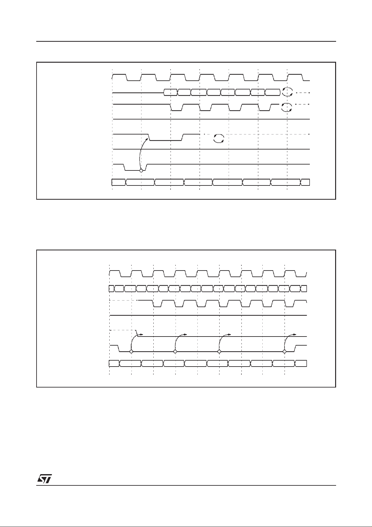
Figure 8. 2X Read data, no delay
1234567
PCICLK
+1
PCIAD[31:0]
AGPADSTBx
AGPRBF#
PCITRDY#
PCIREQ#
PCIGNT#
R1 +5 +6 +7+2 +3 +4
AGPST[2:0]
00x xxx xxx xxx xxxxxx xxx
Figure 8shows 32 bytes being transferred during 4 clocks(compared with 16bytes inAGP 1x mode). The
control signals are identical. The AGPAD_STBx signal has been added when data is transferred at 8
bytes per PCICLK period. AGPAD_STBx represents AGPAD_STB0 and AGPAD_STB1 and are used
by the2X interface logicto indicatewhen valid data ispresenton theAD bus.Thecontrol logic (PCITRDY#
in this case) indicates when data can be used by the target.
Figure 9. 2X Back to back read data, no delay
123456789
PCICLK
+1
PCIAD[31:0]
AGPADSTBx
AGPRBF#
PCITRDY#
PCIGNT#
L6 +1 H5 +1
H4 +1 +L7 L8 +1 H6 +1 L9 +1
AGPST[2:0]
000 001 000 001 000xx 001 000 001
xx
Figure 9 showsback to back 8 byteread transactions. AGPST[2:0]are shown toggling between “000”and
“001” to illustrate thatthey are actually changing. However, theyare not required to change between high
and low priority to do back to back transactions. In this diagram, PCITRDY# is asserted on each clock
since a new transaction starts on each clock.
19/85
Page 20
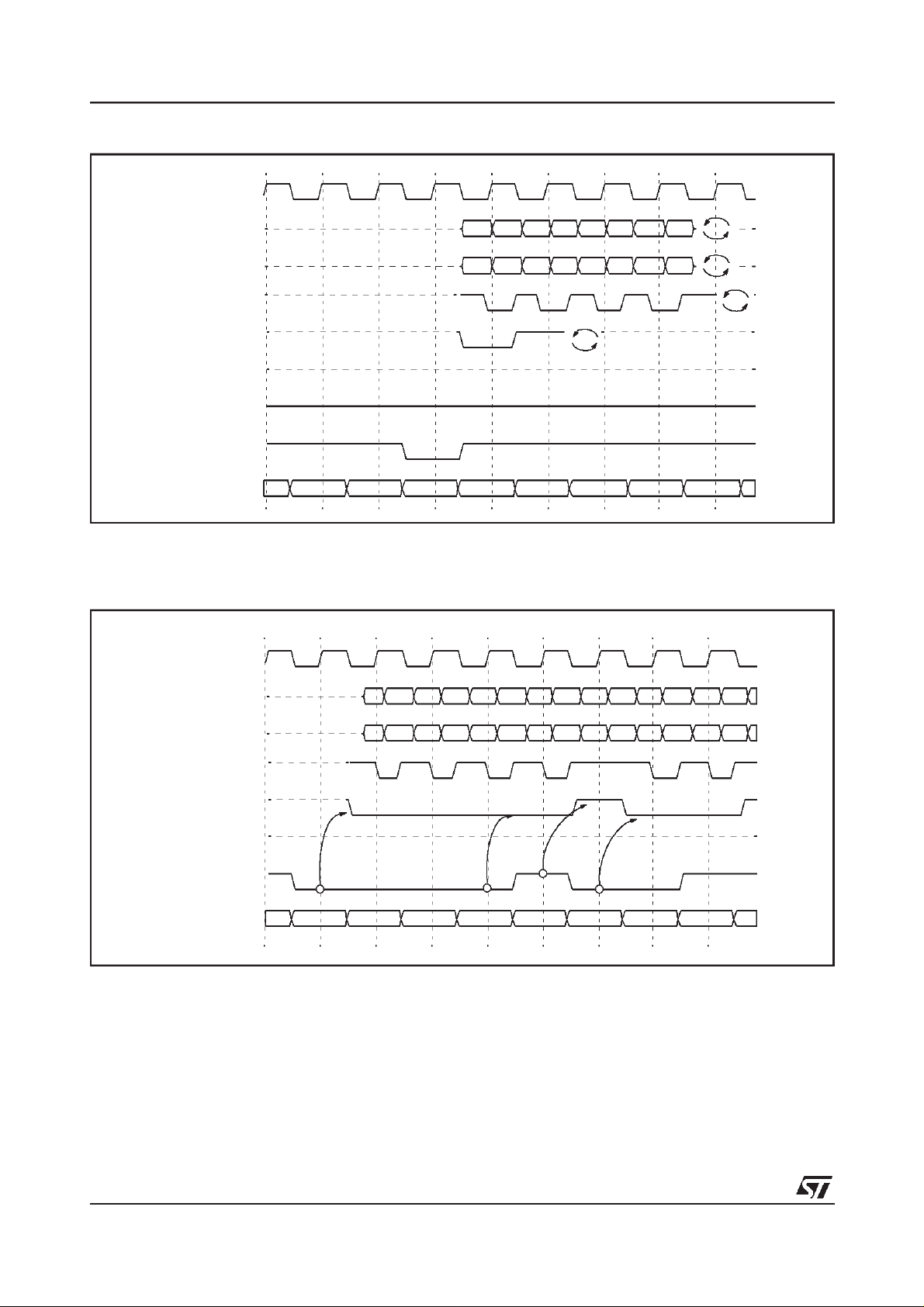
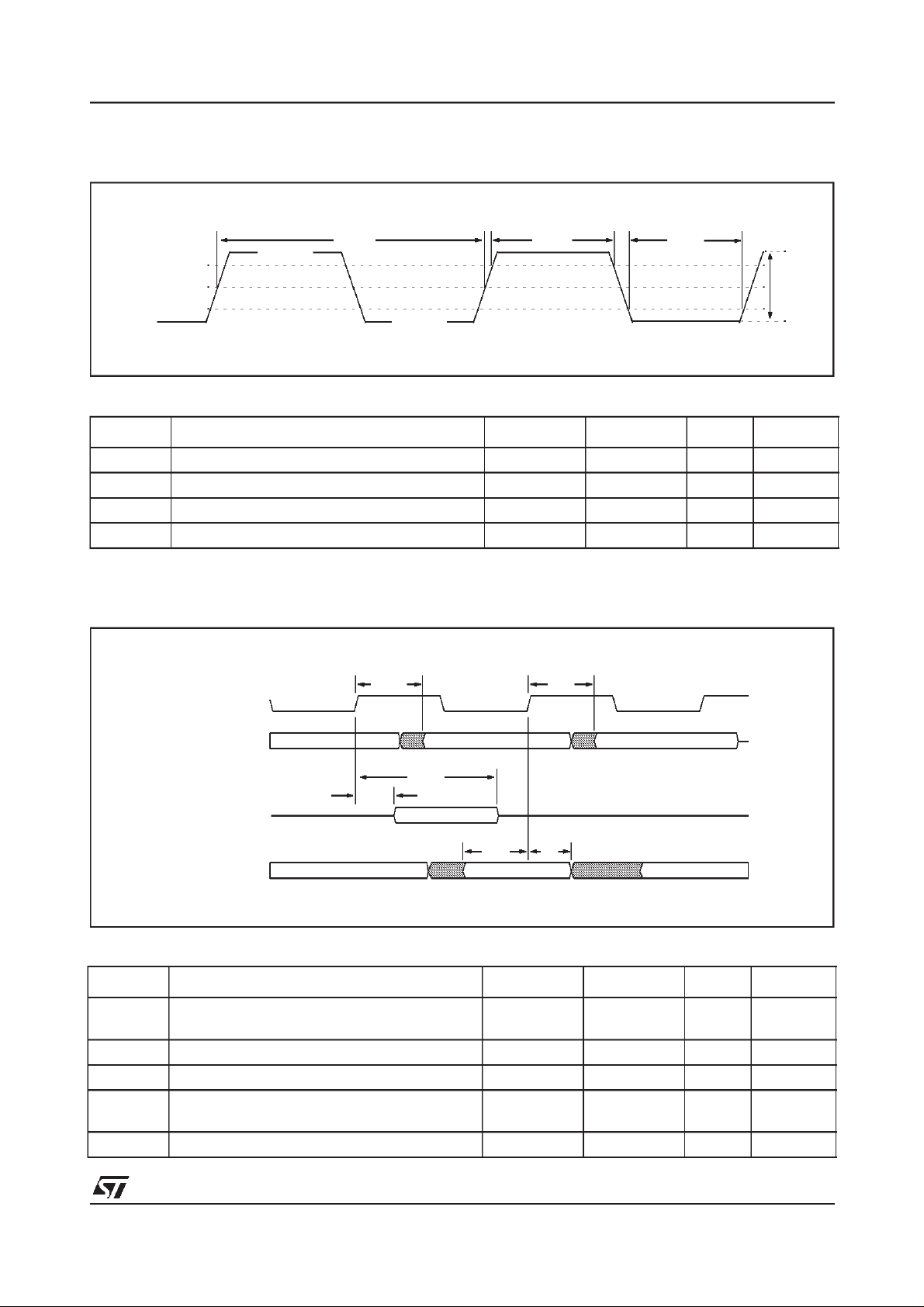
Figure 10. 2X Basic write no delay
123456789
PCICLK
128-BIT 3D MULTIMEDIA ACCELERATORRIVA128ZX
PCIAD[31:0]
PCICBE#
AGPADSTBx
PCIIRDY#
PCITRDY#
PCIREQ#
PCIGNT#
AGPST[2:0]
xxx xxx 01x xxx xxxxx xxx xxx xxx
+2 +3 +4W1 +1 +5 +6 +7
BE BE BEBE BE BE BE BE
Figure 10is a basic write transaction thattransfers data at the2X rate. There is no difference in the control
signals from AGP 1x mode - only more data is moved. The normal control signals determine when data is
valid.
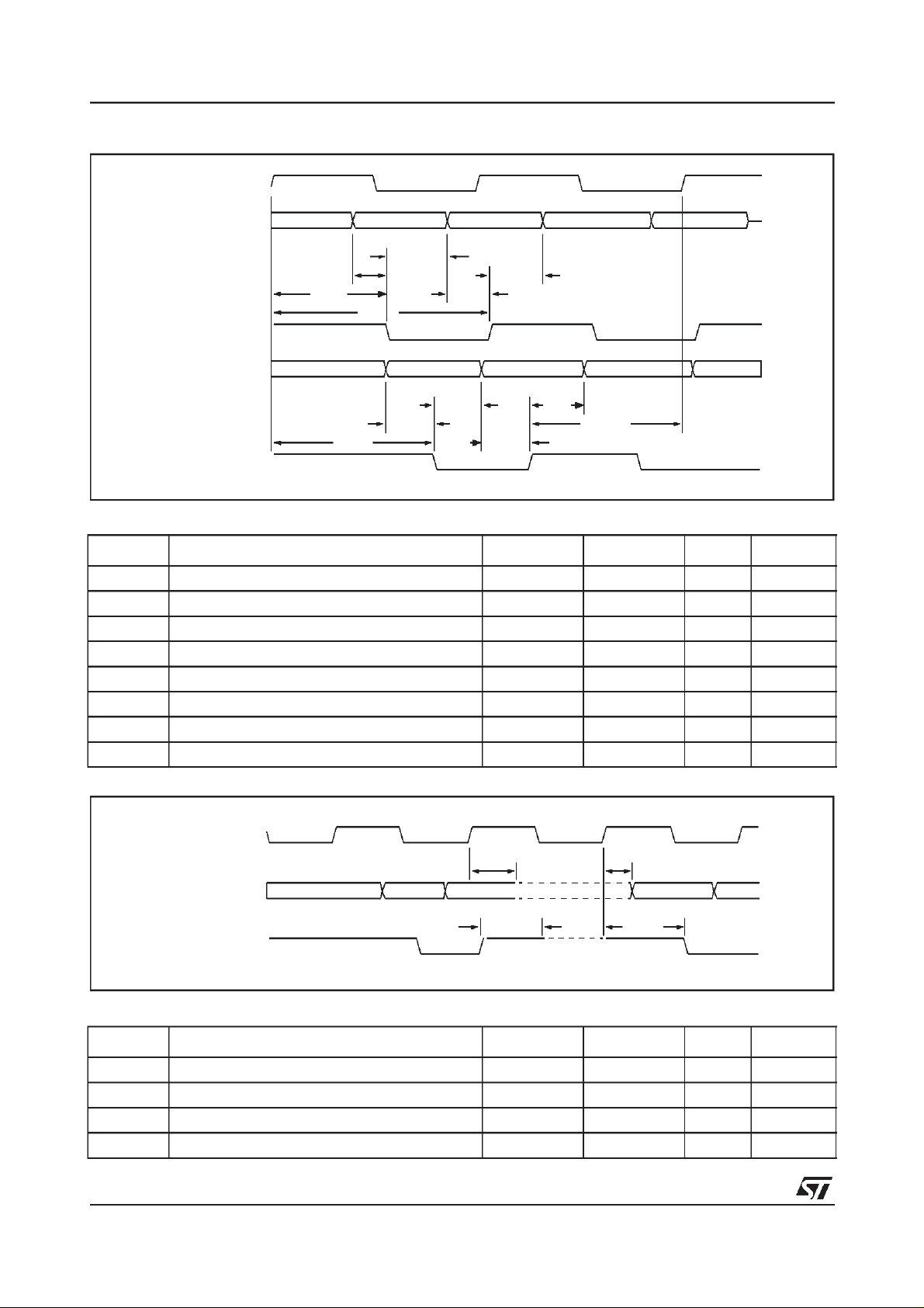
Figure 11. QuadWord writes back to back - no delays
123456789
PCICLK
PCIAD[31:0
PCICBE#
AGPADSTBx
PCIIRDY#
PCITRDY#
PCIGNT#
AGPST[2:0]
]
01x 01x 01x 01x xxxxx 01x 01x xxx
W5 +1 W7 +1W3 +1 W4 +1 W8 +1
W6 +1
BE BEBE BE BE BEBE BE BE BE BE BE
x
Figure 11 illustratesmultiple 8 bytewrite operationscompared with thesingle transfer shownin Figure 10.
When the transactions are short, thearbiter is required to give grants onevery clock or the AD bus willnot
be totally utilized.In this examplea new writeis started on eachrising clock edgeexcept clock 7,because
the arbiter deasserted PCIGNT# on clock 6. Since a new transaction is started on each CLK, PCIIRDY#
is only deasserted on clock 7.
20/85
Page 21
128-BIT 3D MULTIMEDIA ACCELERATOR RIVA128ZX
AGP timing specification
Figure 12. AGP clock specification
t
0.6VDD
PCICLK
0.5VDD
0.4VDD
0.3VDD
Table 1. AGP clock timing parameters
Symbol Parameter Min. Max. Unit Notes
CYC PCICLK period 15 30 ns
t
HIGH PCICLK high time 6 ns
t
LOW PCICLK low time 6 ns
t
PCICLK slew rate 1.5 4 V/ns 1
CYC tHIGH tLOW
2V p-to-p
(minimum)
0.2VDD
NOTES
1 This rise and fall time is measured across the minimum peak-to-peak range as shown in Figure12.
Figure 13. AGP timing diagram
AGPCLK
Output delay
Tri-state output
Input
tVAL
data1 data2
tOFF
tON
tSU
data1 data2
tVAL
tH
Table 2. AGP timing parameters
Symbol Parameter Min. Max. Unit Notes
VAL AGPCLK to signal valid delay (data and control
t
signals)
ON Float to active delay 2 ns
t
OFF Active to float delay 28 ns
t
SU Input set up time to AGPCLK (data and control
t
signals)
HInput hold time from AGPCLK 0ns
t
211ns
7ns
21/85
Page 22
128-BIT 3D MULTIMEDIA ACCELERATORRIVA128ZX
Figure 14. AGP timing diagram (2X data transfer mode)
AGPCLK
Output data
Data1 Data2 Data3 Data4
tDVA
DVB
tTSF
t
tDVB
tDVA
tTSR
Output strobe
Input data
tRSH
Data1 Data2 Data3 Data4
tDH
tDSU
tDH
tRSSU
tDSU
Input strobe
Table 3. AGP timing parameters (2X data transfer mode)
Symbol Parameter Min. Max. Unit Notes
TSF AGPCLK to transmit strobe falling edge 2 12 ns
t
TSR AGPCLK to transmit strobe rising edge 20 ns
t
DVB Output data validbefore strobe 1.7 ns
t
DVA Output data validafter strobe 1.7 ns
t
RSSU Receiver strobe setup time to AGPCLK 6ns
t
RSH Receiver strobe hold time from AGPCLK 1ns
t
DSU Input data to strobe setup time 1 ns
t
DH Input data to strobe hold time 1 ns
t
Figure 15. AGP Strobe/Data turnaround timing diagram (2X data transfer mode)
AGPCLK
tOFFD tOND
PCIAD[31:0]
OFFS
t
tONS
AGPADSTBx
Table 4. AGP Strobe/Data turnaround timing parameters (2X data transfer mode)
Symbol Parameter Min. Max. Unit Notes
OND Float to active delay -1 9 ns
t
OFFD Active to float delay 1 12 ns
t
ONS Strobe active to strobe falling edge setup 6 10 ns
t
OS Strobe rising edge to strobe float delay 6 10 ns
t
22/85
Page 23
128-BIT 3D MULTIMEDIA ACCELERATOR RIVA128ZX
5 PCI 2.1 LOCAL BUS INTERFACE
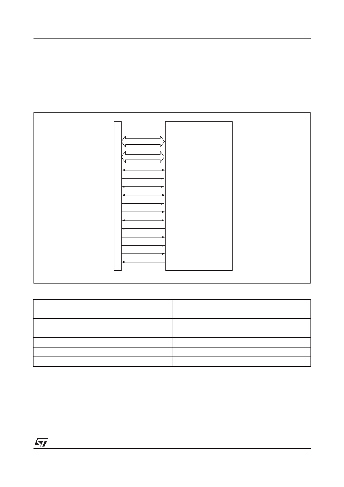
5.1 RIVA128ZX PCI INTERFACE
The RIVA128ZXsupports a gluelessinterface to PCI 2.1 with both master andslave capabilities. Thehost
interface is fully compliant with the 32-bit PCI 2.1 specification.
The Multimedia Accelerator supports PCI bus operation up to 33MHz with zero-wait state capability and
full bus mastering capability handling burst reads and burst writes.
Figure 16. PCI interface pin connections
PCIAD[31:0]
32
PCICBE[3:0]#
4
PCIFRAME#
PCIDEVSEL#
PCIIRDY#
PCI bus
PCITRDY#
PCISTOP#
PCIIDSEL
PCIPAR
PCIREQ#
PCIGNT#
PCICLK
PCIRST#
PCIINTA#
RIVA128ZX
Table 5. PCI bus commands supported by the RIVA128ZX
Bus master Bus slave
Memory read and write Memory read and write
Memory read line I/O read and write
Memory read multiple Configuration read and write
Memory read line
Memory read multiple
Memory write invalidate
23/85
Page 24
128-BIT 3D MULTIMEDIA ACCELERATORRIVA128ZX
5.2 PCI TIMING SPECIFICATION
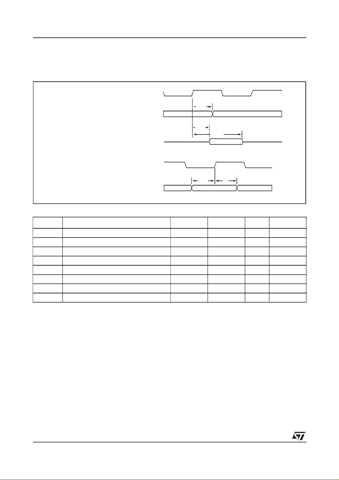
The timing specification of the PCIinterface takes the form of generic setup, hold and delay times of tran-
sitions to and from the rising edge of PCICLK as shown in Figure 17.
Figure 17. PCI timing parameters
PCICLK
VAL
t
Output timing parameters
Output delay
tON
tOFF
Tri-state output
PCICLK
Input timing parameters
tSU tH
Input
Table 6. PCI timing parameters
Symbol Parameter Min. Max. Unit Notes
VAL PCICLK to signal valid delay (bussed signals) 2 11 ns 1
t
(PTP)
VAL
t
ON Float to activedelay 2 ns
t
OFF Active to float delay 28 ns
t
SU Inputset up time to PCICLK (bussed signals) 7 ns 1
t
(PTP)
SU
t
(PTP)
SU
t
H Input hold time fromPCICLK 0ns
t
NOTE
PCICLK to signal valid delay (point to point) 2 12 ns 1
Input set up time to PCICLK (PCIGNT#)10 ns1
Input set up time to PCICLK (PCIREQ#)12 ns
1 PCIREQ# and PCIGNT# are point to point signals andhave different valid delay and input setup times than bussed sig-
nals. All other signals are bussed.
24/85
Page 25
128-BIT 3D MULTIMEDIA ACCELERATOR RIVA128ZX
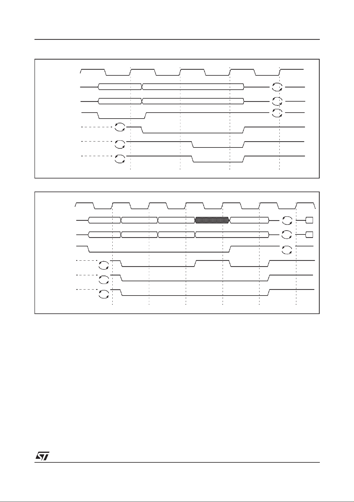
Figure 18. PCI Target write - Slave Write (single 32-bit with 1-cycle DEVSEL# response)
PCICLK
PCIAD[31:0]
PCICBE[3:0]#
PCIFRAME#
PCIIRDY#
PCITRDY#
PCIDEVSEL#
address data
bus cmd BE[3:0]#
(med)
Figure 19. PCI Target write - Slave Write (multiple 32-bit with zero wait state DEVSEL# response)
PCICLK
PCIAD[31:0]
PCICBE[3:0]#
PCIFRAME#
address data0
bus cmd BE[3:0]#
data1 data2
BE[3:0]# BE[3:0]#
PCIIRDY#
PCITRDY#
PCIDEVSEL#
25/85
Page 26
128-BIT 3D MULTIMEDIA ACCELERATORRIVA128ZX
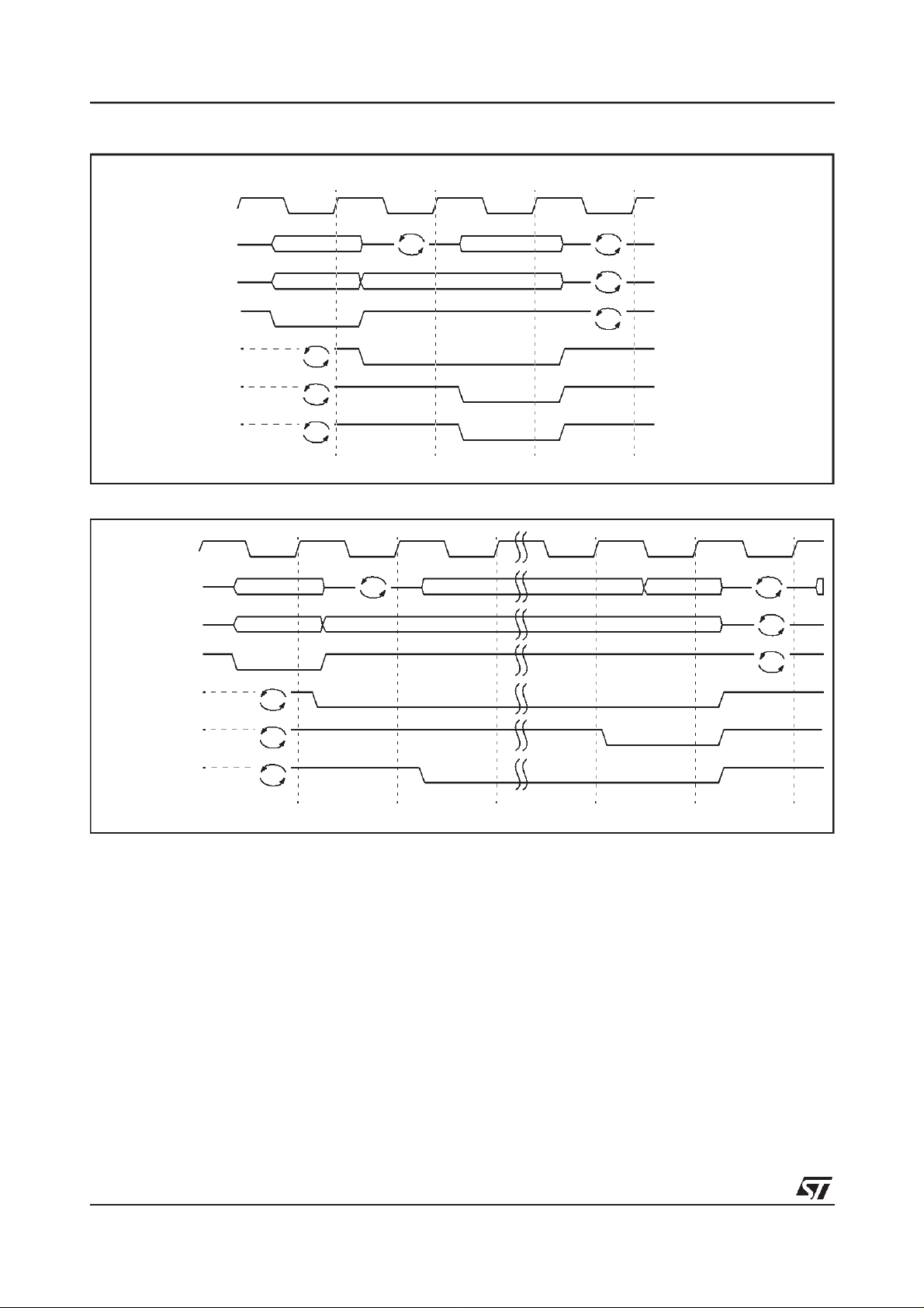
Figure 20. PCI Target read - Slave Read (1-cycle single word read)
PCICLK
PCIAD[31:0]
PCICBE[3:0]#
PCIFRAME#
PCIIRDY#
PCITRDY#
PCIDEVSEL#
address
bus cmd BE[3:0]#
data0
Figure 21. PCI Target read - Slave Read (slow single word read)
PCICLK
PCIAD[31:0]
PCICBE[3:0]#
PCIFRAME#
address
bus cmd BE[3:0]#
data0
PCIIRDY#
PCITRDY#
PCIDEVSEL#
26/85
Page 27
128-BIT 3D MULTIMEDIA ACCELERATOR RIVA128ZX
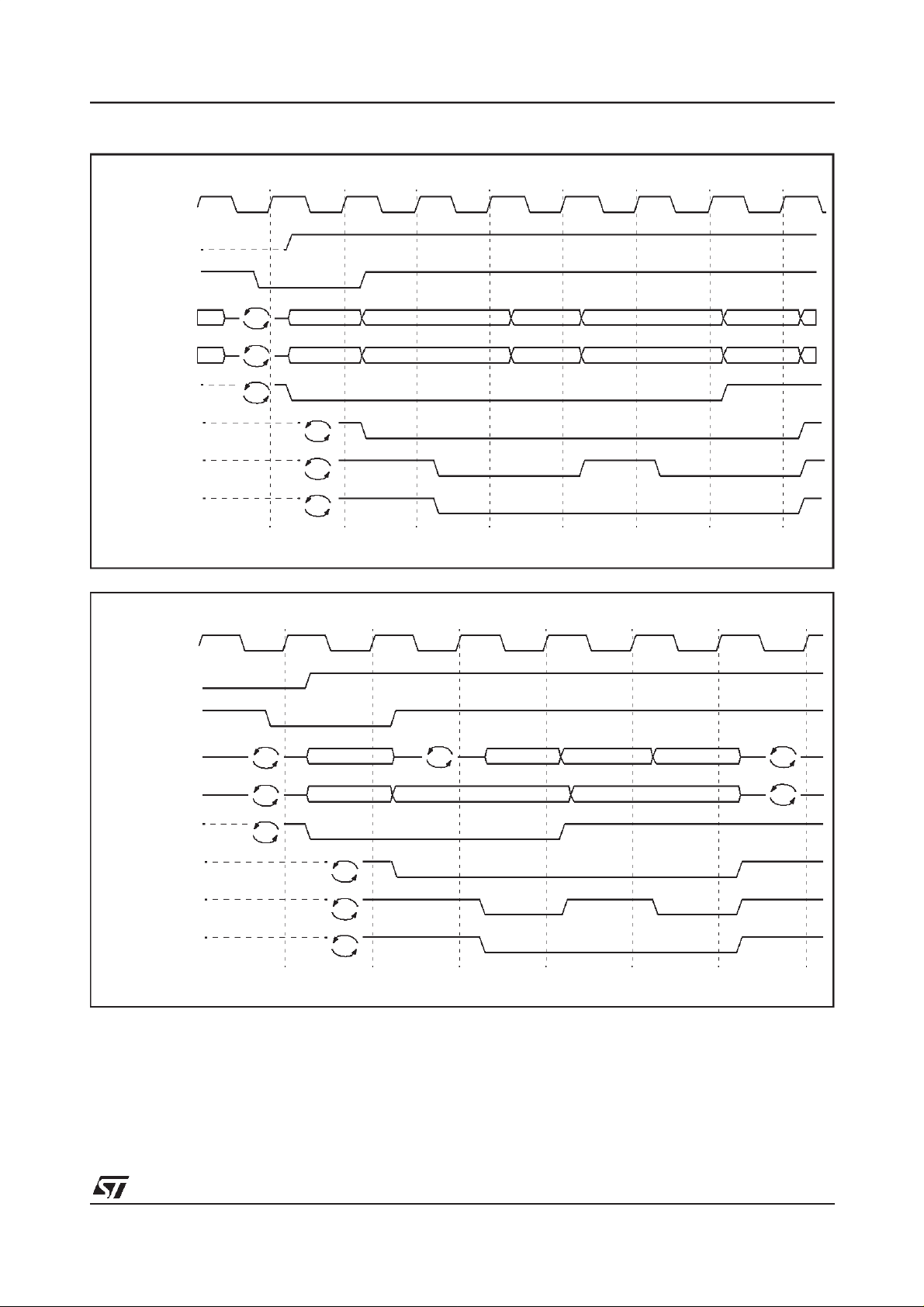
Figure 22. PCI Master write - multiple word
PCICLK
PCIREQ#
PCIGNT#
PCIAD[31:0]
PCICBE[3:0]#
PCIFRAME#
PCIIRDY#
PCITRDY#
PCIDEVSEL#
bus cmd
data0 data1address data2 data3
BE[3:0]# BE[3:0]# BE[3:0]# BE[3:0]#
Figure 23. PCI Master read - multiple word
PCICLK
PCIREQ#
PCIGNT#
PCIAD[31:0]
data0address data1
PCICBE[3:0]#
PCIFRAME#
PCIIRDY#
PCITRDY#
PCIDEVSEL#
Note: The RIVA128ZX doesnot generate fast back to back cycles asa bus master
bus cmd
BE[3:0]# BE[3:0]#
27/85
Page 28
128-BIT 3D MULTIMEDIA ACCELERATORRIVA128ZX
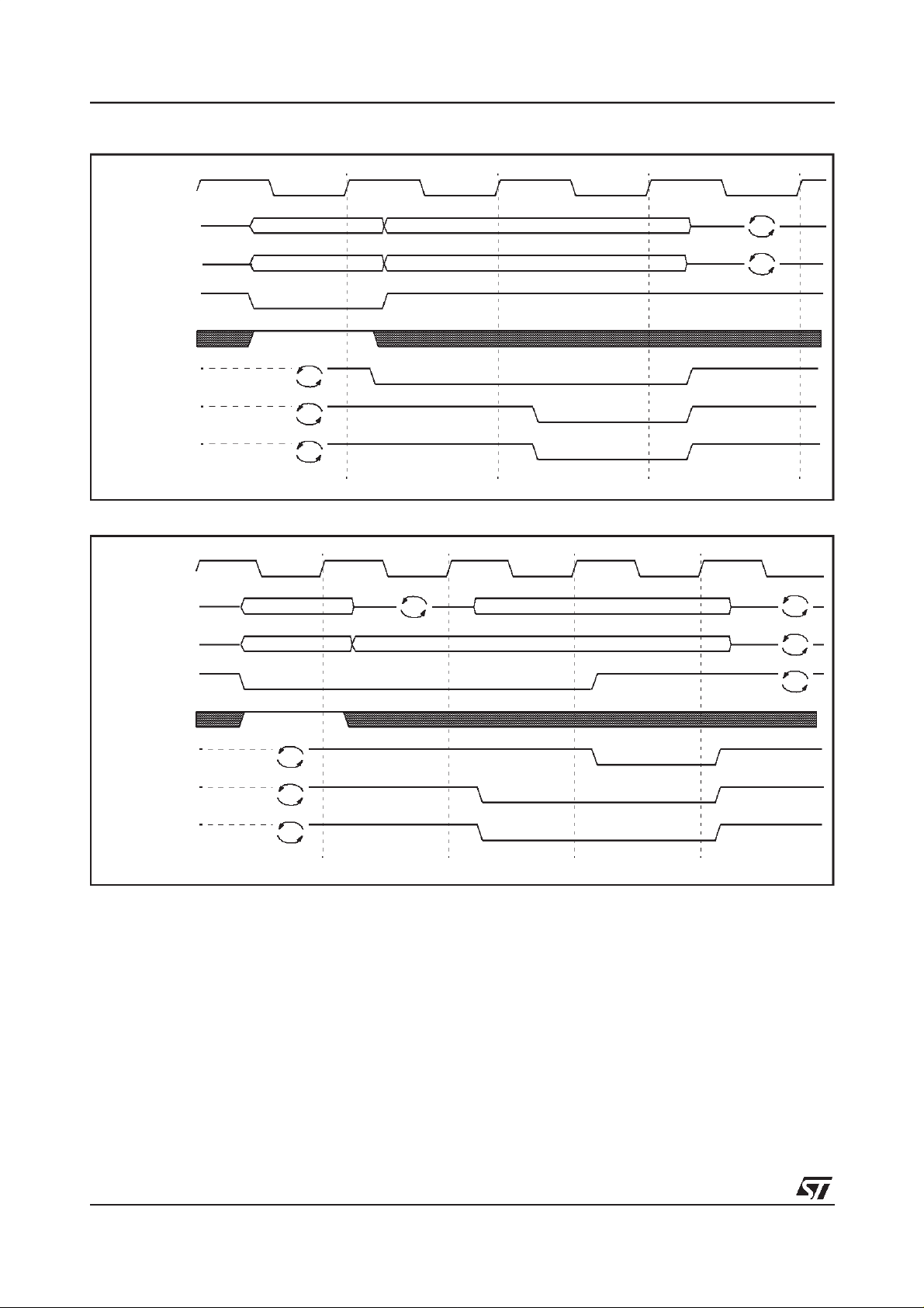
Figure 24. PCI Target configuration cycle - Slave Configuration Write
PCICLK
AD[31:0]
PCICBE[3:0]#
PCIFRAME#
PCIIDSEL
PCIIRDY#
PCITRDY#
PCIDEVSEL#
bus cmd BE[3:0]#
data0address
(med)
Figure 25. PCI Target configuration cycle - Slave Configuration Read
PCICLK
PCIAD[31:0]
PCICBE[3:0]#
bus cmd BE[3:0]#
config_dataaddress
PCIFRAME#
PCIIDSEL
PCIIRDY#
PCITRDY#
PCIDEVSEL#
(med)
28/85
Page 29
128-BIT 3D MULTIMEDIA ACCELERATOR RIVA128ZX
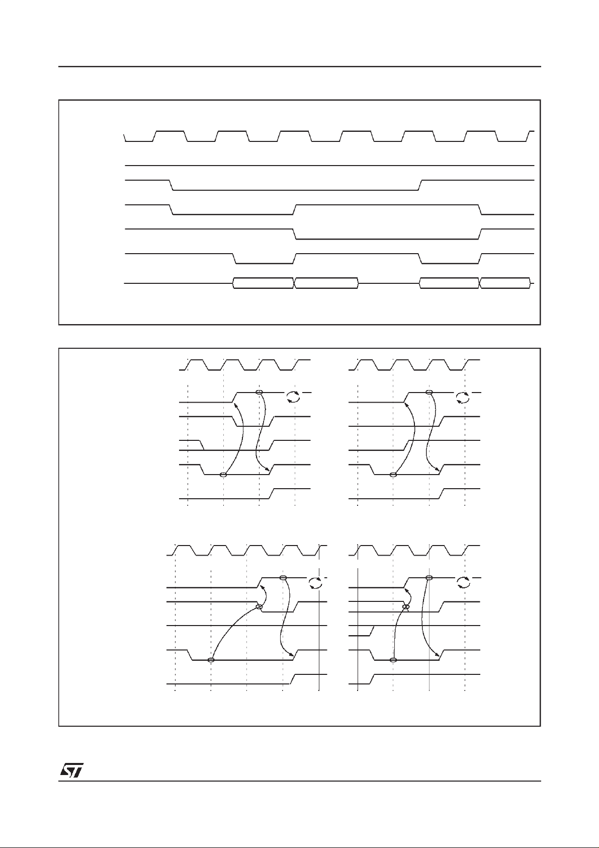
Figure 26. PCI basic arbitration cycle
PCICLK
PCIREQ#_a
PCIREQ#_b
PCIGNT#_a
PCIGNT#_b
PCIFRAME#
PCIAD[31:0]
Figure 27. Target initiated termination
PCICLK
PCIFRAME#
PCIIRDY#
PCITRDY#
PCISTOP#
PCIDEVSEL#
Disconnect - A Disconnect - B
PCICLK
address data address data
access A access B
12341234
123412345
PCIFRAME#
PCIIRDY#
PCITRDY#
PCIPCISTOP#
PCIDEVSEL#
Disconnect -C /Retry Target- Abort
29/85
Page 30

128-BIT 3D MULTIMEDIA ACCELERATORRIVA128ZX
6 FRAMEBUFFER INTERFACE
The RIVA128ZX framebuffer interface supports SDRAM and SGRAM memory. Using SDRAM it can be
configured with an 8MByte 64-bit data bus. With SGRAM it can be configured with a 2 or 4MByte 64-bit
data bus or a 4 or 8MByte 128-bit data bus. The memory configurations supported by RIVA128ZX are
shown in Table 7. All of the framebuffer signalling environment is 3.3V.
Table 7. RIVA128ZX memory configurations
8Mbit
2 internal bank
SGRAM
2MByte 2 devices
64-bit
4MByte 4 devices
128-bit
8MByte 2 banks of 4 devices
128-bit
16Mbit
2 internal bank
SGRAM
N/A N/A N/A
2 devices
64-bit
4 devices
128-bit
16Mbit
4 internal bank
SGRAM
2 devices
64-bit
4 devices
128-bit
16Mbit
1M x 16
SDRAM
N/A
4 devices
64-bit
30/85
Page 31
128-BIT 3D MULTIMEDIA ACCELERATOR RIVA128ZX
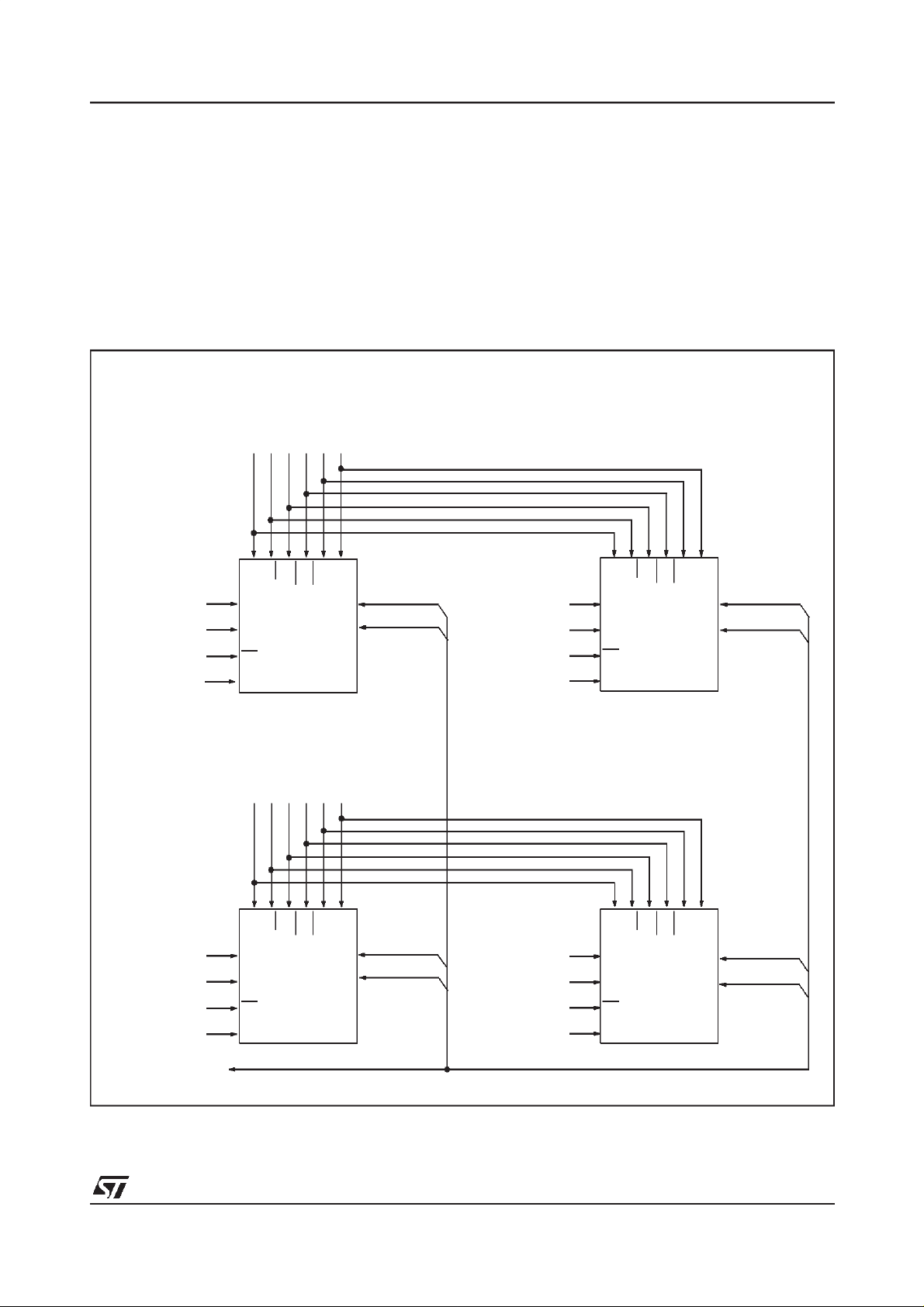
6.1 SDRAM INTERFACE
Two extra address lines are requiredto support 8MByte SDRAM compared with those needed for 4MByte
SGRAM on RIVA 128. These are the A10 signal which was defined on the RIVA 128 pinout for future expansion and the SDRAM’s internal bank select address bit (BA signal). To provide this extra signal the
RIVA128ZX FBCS[1]# pin is internally redefined to be theSDRAM BA/A11 signal.
Since the RIVA128ZX supports a maximum addressable memoryof 8MBytes, SDRAM supportis only allowed with a64-bit databus. Figure28 shows an exampleSDRAMmemory configuration forRIVA128ZX.
Note this figure attempts to scramblethe bytesand data bits within bytes to simplify boardlayout, but this
will depend on how the board components are placed in the layout.
Figure 28. 8MByte SDRAM configuration using 16Mbit devices
FBA[10:0]
FBCS[1]#
FBCKE#
FBRAS#
FBCAS#
FBWE#
FBDQM[3]#
FBDQM[0]#
FBCS[0]#
FBCLK0
FBDQM[5]#
FBDQM[6]#
FBCS[0]#
FBCLK1
WE
CKE
DQML
DQMH
CS
CLK
FBCKE#
FBWE#
WE
CKE
DQML
DQMH
CS
CLK
A[10:0]
RAS
CAS
1M×16
SDRAM
FBA[10:0]
FBRAS#
FBCAS#
A[10:0]
RAS
CAS
1M×16
SDRAM
BA
FBD[31:24]
FBD[7:0]
FBCS[1]#
BA
FBD[47:40]
FBD[55:48]
FBDQM[1]#
FBDQM[2]#
FBCS[0]#
FBCLK0
FBDQM[4]#
FBDQM[7]#
FBCS[0]#
FBCLK1
CKE
DQML
DQMH
CS
CLK
CKE
DQML
DQMH
CS
CLK
WE
WE
A[10:0]
RAS
CAS
1M×16
SDRAM
A[10:0]
RAS
CAS
1M×16
SDRAM
BA
FBD[15:8]
FBD[23:16]
BA
FBD[32:39]
FBD[56:63]
FBD[127:0]
31/85
Page 32
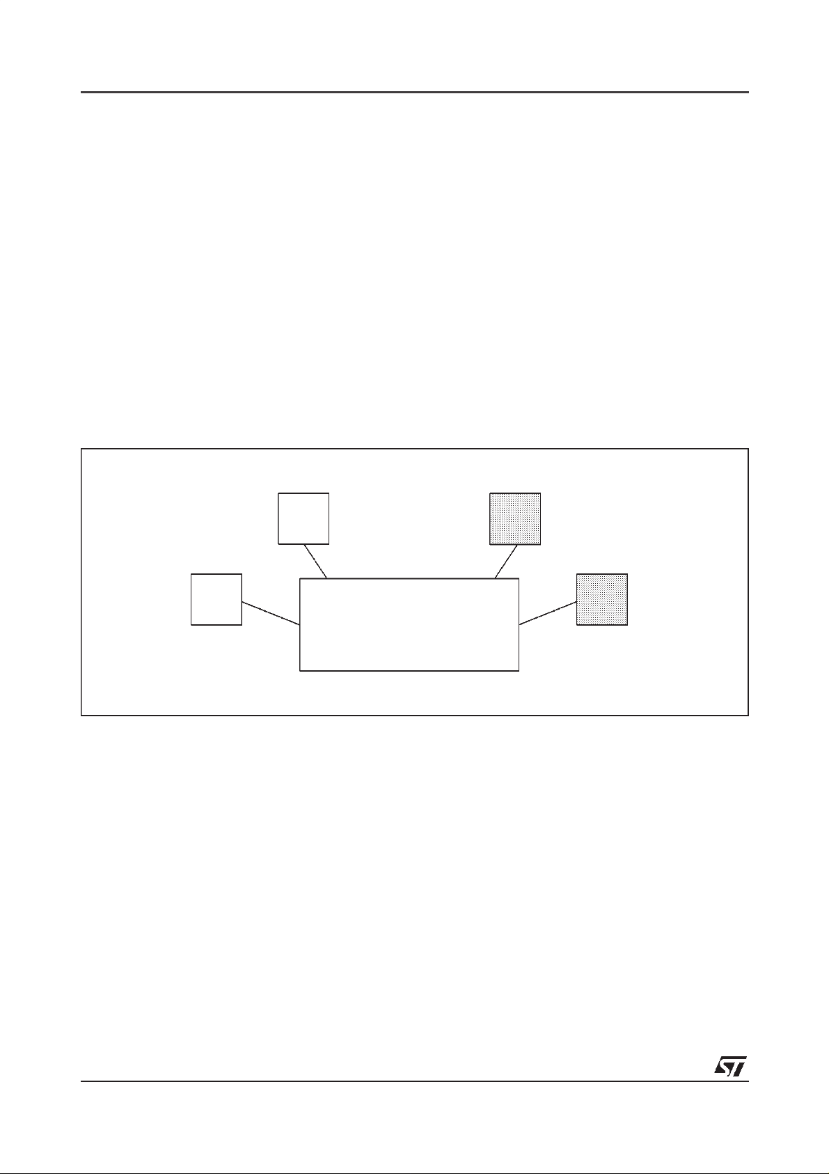
128-BIT 3D MULTIMEDIA ACCELERATORRIVA128ZX
6.2 SGRAM INTERFACE
Signal changes between RIVA 128 and RIVA128ZX
The extraaddress signal (FBA[10])required to address 16MbitSGRAM deviceswas definedonRIVA 128
and was connected to pin 30 of the SGRAM in the RIVA 128 Reference Design schematics. This pin is a
N/C on8Mbit memory devices and itwas also N/C on RIVA 128. For8MByte designsusing 8Mbit devices;
FBCS0# drives the chip selects for the first external bank of memory and FBCS1# drives the second external bank.
The ROMBIOS implementscode which automaticallydetects the configuration and memorytype. Ifa mixture of 4-internalbank and 2-internal bank16Mbit devices are used (e.g. 2soldered down and 2added by
an end user as an SO-DIMM) then RIVA128ZX will program those devices and operateitself as 2-internal
bank. Thereis no supportfor mixed 16Mbit and8Mbit memories(i.e. thereis no6MBytemode) nor is there
support for 16MByte using eight 16Mbit devices. The upgrade path from two devices to four devices has
also been changed to better accommodate board layout for SO-DIMMs. As shown in Figure 29, the first
two memories installed are on the left side of the chip and the upgrade is on the right hand side. This is
different to RIVA 128 which populated the top two chips first and thenpopulated the lower (far left and far
right) memories asthe upgrade. Both forms of 64-bit busare supported in RIVA128ZX and thedata paths
populated are determined by the BIOS during its boot memory detection sequence.
Figure 29. Upgrade from 64-bit 4MByte to 128-bit 8MByte SGRAM via SO-DIMM
First two
memories
installed
Bank 2
512K
x32
Bank 0
512K
x32
FBD[31:0]
FBD[95:64]
RIVA128ZX
Bank 1
512K
FBD[63:32]
FBD[127:96]
x32
Upgrade to
8MByte via
SO-DIMM
Bank 3
512K
x32
32/85
Page 33
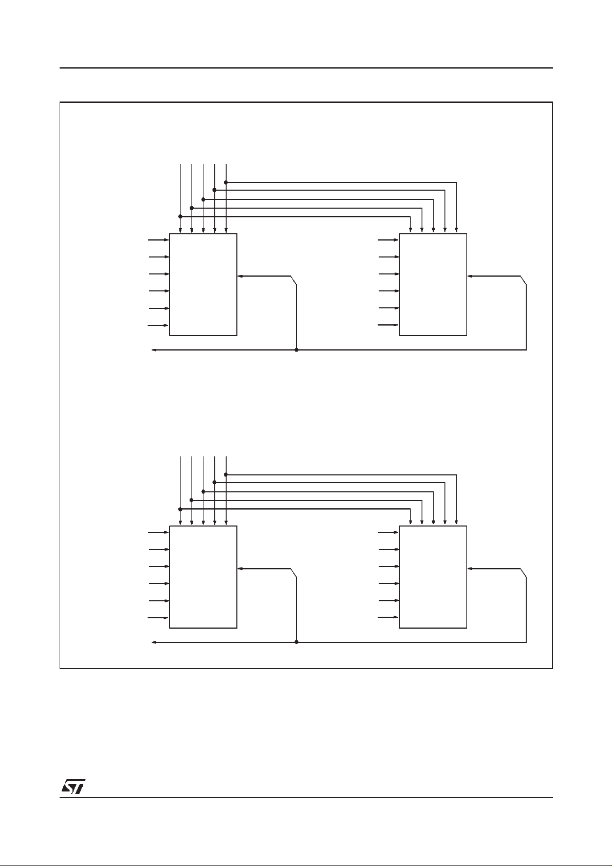
128-BIT 3D MULTIMEDIA ACCELERATOR RIVA128ZX
Figure 30. 4 MByte SGRAM configurations using 16Mbit devices
FBA[10:0]
FBCAS#
FBWE#
FBRAS#
a. RIVA 128 layout compatible
FBCKE#
FBDQM[0]#
FBDQM[1]#
FBDQM[2]#
FBDQM[3]#
FBCS[0]#
FBCLK0
FBD[127:0]
FBDQM[0]#
FBDQM[1]#
FBDQM[2]#
FBDQM[3]#
FBCS[0]#
FBCLK0
Bank 0
512K×32
SGRAM
FBCKE#
FBCAS#
FBWE#
Bank 0
512K×32
SGRAM
FBA[10:0]
FBRAS#
FBDQM[4]#
FBDQM[5]#
FBD[31:0] FBD[63:32]
b. Compatible with RIVA128ZX layout
implementing SO-DIMM upgrade to 8Mbytes
FBD[31:0] FBD[95:64]
FBDQM[6]#
FBDQM[7]#
FBCS[0]#
FBCLK1
FBDQM[8]#
FBDQM[9]#
FBDQM[10]#
FBDQM[11]#
FBCS[1]#
FBCLK0
Bank 1
512K×32
SGRAM
Bank 2
512K×32
SGRAM
FBD[127:0]
NOTE
1 The 64-bit bus data paths populated by RIVA128ZX are determined by the BIOS during its boot memory detection se-
quence.
33/85
Page 34
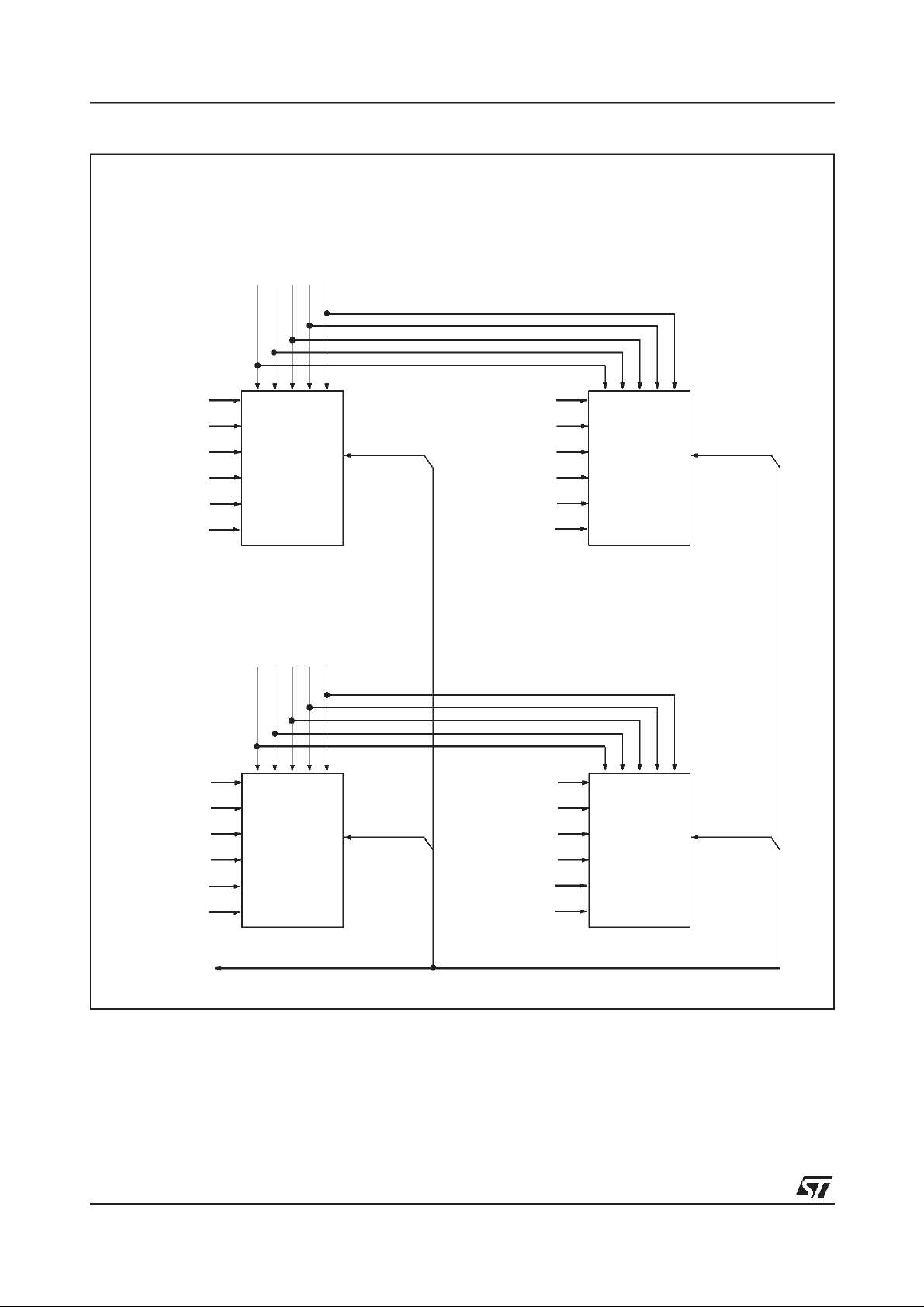
128-BIT 3D MULTIMEDIA ACCELERATORRIVA128ZX
Figure 31. 8MByte SGRAM configuration using 16Mbit devices
FBA[10:0]
FBCKE#
FBRAS#
FBCAS#
FBWE#
FBDQM[0]#
FBDQM[1]#
FBDQM[2]#
FBDQM[3]#
FBCS[0]#
FBCLK0
FBDQM[4]#
FBDQM[5]#
FBDQM[6]#
FBDQM[7]#
FBCS[0]#
FBCLK1
Bank 0
512K×32
SGRAM
FBCKE#
FBCAS#
FBWE#
Bank 1
512K×32
SGRAM
FBA[10:0]
FBRAS#
FBD[63:32]
FBDQM[8]#
FBDQM[9]#
FBD[31:0] FBD[95:64]
FBDQM[10]#
FBDQM[11]#
FBCS[1]#
FBCLK0
FBDQM[12]#
FBDQM[13]#
FBDQM[14]#
FBDQM[15]#
FBCS[1]#
FBCLK1
Bank 2
512K×32
SGRAM
Bank 3
512K×32
SGRAM
FBD[127:96]
34/85
FBD[127:0]
Page 35

128-BIT 3D MULTIMEDIA ACCELERATOR RIVA128ZX
6.3 SDRAM/SGRAM ACCESSES AND COMMANDS
Read and write accesses to SDRAM/SGRAM are burst oriented. SDRAM/SGRAM commands supported
by the RIVA128ZXare shown in Table 9. Initialization of the memory devices is performed in the standard
SDRAM/SGRAM manner. Accesssequences begin with an Active command followed by a Read or Write
command. The address bits registeredcoincident with the Reador Write command are used to select the
starting column location for the burst access. The RIVA128ZX always uses a burst length of one and can
launch anew read or writeon every cycle.
SDRAM/SGRAM has a fully synchronous interface with all signals registered on the positive edge of FB-
CLKx. Multiple clock outputs allow reductions in signal loading and more accuracy in data sampling at
high frequency. The clocksignals can be interspersed as shown inFigure 30, page 33 foroptimal loading
with either 4 or 8MBytes. The I/O timings relative to FBCLKx are shown in Figure 32, page 37.
Table 8. Truth table of supported SDRAM commands
Command
Command inhibit (NOP) H x x x x x x
No operation (NOP) L H H H x x x
Active (select bank and
activate row)
Read (select bank and
column and start read
burst)
Write (select bank and
column and start write
burst)
Precharge (deactivate
row in bank or banks)
Load mode register LLLLxFBCS[1]#,
Write enable/output
enable
Write inhibit/output
High-Z
1
FBCS0# FBRAS# FBCAS# FBWE# FBDQM FBCS[1]#,
FBA[10:0]
LLHHxFBCS[1]#=bank
FBA[10:0]=row
LHLHxFBCS[1]#=bank
FBA[10]=0
FBA[7:0]=col
LHLL xFBCS[1]#=bank
FBA[10]=0
FBA[7:0]=col
LLHLxFBA[10]=code x 3
FBA[10:0] =
opcode
- - - - L - active 2
- - - - H - high-Z 2
FBD[63:0] Notes
valid data
x
x
NOTES
1 FBCKE is high and DSF is low for all supported commands.
2 Activates or deactivates FBD[63:0] during writes (zero clock delay) and reads (two-clock delay).
3 For FBA10 low, FBCS[1]# determines which bank is precharged; for FBA10 high, all banks are precharged irrespective
of the state ofFBCS[1]#.
35/85
Page 36

Table 9. Truth table of supported SGRAM commands
128-BIT 3D MULTIMEDIA ACCELERATORRIVA128ZX
Command
Command inhibit (NOP) H x x x x x x
No operation (NOP) L H H H x x x
Active (select bank and
activate row)
Read (select bank and
column and start read
burst)
Write (select bank and
column and start write
burst)
Precharge (deactivate
row in bank or banks)
Load mode register LLLLxFBA[10:0]=
Write enable/output
enable
Write inhibit/output
High-Z
NOTES
1
1 FBCKE is high and DSF is low for all supported commands.
2 Activates or deactivates FBD[127:0] during writes (zero clock delay) and reads (two-clock delay).
3 For FBA9 low, FBA10 determines which bank isprecharged; for FBA9 high, all banks are precharged irrespectiveof the
state ofFBA10.
FBCS0#,
FBCS1#
FBRAS# FBCAS# FBWE# FBDQM FBA[10:0] FBD[127:0] Notes
LLHHxFBA[10]=bank
FBA[9:0]=row
LHLHxFBA[10]=bank
FBA[9]=0
FBA[7:0]=col
LHLLxFBA[10]=bank
FBA[9]=0
FBA[7:0]=col
LLHLxFBA[10]=code x 3
opcode
- - - - L - active 2
- - - - H - high-Z 2
x
x
valid data
SDRAM/SGRAM Initialization
SDRAM/SGRAMs must be powered-up and initialized in a predefined manner. The first SDRAM/SGRAM
command is registered onthe first clock edge following PCIRST# inactive.
All internal SDRAM/SGRAMbanks are precharged to bring the device(s)into the “all bank idle” state. The
SDRAM/SGRAM mode registers are then programmed and loaded to bring them into a defined state before performing any operational command.
SDRAM/SGRAM Mode register
The Moderegister definesthe mode ofoperation ofthe SDRAM/SGRAM.This includesburst length, burst
type, read latency and SDRAM/SGRAM operating mode.The Mode register is programmed via the Load
Mode register and retains its state until reprogrammed or power-down.
Mode registerbits M[2:0]specifythe burstlength; forthe RIVA128ZXSDRAM/SGRAMinterface thesebits
are set to zero, selecting a burst length of one. In this case FBA[7:0] select the unique column to be accessed and Mode register bit M[3] is ignored. Mode register bits M[6:4] specify the read latency; for the
RIVA128ZX SDRAM/SGRAM interface these bits are set to either 2 or 3, selecting a burst length of 2 or
3 respectively.
36/85
Page 37
128-BIT 3D MULTIMEDIA ACCELERATOR RIVA128ZX
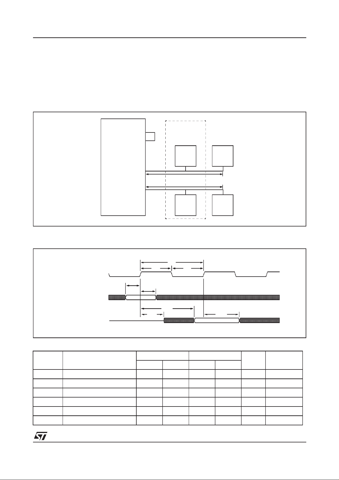
6.4 LAYOUT OF FRAMEBUFFER CLOCK SIGNALS
Separate clock signals FBCLK0 and FBCLK1 are provided for each bank of memory to give reduced
clock skew and loading. Additionally there is a clock feedback loop between FBCLK2 and FBCLKFB.
It is recommended that long traces are used without tunable components. If the layout includes provision
for expansion to 8MBytes, the clock path to the 4MByte parts should be at the end of the trace, and the
clock path to the 8MByte expansion located between the RIVA128ZX and the 4MByte parts as shown in
Figure 32. FBCLK2 and FBCLKFB should be shorted together as close to the package as possible.
Figure 32. Recommended memory clock layout
FBCLK2
FBCLKFB
RIVA128ZX
FBCLK0
FBCLK1
Expansion
to 8MBytes
Bank 1 Bank 0
512K
x32
t
t
512K
x32
6.5 FRAMEBUFFER INTERFACE TIMING SPECIFICATION
Figure 33. SDRAM/SGRAM I/O timing diagram
tCK
FBCLKx
FBA[10:0], FBD[63:0]
CH
t
tAS,tDS
tAH,tDH
tCL
512K
x32
512K
x32
tAC
FBD[63:0]
tLZ
tOH
Table 10. SDRAM/SGRAM I/O timing parameters
Symbol Parameter Min. Max. Unit Notes
-10 -12 -10 -12
tCK CLK period 10 12 - - ns
tCH CLK high time 3.5 4.5 - - ns
tCL CLK low time 3.5 4.5 - - ns
tAS Address setup time 3 4 - ns
tAH Address hold time 1 1 - ns
tDS Write data setup time 3 4 - ns
37/85
Page 38
128-BIT 3D MULTIMEDIA ACCELERATORRIVA128ZX
Symbol Parameter Min. Max. Unit Notes
-10 -12 -10 -12
tDH Write data hold time 1 1 - ns
tOH Read data hold time 3 3 - ns
tAC Read data access time 9 9 - ns
tLZ Data out low impedancetime 0 0 - ns
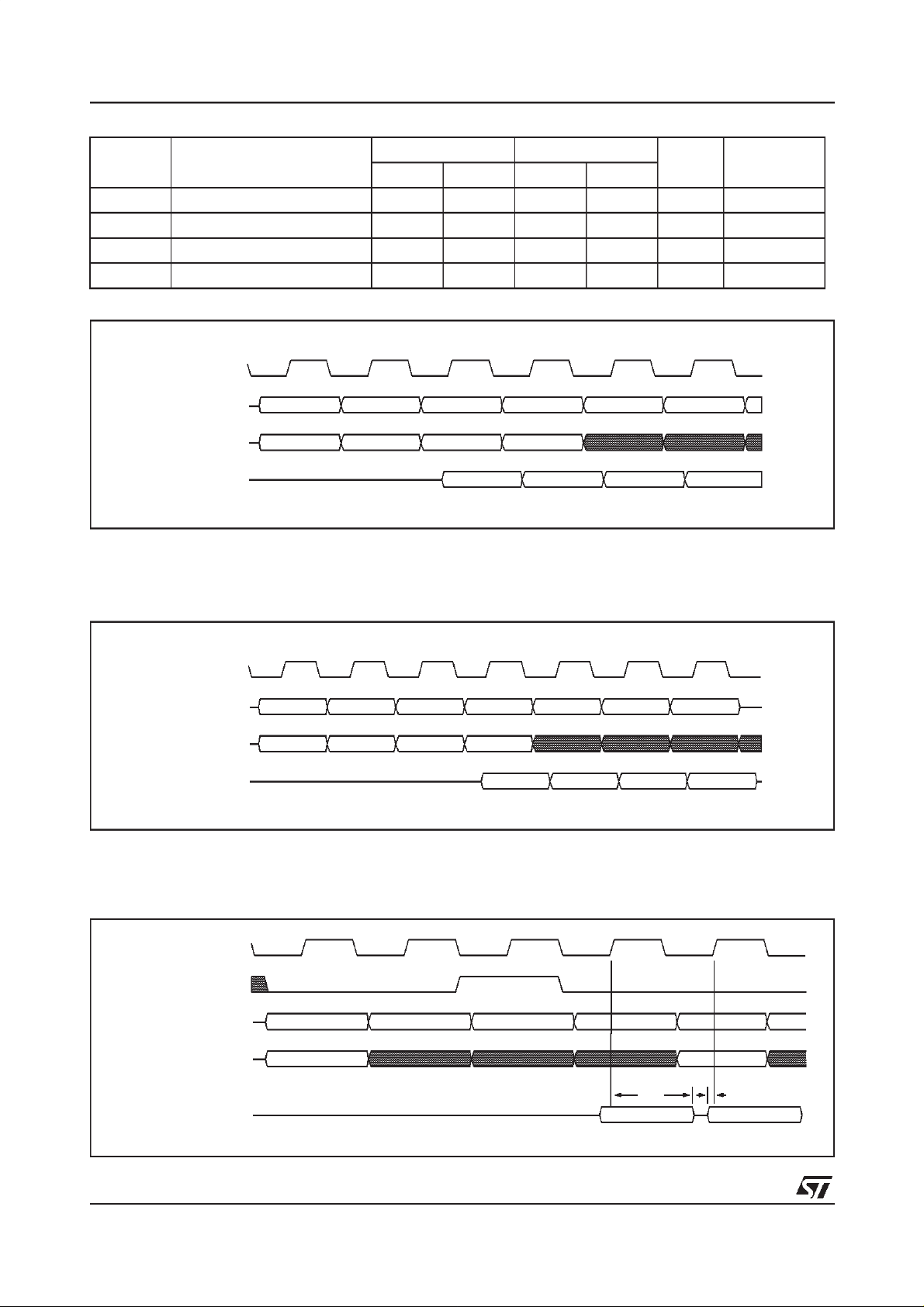
Figure 34. SDRAM/SGRAM random read accesses within a page, read latency of two
FBCLKx
Command
FBA[10:0]
FBD[63:0]
NOTE
1 Covers either successive reads to the active row in a given bank, or to the active rows in different banks. DQMs are all
active (LOW).
read read read
bank, col n bank, col a bank, col x bank, col m
data n data a
read nop nop
data x data m
Figure 35. SDRAM/SGRAM random read accesses within a page, read latency of three
FBCLKx
Command
FBA[10:0]
read read read
bank, coln bank, col a bank, col x bank, col m
read nop nop
1
1
nop
FBD[63:0]
NOTE
1 Covers either successive reads to the active row in a given bank, or to the active rows in different banks. FBDQM is all
active (LOW).
data n
data a data x data m
Figure 36. SDRAM/SGRAM read to write, read latency of three
FBCLKx
TDDQM
Command
FBA[10:0]
read nop nop
bank, col n
nop write
bank, col b
tHZ tDS
FBD[63:0]
38/85
read data n
write data b
Page 39
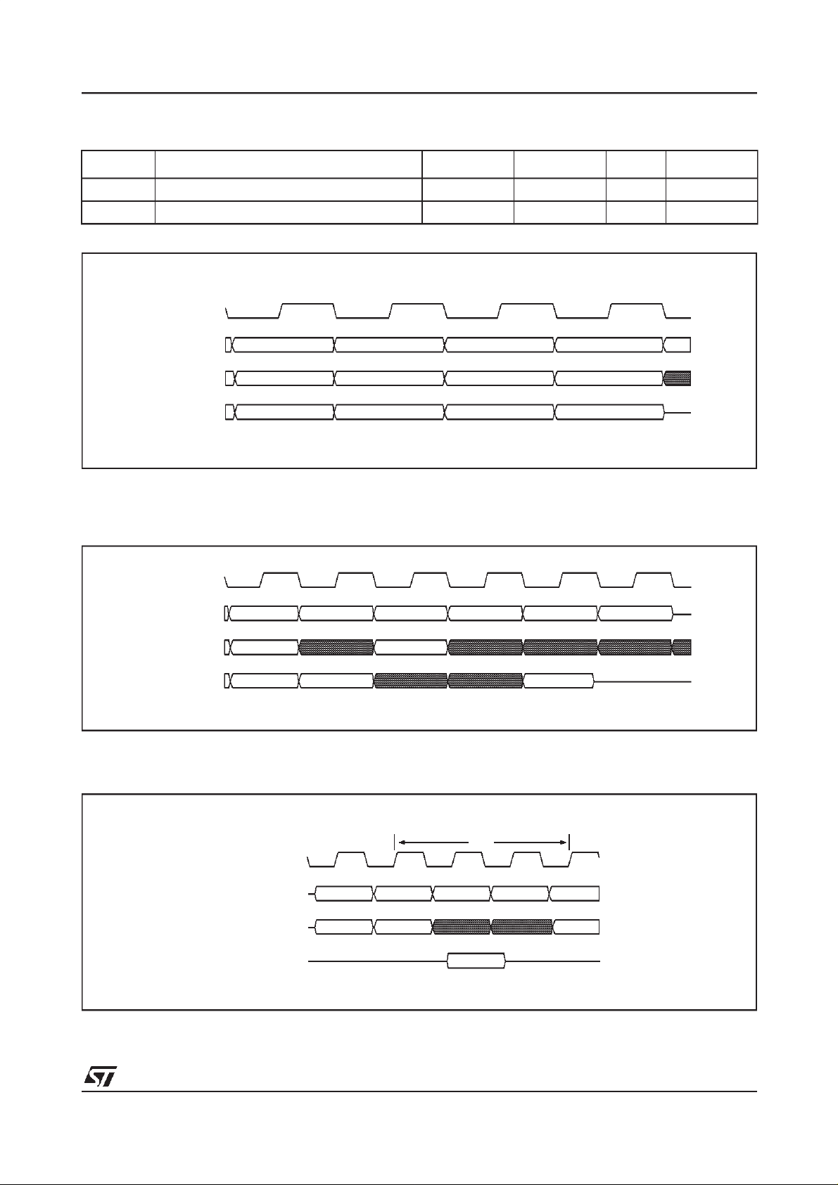
128-BIT 3D MULTIMEDIA ACCELERATOR RIVA128ZX
Table 11. SDRAM/SGRAM I/O timing parameters
Symbol Parameter Min. Max. Unit Notes
tHZ Data out high impedance time 4 10 ns
tDS Write data setup time 4 ns
Figure 37. SDRAM/SGRAM random write cycles within a page
FBCLKx
Command
FBA[10:0]
FBD[63:0]
NOTE
1 Covers eithersuccessive writes to the activerowin a given bank or to the active rows indifferentbanks.FBDQM is active
(low).
write write write write
bank, col n bank, col a bank, col x bank, col m
data n data a data x data m
Figure 38. SDRAM/SGRAM write to read cycle
FBCLKx
Command
FBA[10:0]
FBD[63:0]
NOTE
1 A read latencyof 2is shown for illustration
write nop read nop nop nop
bank,
col n
write
data n
write
data n
bank,
col b
read
data b
Figure 39. SDRAM/SGRAM read to precharge, read latency of two
NOTE
1 FBDQM is active(low)
FBCLKx
Command
FBA[10:0]
FBD[63:0]
read precharge nop
bank, col n
bank(s) bank,row
tRP
nop active
data n
39/85
Page 40
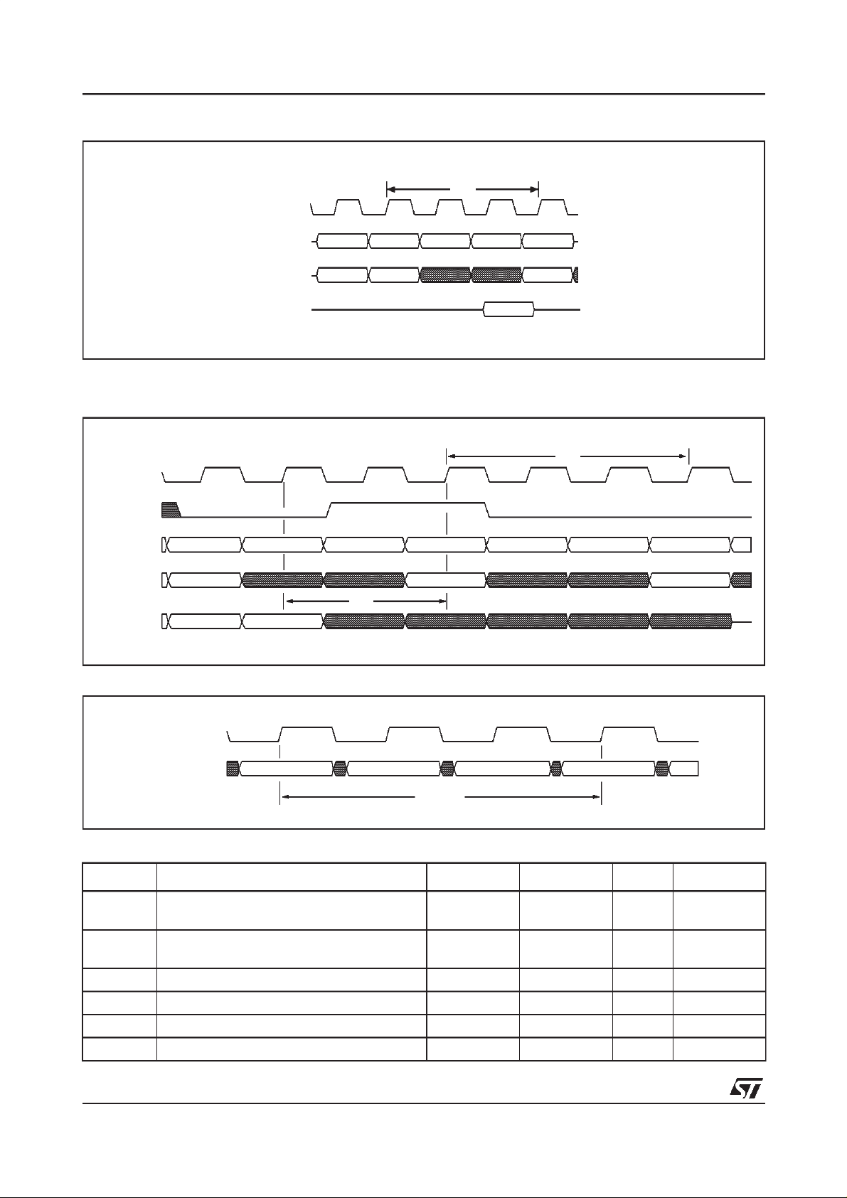
128-BIT 3D MULTIMEDIA ACCELERATORRIVA128ZX
Figure 40. SDRAM/SGRAM read to precharge, read latency of three
FBCLKx
NOTE
1 FBDQM is active(low)
Command
FBA[10:0]
FBD[63:0]
bank,
col n
precharge nop nop active
read
bank(s) bank,
Figure 41. SDRAM/SGRAM Write to Precharge
FBCLKx
FBDQM#
Command
FBA[10:0]
FBD[63:0]
write nop nop precharge nop nop active
bank, col n
tWR
write data n write data
n+1
tRP
row
data n
t
RP
bank(s) row
Figure 42. SDRAM/SGRAM Active to Read or Write
FBCLKx
Command
active nop nop
RCD
t
read or write
Table 12. SDRAM/SGRAM timing parameters
Symbol Parameter Min. Max. Unit Notes
tCS FBCSx, FBRAS#, FBCAS#, FBWE#,
FBDQM setup time
tCH FBCSx, FBRAS#, FBCAS#, FBWE#,
FBDQM hold time
3ns
1ns
tMTC Load Mode register command to command 2 tCK
tRAS Active to Precharge command period 7 tCK
tRC Active to Active command period 10 tCK
tRCD Active to Read or Write delay 3 tCK
40/85
Page 41

128-BIT 3D MULTIMEDIA ACCELERATOR RIVA128ZX
Symbol Parameter Min. Max. Unit Notes
tREF Refresh period(1024 cycles) 16 ms
tRP Precharge command period 4 tCK
tRRD Active bank A to Active bank B command
period
tT Transition time 1 ns
tWR Write recovery time 2 tCK
3tCK
41/85
Page 42
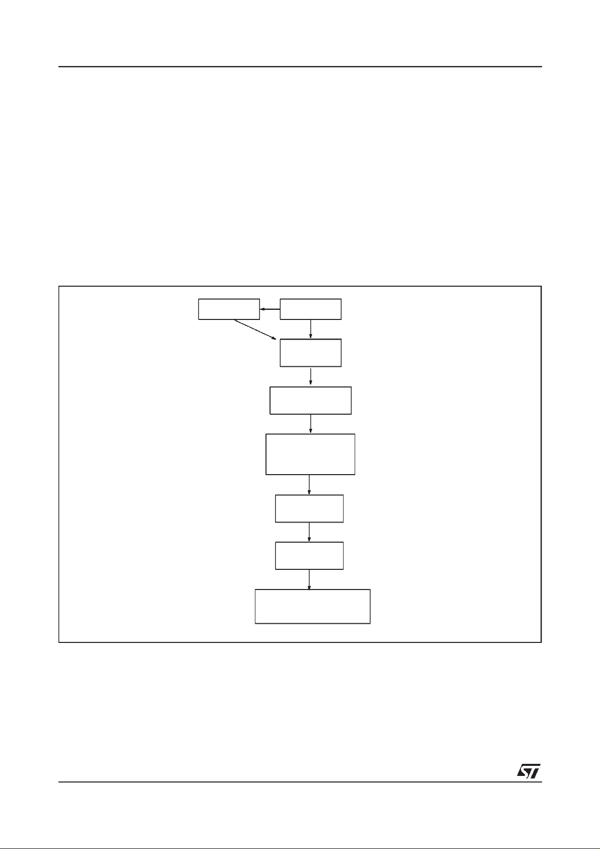
128-BIT 3D MULTIMEDIA ACCELERATORRIVA128ZX
7 VIDEO PLAYBACK ARCHITECTURE
The RIVA128ZX video playback architecture is
designed to allow playback ofCCIR PAL or NTSC
video formats with the highest quality while requiring the smallest video surface. The implementation is optimized around the Windows 95 Direct
Video and ActiveX APIs, and supports the following features:
• Accepts interlaced video fields:
- This allows the off-screen video surface to
consume less memory since only one field
(half of each frame) is stored. Double buffering between fields is done in hardware with
Figure 43. Video scaler pipeline
Linestore
‘temporal averaging’ being applied based on
intraframing.
• Linestore:
- To support high quality video playback the
RIVA128ZX memory controller and video
overlay engine supportshorizontal and vertical interpolationusing a3x2 multitapinterpolating filterwith imagesharpening.
• YUV to RGB conversion:
- YUV 4:2:2 format to 24-bit RGB true-color
- Chrominance optimization/user control
• Color key video composition
YUV
Vertical
Interpolation
Filter
(Smooth/Sharpen)
Color Space
Conversion to 24-bit
RGB
Horizontal
Interpolation
24-bit RGB
Video output
Video windowing,merge
with graphics pixel pipeline
42/85
Page 43

128-BIT 3D MULTIMEDIA ACCELERATOR RIVA128ZX
7.1 VIDEO SCALER PIPELINE
The RIVA128ZX video scaler pipeline performs
stretching of videoimages inany arbitrary factorin
both horizontal and vertical directions. The video
scaler pipeline consists of the following stages:
1 Vertical stretching
2 Filtering
3 Color space conversion
4 Horizontal stretching
Vertical stretching
Vertical stretching is performed on pixels prior to
color conversion. Thevideo scaler linearly interpolates the pixelsin the vertical direction using an internal buffer which stores the previous line of pixel
information.
Filtering
After vertical interpolation, the pixels are horizontally filtered using an edge-enhancement or a
smoothing filter. The edge-enhancement filter enhances picture transition information to prevent
loss of image clarity following the smoothing filtering stage. The smoothing filter is a low-pass filter
that reduces the noise in the source image.
Color space conversion
The video overlay pipeline logic converts images
from YUV 4:2:2 format to 24-bit RGB true-color.
The default color conversion coefficients convert
from YCrCb to gamma corrected RGB.
Saturation controls make sure that the conversion
does not exceed the output range. Four control
flags in thecolor converter provides 16 sets of color conversion coefficients to allow adjustment of
the hue and saturation. The brightness of each
R G B component can also be individually adjusted, similar to the brightness controls of the monitor.
Horizontal stretching
Horizontal stretching is done in 24-bit RGB space
after color conversion. Each component is linearly
interpolated using a triangle 2-tap filter.
Windowing and panning
Video images are clipped to arectangular window
by a pair of registers specifying the position and
width.
By programming the video start address and the
video pitch,the video overlaylogic also supportsa
panning windowthatcan zoominto aportion ofthe
source image.
Video composition
With the color keying feature enabled, a programmable key in the graphics pixel stream allows selection ofeither thevideo orthe graphics outputon
a pixel by pixel basis. Color keying allows any arbitrary portions of the video to overlay the graphics.
With color keying disabled and video overlay
turned on, the video output overlays the graphics
in the video window.
Interlaced video
The video overlay can display both non-interlaced
and interlaced video.
Traditional video overlay hardware typically drops
every other field of an interlaced video stream,
resulting in a low framerate. Some solutions have
attempted to overcome the this problem by deinterlacing the fields into a single frame. This
however introduces motion artifacts. Fast moving
objects appearing in different positions in different
fields, when deinterlaced, introduces visible
artifacts which look like hair-like lines projecting
out of the object.
43/85
Page 44
Figure 44. Displaying 2 fields with 1:1 ratio
Frame 1 (Top field) Frame 2 (Bottom field)
128-BIT 3D MULTIMEDIA ACCELERATORRIVA128ZX
Line 10
Line 11
Interpolated line
(Line 11 & 13)
Line 13
The RIVA128ZX video overlay handles interlaced
video by displaying every field, at the original frame
rate of the video (50Hz for PAL and 60Hz for
NTSC). The video scaling logic upscales
tical direction
,the luma components in each field
,in the ver-
and linearly interpolates successive lines to produce the
ed scale is applied such that
missing linesof eachfield. This interpolat-
the full frame size of
each field is stretched to the desired height.
Interpolated line
(Line 10 & 12)
Line 12
The video scaler offsets the bottom field image by
half a source imageline to ensure that both frames
when played back align vertically.
The vertical filtering results in a smooth high quality
video playback.
ter another
terlaced video output
els ineach fieldare
Alsoby displaying bothfields oneaf-
, anymotion artifacts often foundin dein-
are removed, because the pix-
displayed in theorder in whichthe
original source was captured.
44/85
Page 45
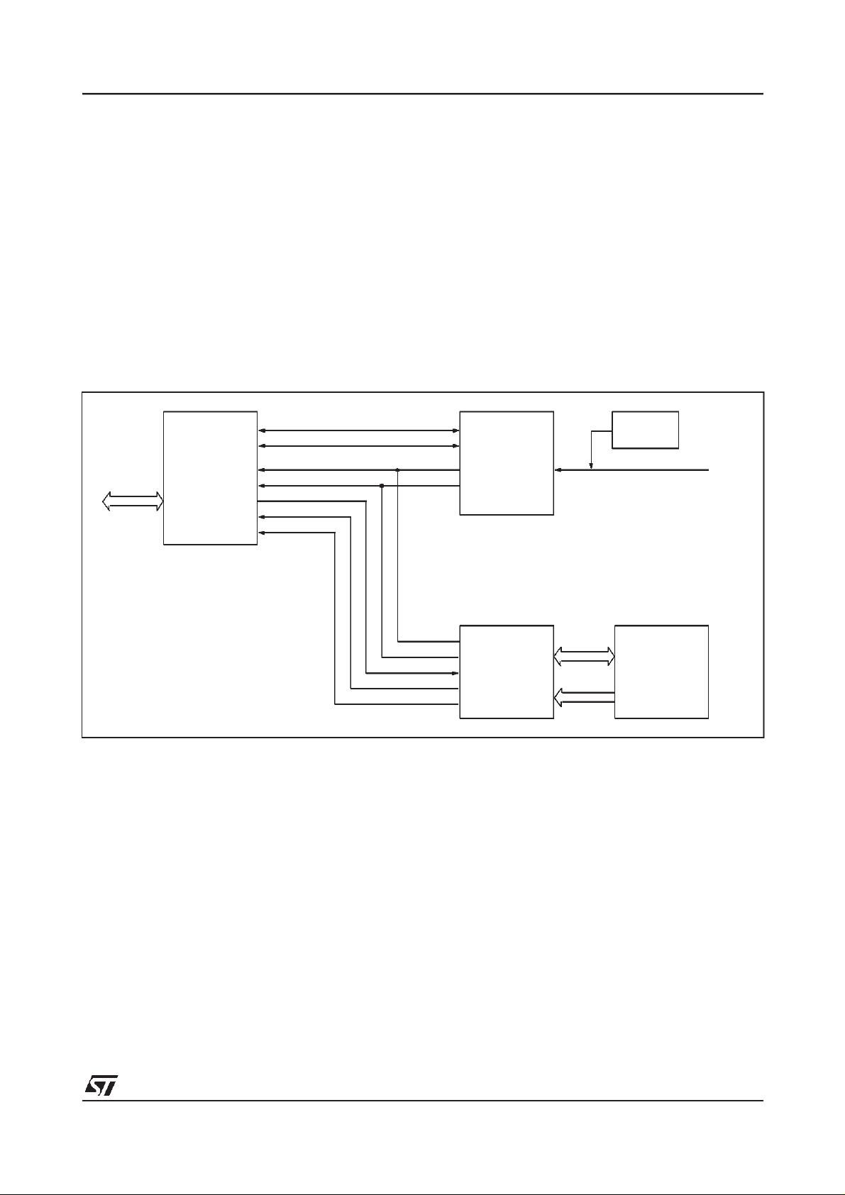
128-BIT 3D MULTIMEDIA ACCELERATOR RIVA128ZX
8 VIDEO PORT
The RIVA128ZXMultimedia Accelerator introduces a multi-function Video Port that has been designed to exploit the bus masteringfunctionality of
the RIVA128ZX. The Video Port is compliant with
a simplified ITU-R-656 videoformat with control of
attached video devices performed through the
RIVA128ZX serialinterface. VideoPort supportincludes:
• Windows 95 DirectMPEG API acceleration by
providing:
- Bus mastered compressed data transfer to
attached DVD and MPEG-2 decoders
Figure 45. Connections to multiple video modules
SDA
SCL
MPCLK
PCI/AGP
RIVA128ZX
MPAD[7:0]
MPFRAME#
MPDTACK#
MPSTOP#
- Local interrupt and pixel stream handling
- Hardware buffer management of compressed data, decompressed video pixel
data and decompressed audio streams
• Supports popular video decoders including the
Philips SAA7111A, SAA7112, ITT 3225, and
Samsung KS0127. The Video Port initiates
transfers of video packets over the internal NV
bus to either on or off screen surfaces as defined in the DirectDraw and DirectVideo APIs.
• Supports filtered down-scaling or decimation
• Allows additional devices to be added
TV tuner
Video
decoder
S Video
8.1 VIDEO INTERFACE PORT FEATURES
• Single 8-bit bus multiplexing among four trans-
fer types: video, VBI, host and compressed
data
• Synchronous 40MHz address/data multiplexed
bus
• Hardware-based round-robin scheduler with
predictable performance for all transfer types
VMI 1.4
Media Port
Controller
(MPC)
ITU-R-656
DVD
Controller
• Supports multiple video modules and one rib-
bon cable board on the same bus
• ITU-R-656 Master Mode
• Video Port
- Simplified ITU-R-656 Video Format -- sup-
ports HSYNC, VSYNC, ODD FIELD and
EVEN FIELD
- VBI data output from video decoder is cap-
tured as raw or sliced data
45/85
Page 46

128-BIT 3D MULTIMEDIA ACCELERATORRIVA128ZX
8.2 BI-DIRECTIONAL MEDIA PORT POLLING
COMMANDS USING MPC
The Media Port transfersdata using a PollingProtocol. The Media Port is enabled on the
RIVA128ZX by the host system software. The first
cycle afterbeing enabled is a Poll Cycle. The MPC
ASIC must respond to every poll cycle with valid
data during DTACK active. If no transactions are
needed, it responds with 00h. The Media Port will
continue to Poll until a transaction is requested, or
until there is a Host CPU access to an external
register.
Polling Cycle
Media Port initiates a Polling Cycle whenever
there is no pending transaction. This gives the
MPC ASIC a mechanism to initiate a transaction.
The valid Polling commands are listed in the Polling Command table. The priority for the polling requests should be to give the Display Data FIFO
highest priority.
CPU Register Write
Initiated by the Host system software.
CPU Register Read Issue
Initiated by the Host system software. The read
differs from the write in the fact that it must be
done in two separate transfers. The Read Issueis
just the initiation of theread cycle. The Media Port
transfers the address of the register to be read
during this cycle. After completion of the Read Issue cycle the media port goes back to polling for
the next transaction. When it receives a Read
Data ready command, it will start the next cycle in
the read.
CPU Register Read Receive
Initiated by the MPC ASIC when it has read data
ready to be transferred to the media port. The
MPC ASIC waits for the next polling cycle and returns a Read Data Ready status. The media port
will transfer the read data on the next Read Receive Cycle. The PCI bus will be held offand retry
until the register read is complete.
Video Compressed Data DMA Write
Initiated by the MPC ASIC with the appropriate
Polling Command. The media port manages the
Video Compressed data buffer in system memory.
Each request for data will return 32 bytes in asingle burst.
Display Data DMA Read
Initiated by the MPC ASIC with the polling command. The MPC ASIC initiates this transfer when
it wishes to transfer video data in ITU-R-656 format.
Table 13. Media Port Transactions
A0 Cycle Transaction Description
11xx0000 Poll_Cycle Polling Cycle
00xx---- CPUWrite CPU Register Write
01xx1111 CPURead_Issue CPU Register Read Issue
11xx1111 CPURead_Receive CPU Register Read Receive
01xx0001 VCD_DMA_Write Video Compressed DataDMA Write
11xx1000 Display_Data_Read Display Data DMA Read
Table 14. Polling Cycle Commands
BIT Data Description
0 000xxxx1 NV_PME_VMI_POLL_UNCD Request DMA Read of Display Data
1 000xxx1x NV_PME_VMI_POLL_VIDCD Request DMA Write of Video Compressed Data
3 000x1xxx NV_PME_VMI_POLL_INT Request for Interrupt
4 0001xxxx NV_PME_VMI_POLL_CPURDREC Respond to Read Issue - Read Data Ready
00000000 NULL No Transactionsrequested
46/85
Page 47
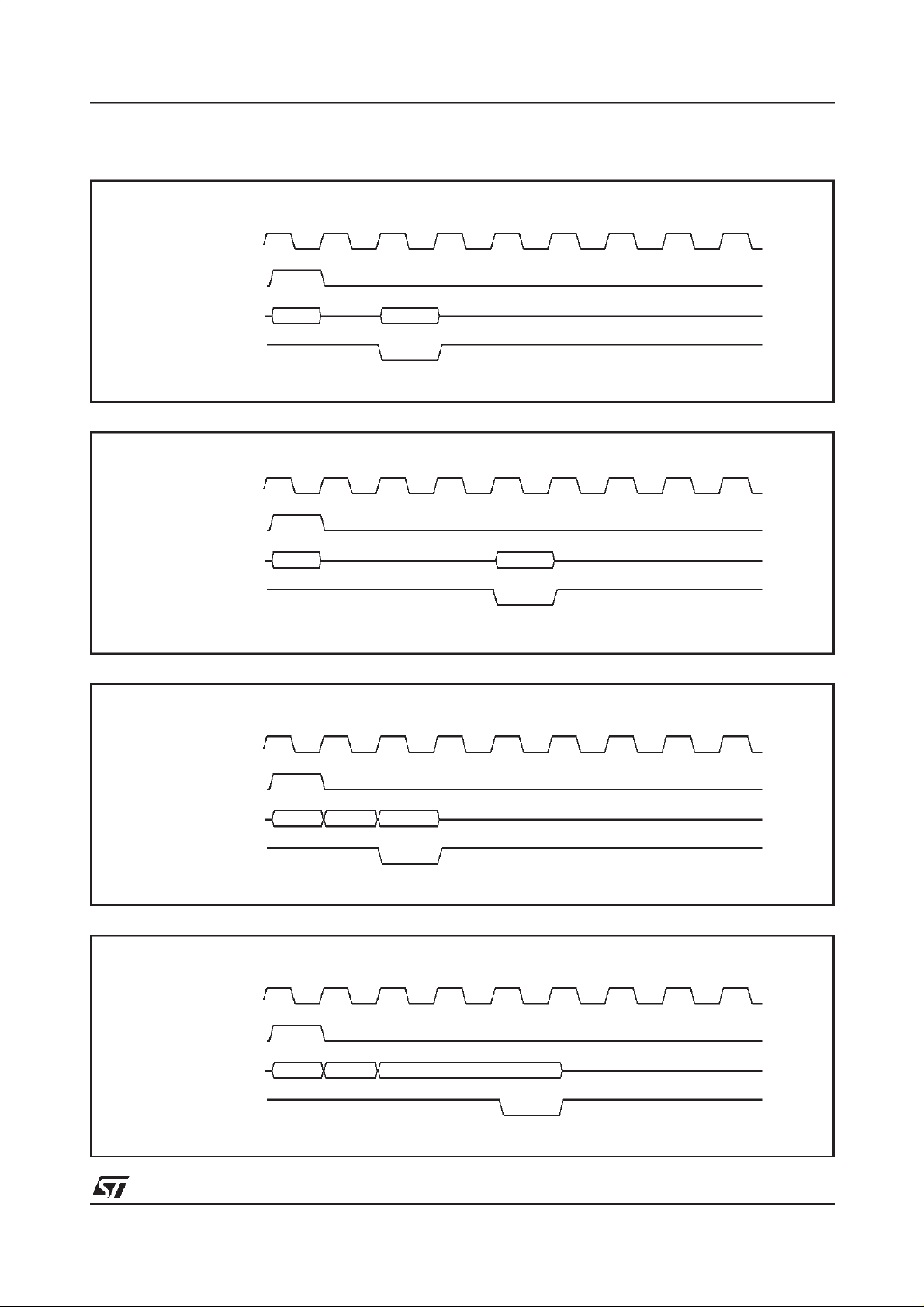
128-BIT 3D MULTIMEDIA ACCELERATOR RIVA128ZX
8.3 TIMING DIAGRAMS
Figure 46. Poll cycle
MPCLK
MPFRAME#
A0 D0
MP_AD[7:0
MPDTACK#
Figure 47. Poll cycle throttled by slave
MPFRAME#
]
MPCLK
A0 D0
MP_AD[7:0
MPDTACK#
]
Figure 48. CPU write cycle
MPCLK
MPFRAME#
MP_AD[7:0
MPDTACK#
]
A0 D
A1
Figure 49. CPU write cycle throttled by slave
MPCLK
MPFRAME#
MP_AD[7:0
MPDTACK#
A0 D
]
A1
47/85
Page 48
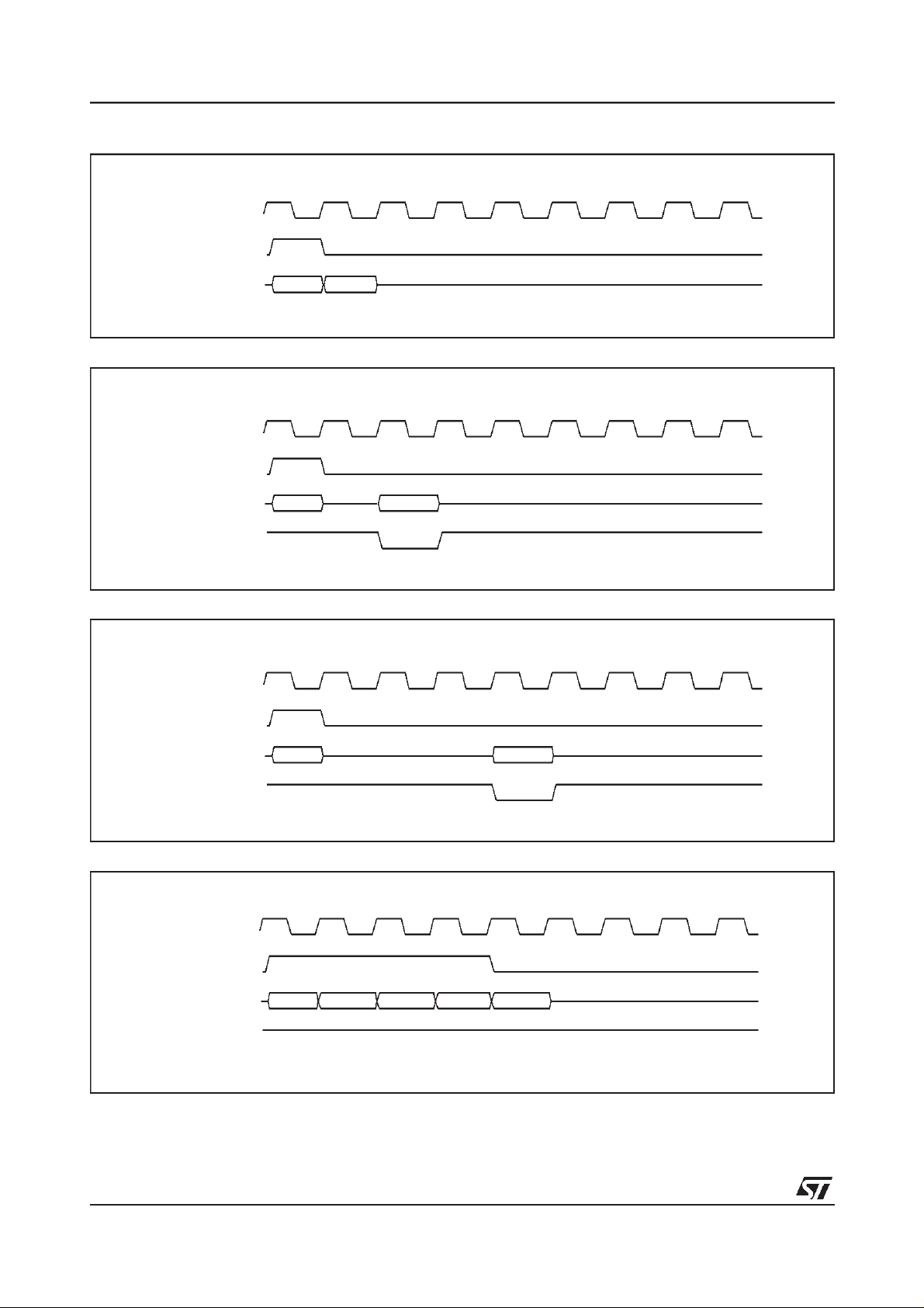
128-BIT 3D MULTIMEDIA ACCELERATORRIVA128ZX
Figure 50. CPU read issue cycle - cannot be throttled by slave
MPCLK
MPFRAME#
A0
MP_AD[7:0
Figure 51. CPU read_receive cycle
MPFRAME#
MP_AD[7:0
MPDTACK#
] A1/D
MPCLK
]
A0 D0
Figure 52. CPU read_receive cycle - throttled by slave
MPCLK
MPFRAME#
A0 D0
MP_AD[7:0
MPDTACK#
]
Figure 53. CD write cycle - terminated by master
MPCLK
MPFRAME#
MP_AD[7:0]
MPDTACK#
A0 D0 D1 D2 D3
48/85
Page 49
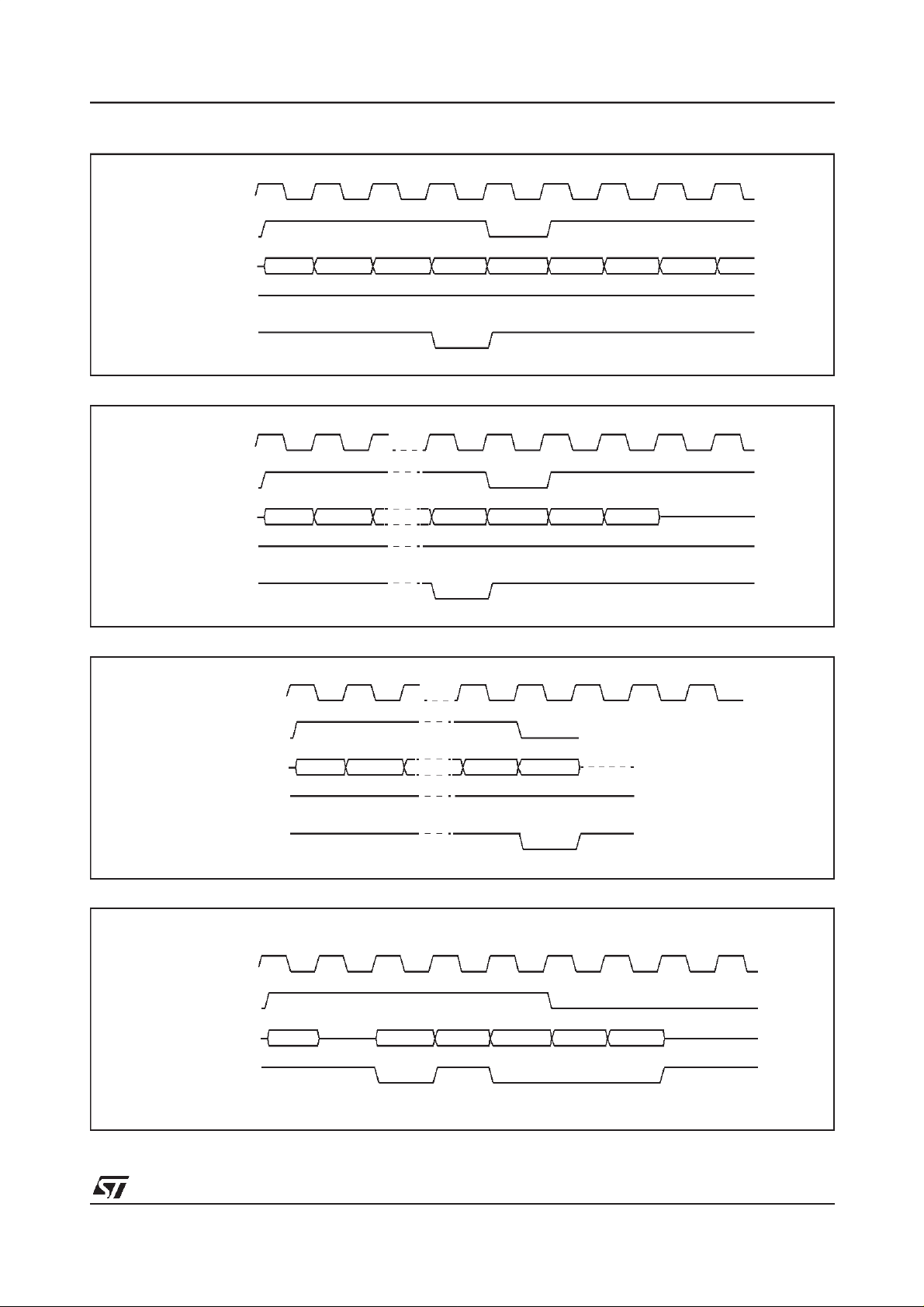
128-BIT 3D MULTIMEDIA ACCELERATOR RIVA128ZX
Figure 54. CD write cycle - terminated by slave in middle of transfer
MPCLK
MPFRAME#
MP_AD[7:0]
MPDTACK#
MPSTOP#
A0 D0 D1 D2 XXX A0 D3 D4
Figure 55. CD write cycle - terminated by slave on byte 31
MPCLK
MPFRAME#
MP_AD[7:0]
MPDTACK#
MPSTOP#
A0 D0 D30 XXX A0 D31
Figure 56. CD write cycle - terminated by slave on byte 32, no effect
MPCLK
MPFRAME#
MP_AD[7:0]
MPDTACK#
MPSTOP#
A0 D0 D30 D31
Figure 57. UCD read cycle, terminated by master, throttled by slave
MPCLK
MPFRAME#
MP_AD[7:0]
MPDTACK#
A0 XXX D1 D2 D3D0
49/85
Page 50
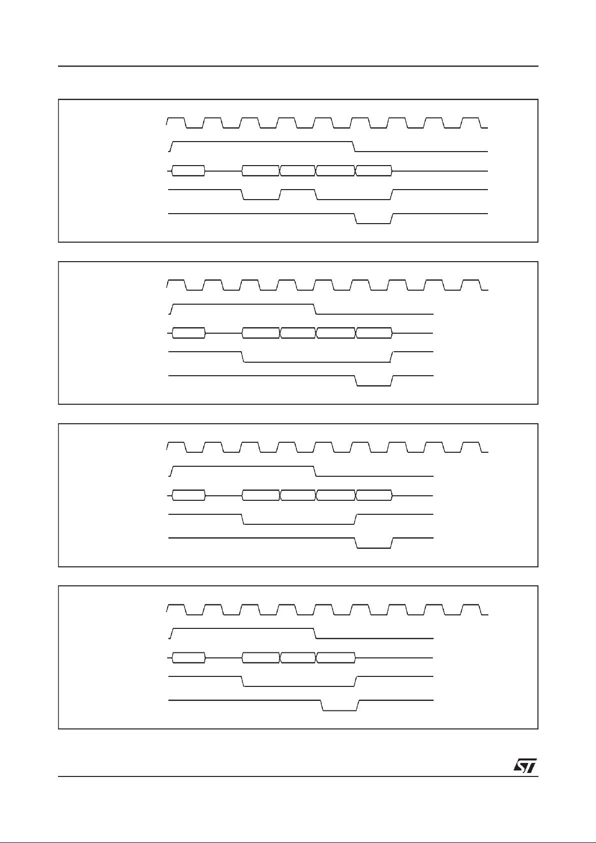
128-BIT 3D MULTIMEDIA ACCELERATORRIVA128ZX
Figure 58. UCD read cycle, terminated by slave, throttled by slave
MPCLK
MPFRAME#
MP_AD[7:0]
MPDTACK#
MPSTOP#
A0 XXX D1 D2D0
Figure 59. UCD read cycle, slave termination after MPFRAME# deasserted, data taken
MPCLK
MPFRAME#
MP_AD[7:0]
MPDTACK#
MPSTOP#
A0 D1 D2 D3D0
Figure 60. UCD read cycle, slave termination after MPFRAME# deasserted, data not taken
MPCLK
MPFRAME#
MP_AD[7:0]
MPDTACK#
MPSTOP#
A0 D1 D2 D3D0
Figure 61. UCD read cycle, slave termination after MPFRAME# deasserted, data taken
MPCLK
MPFRAME#
MP_AD[7:0]
MPDTACK#
MPSTOP#
A0 D1 D2D0
50/85
Page 51
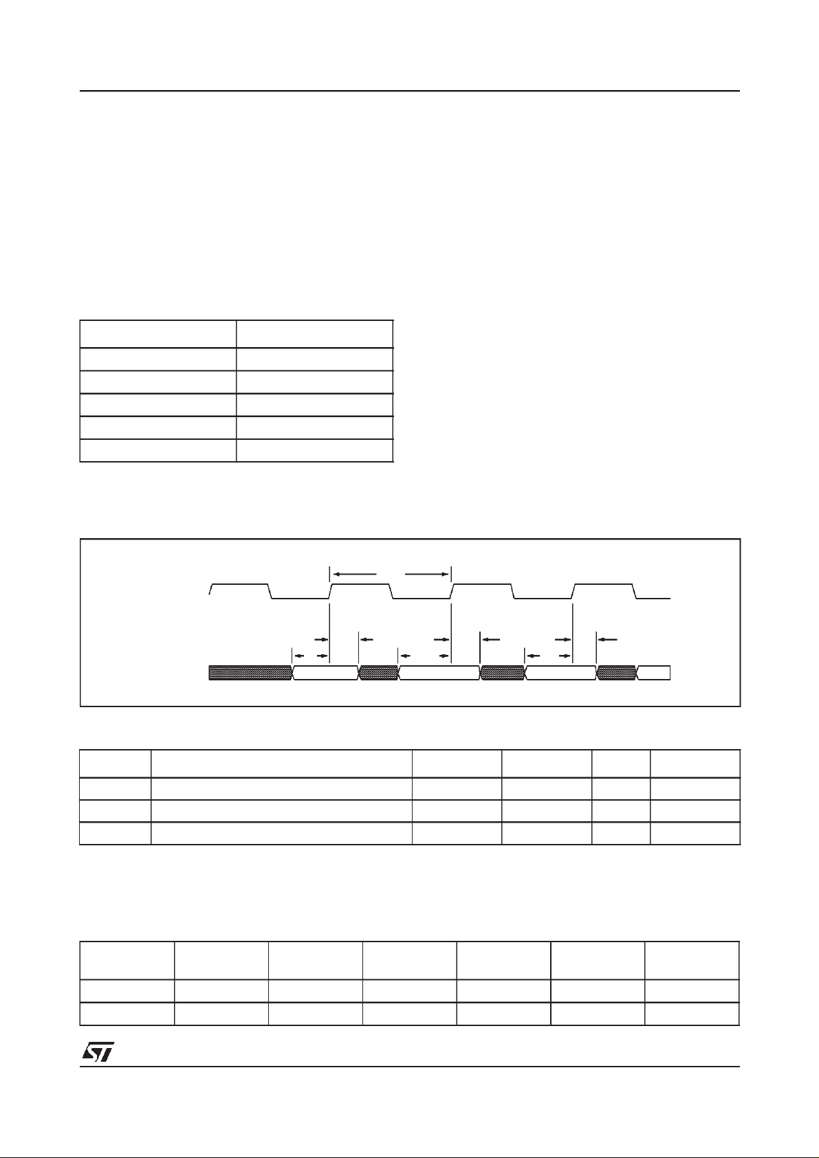
128-BIT 3D MULTIMEDIA ACCELERATOR RIVA128ZX
8.4 656 MASTER MODE
Table 15 shows theVideo Port pin definition when
the RIVA128ZX is configured inITU-R-656 Master
Mode. Before enteringthis mode,RIVA128ZX disables all Video Port devices so that the bus is tristated. The RIVA128ZX will then enable thevideo
656 master device through the serial bus. In this
mode, the video device outputs the video data
continuously at the PIXCLK rate.
Table 15. 656 master mode pin definition
Normal Mode 656 Master Mode
MPCLK PIXCLK
MPAD[7:0] VID[7:0]
MPFRAME# Not used
MPDTACK# Not used
MPSTOP# Not used
656 master mode timing specification
The 656 Master Mode assumes that VID[7:0] and
PIXCLK can be tri-stated when the slave is inac-
tive. If aslave cannot tri-state allits signals, an external tri-state buffer is needed.
Video data capture
Video Port pixel data isclocked into the portby the
external pixel clock and then passed to the
RIVA128ZX’s video capture FIFO.
Pixel data capture is controlled by the ITU-R-656
codes embedded in the data stream; each active
line beginning with SAV (start active video) and
ending with EAV (end active video).
In normal operation, when SAV = x00, capture of
video data begins, and when EAV = xx1, capture
of videodata ends for that line.When VBI(Vertical
Blanking Interval)capture isactive, theserules are
modified.
Figure 62. 656 Master Mode timing diagram
t5
PIXCLK
t3
t4
VID[7:0]
t3
t4
t3
t4
Table 16. ITU-R-656 Master Mode timing parameters
Symbol Parameter Min. Max. Unit Notes
t3 VID[7:0] hold from PIXCLK high 0 ns
t4 VID[7:0] setup to PIXCLK high 5 ns
t5 PIXCLK cycle time 35 ns
NOTE
1 VACTIVE indicates that valid pixeldata is being transmitted across the video port.
Table 17. YUV (YCbCr) byte ordering
1st byte 2nd byte 3rd byte 4th byte 5th (next
dword)
U[7:0] Y0[7:0] V[7:0] Y1[7:0] U[7:0] Y0[7:0] V[7:0]
Cb[7:0] Y0[7:0] Cr[7:0] Y1[7:0] Cb[7:0] Y0[7:0] Cr[7:0]
6th byte 7th byte
51/85
Page 52

128-BIT 3D MULTIMEDIA ACCELERATORRIVA128ZX
8.5 VBI HANDLING IN THE VIDEO PORT
RIVA128ZX supports two basic modes for VBI
data capture.VBI mode1is foruse withthe Philips
SAA7111A digitizer,VBI mode2 isfor usewith the
Samsung KS0127 digitizer.
In VBI mode 1, the region to be captured as VBI
data is set up in the SAA7111Avia the serial interface, and in the RIVA128ZX under software control. The SAA7111A responds by suppressing
generation of SAV and EAVcodes forthe linesselected, and sending raw sample data to the port.
The RIVA128ZX Video Port capture engine starts
capturing VBI data at an EAV code in the line last
active and continues to capture data without a
break until it detects the next SAV code. VBI capture is then complete for that field.
In VBI mode 2, the region to be captured as VBI
data is set up in asimilar manner.The KS0127 responds by enabling VBIdata collection only during
the lines specified and framed by normal ITU-R656 SAV/EAV codes. The RIVA128ZX Video Port
capture engine starts capturing data at an SAV
code controlled by the device driver, and continues capturing data under control of SAV/EAV
codes until a specific EAV code identified by the
device driver issampled. VBI captureis then complete for that field. The number of bytes collected
will vary depending on the setup of the KS0127.
8.6 SCALING IN THE VIDEO PORT
The RIVA128ZX Video Port allows any arbitrary
scale factorbetween 1and 31. For best resultsthe
scale factors of 1, 2, 3, 4, 6, 8, 12, 16, and 24 are
selected to avoid filtering losses. The Video Port
decimates in the y-direction, dropping lines every
few lines depending on the vertical scaling factor.
The intention is to support filtered downscaling in
the attached video decoder.
52/85
Page 53
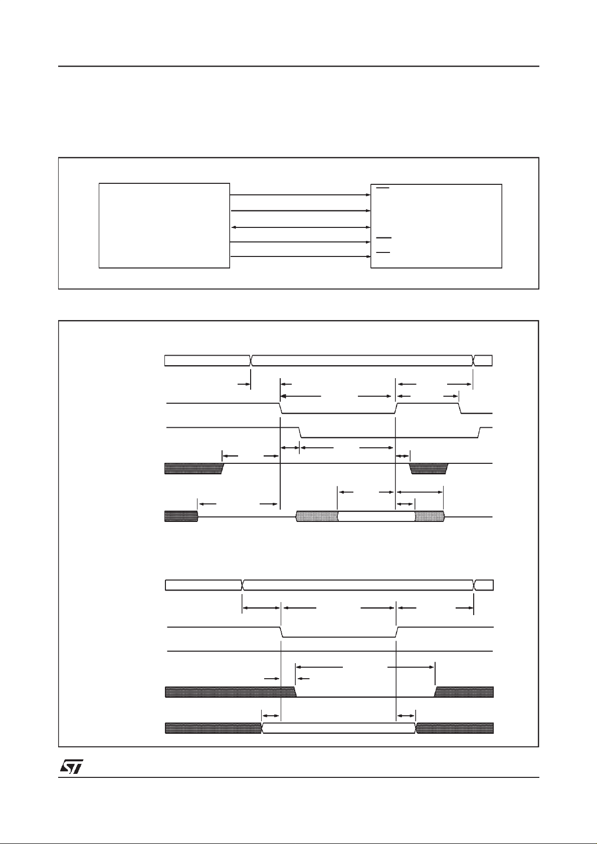
128-BIT 3D MULTIMEDIA ACCELERATOR RIVA128ZX
9 BOOT ROM INTERFACE
BIOS andinitialization code forthe RIVA128ZXis accessed from a 32KByteROM. TheRIVA128ZX memory bus interface signalsFBD[15:0] and FBD[31:24] are used toaddress and access one of 64KBytesof
data respectively. The unique decode to theROM device is provided by the ROMCS# chip select signal.
Figure 63. ROM interface
ROMCS#
FBD[15:0]
RIVA128ZX
FBD[31:24]
FBD[17]
FBD[16]
ROM interface timing specification
Figure 64. ROM interface timing diagram
ROM Read
FDB[15:0]
ROMCS#
OE# (FBD[16])
tBRV
WE# (FBD[17])
BAS
t
tBOS
address
tBRCS
tBOH
CS
A[15:0]
D[7:0]
WE
OE
ROM
tBAH
tBRCA
tBRH
FDB[31:24]
FDB[15:0]
ROMCS#
OE# (FBD[16])
WE# (FBD[17])
FDB[31:24]
ROM Write
tBAS
tBDBZ
tBDS
tBDH
data
address
tBRCS tBAH
tBWL
t
BWS
tBWDS tBWDH
data
tBDZ
53/85
Page 54

128-BIT 3D MULTIMEDIA ACCELERATORRIVA128ZX
Table 18. ROM interface timing parameters
Symbol Parameter Min. Max. Unit Notes
t
BRCS ROMCS# active pulse width 20TMCLK-5 ns
BRCA ROMCS# precharge time TMCLK-5 ns
t
BRV Read valid to ROMCS# active TMCLK-5 ns
t
BRH Read hold from ROMCS# inactive TMCLK-5 ns
t
BAS Address setup to ROMCS# active TMCLK-5 ns
t
BAH Address hold from ROMCS# inactive TMCLK-5 ns
t
BOS OE# low from ROMCS# active ns 2
t
BOH OE# low to ROMCS# inactive ns 3
t
BWS WE# low from ROMCS# active ns 2
t
BWL WE# low time ns 3
t
BDBZ Data bus high-z to ROMCS# active TMCLK-5 ns
t
BDS Data setup toROMCS# inactive 10 ns
t
BDH Data hold from ROMCS# inactive 0 ns
t
BDZ Data high-z from ROMCS# inactive TMCLK-5 ns
t
BWDH Write data hold from ROMCS# inactive 0.5TMCLK-5 ns
t
BWDS ROM write data setup to ROMCS# active TMCLK-5 ns
t
NOTE
MCLK is the period of the internal memory clock.
1T
2 This parameter is programmable in the range 0 - 3 MCLK cycles
3 This parameter is programmable in the range 0 - 15 MCLK cycles
54/85
Page 55

128-BIT 3D MULTIMEDIA ACCELERATOR RIVA128ZX
10 POWER-ON RESET CONFIGURATION
The RIVA128ZX latches its configuration on the
trailing edge of RST# and holds its system bus interface ina high impedancestate untilthis time.To
accomplish this, pull-up or pull-down resistors are
connected to the FBA[9:0] pins as appropriate.
Since there are no internal pull-up orpull-down resistors and the address busshould be floating during reset, a resistor value of up to 47KΩ, but no
less than 10KΩ, should be sufficient.
The power-on resetconfiguration seen bythe chip
may be overwritten. Theexternal FBA[9:0]configuration is stored in latches. An additional writable
register, containing all of the configuration bits
Power-on reset FBA[9:0] bit assignments
9876543210
AGP
Mode
[9] AGP Mode. This bit selects whether the AGP bus 1X or 2X mode is enabled.
0 = AGP 2X mode enabled
1 = AGP 1X mode enabled
[8:7] TV Mode. These bits select the timing format when TV mode is enabled.
00 = Reserved
01 = NTSC
10 = PAL
11 = TV mode disabled
[6] Crystal Frequency.This bit should match the frequency of the crystal orreference clock connect-
ed to XTALOUT and XTALIN.
0 = 13.500MHz (used where TV output may be enabled)
1 = 14.31818MHz
[5] Host Interface
0 = PCI
1 = AGP
[4] RAM Width
0 = 64-bit framebuffer data bus width (the upper 64-bit data bus and byte selects are tri-state)
1 = 128-bit framebuffer data bus width
Although a10KΩ resistor is used to strap the default state of this bit in RIVA 128 and RIVA128ZX
reference designs, it is ignored by the video BIOS which auto-detects the memorytype and configures the RIVA128ZX appropriately.
[3] APCI Supported
0 = ACPI registers not supported. This provides compatibility with the PCI register configuration
as implemented by RIVA 128. The RIVA128ZX will be identified by DEVICE_ID_CHIP = 0x18 at
PCI Configuration offset 0x0.
1 = ACPI registers supported. Power management registers supported in PCI configuration
space. The RIVA128ZX willbe identified by DEVICE_ID_CHIP = 0x19 at PCI Configuration offset
0x0.
TV Mode Crystal Host
Interface
plus an additional STRAP_OVERWRITE bit (register bit [11]), exists in parallel with the latches to
allow thehost tooverwrite the external value.Writing to address BOOT_0 (0x00101000) writes into
this register.
The STRAP_OVERWRITE bit controls whether
the latches or the parallel writable register are selected. When STRAP_OVERWRITE is set to 0,
the latched FBA[9:0] configuration is selected.
When set to 1, the chip uses the register value.
Reading from address BOOT_0 reads either the
configuration latches or the parallel register depending on the STRAP_OVERWRITE setting.
RAM
Width
ACPI
Sup-
ported
RAM
Type
Sub-
Vendor
Bus
Speed
55/85
Page 56
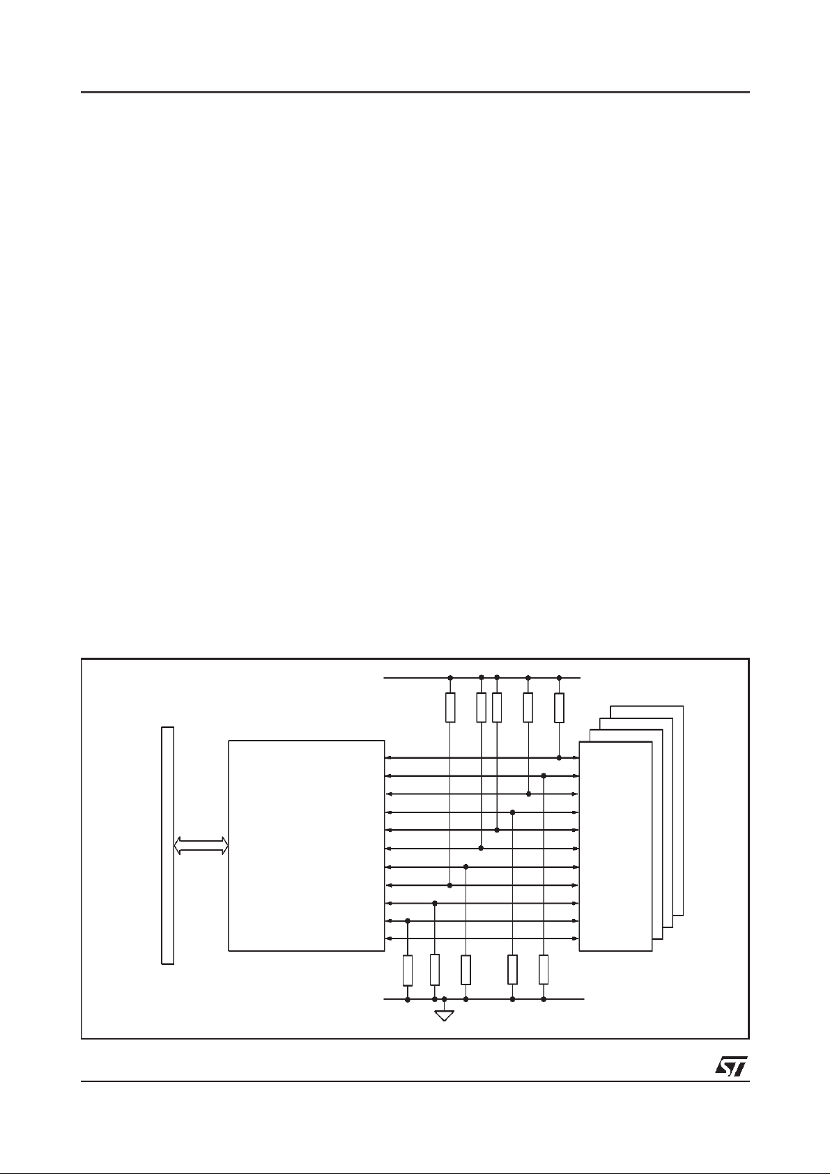
128-BIT 3D MULTIMEDIA ACCELERATORRIVA128ZX
[2] RAM Type
0 = 16Mbit, 2 or 4 internal bank SGRAM or 16Mbit SDRAM. The BIOS should testthe memory to
determine whether it supports 2 or 4 internal banks.
1 = 8Mbit, 2 internal bank SGRAM.
Although a10KΩ resistor is used to strap the default state of this bit in RIVA 128 and RIVA128ZX
reference designs, it is ignored by the video BIOS which auto-detects the memorytype and configures the RIVA128ZX appropriately.
[1] Sub-Vendor. This bit indicates whether the PCI Subsystem Vendor field is located in the system
motherboard BIOS oradapter cardVGABIOS. Ifthe SubsystemVendorfield islocated inthe system BIOS it must be written by the system BIOS to the PCI configuration space prior to running
any PnP code.
0 = System BIOS (Subsystem Vendor ID and Subsystem ID set to 0x0000)
1 = Adapter card VGA BIOS (Subsystem Vendor ID and Subsystem ID read from ROM BIOS at
location 0x54 - 0x57)
[0] Bus Speed. This bit indicates the value returned in the 66MHz bit in the PCI Configuration regis-
ters.
0 = RIVA128ZX PCI interface is 33MHz
1 = RIVA128ZX is 66MHz capable
The following example configuration is shown in Figure65:
• Subsystem Vendor ID initialized to 0 and writeable by system BIOS (see Appendix A, page 76)
• 8Mbit, 2 internal bank, SGRAM
• 128-bit framebuffer interface
• AGP 2X mode enabled including 66MHz PCI 2.1 compliant subset
• Using 13.5000MHz crystal
• TV output mode is NTSC
Figure 65. Example motherboard configuration
VDD (3.3V)
FBA[0
]
FBA[1]
FBA[2]
FBA[3]
AGP
RIVA128ZX
FBA[4]
FBA[5]
FBA[6]
FBA[7]
FBA[8]
FBA[9]
FBA[10]
SGRAM
array
56/85
10KΩ
Page 57
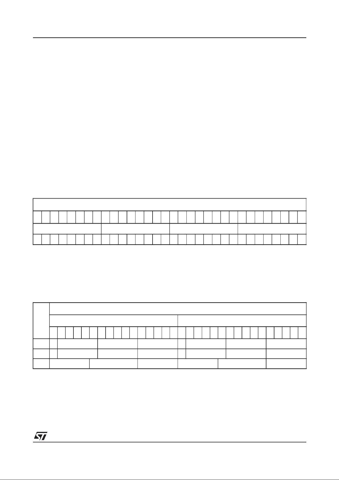
128-BIT 3D MULTIMEDIA ACCELERATOR RIVA128ZX
11 DISPLAY INTERFACE
11.1 PALETTE-DAC
The Palette-DAC integrated into the RIVA128ZX
supports a traditionalpixel pipeline withthe following enhancements:
• Support for 10:10:10, 8:8:8, 5:6:5 and 5:5:5 di-
rect color pixel modes
• Support for dynamic gamma correction on a
pixel by pixel basis
• Support for mixed indexed color and direct col-
or pixels
• 256 x 24 LUT for 8-bit indexed modes
• High quality video overlay
- Accepts interlaced video fields allowing a reduction inmemory buffering requirements while
incorporating temporal averaging
- Line buffer for horizontal and vertical interpolation of video streams up to square pixel PAL
resolution
- 3x2 multitap interpolating filter with image
sharpening
- Color key in all color pixel modes
- High quality YUV to RGB conversion with
chrominance control.
11.2 PIXEL MODES SUPPORTED
8-bit indexed color
In the 8-bit indexed color each 32-bit word contains four 8-bit indexed color pixels, each comprising bits
b[7:0] as shown below.
Pixel formats (FBD[31:0])
31 30 29 28 27 26 25 24 23 22 21 20 19 18 17 16 15 14 13 12 11 10 9 8 7 6 5 4 3 2 1 0
Pixel 3 Pixel 2 Pixel 1 Pixel 0
b7 b6 b5 b4 b3 b2 b1 b0 b7 b6 b5 b4 b3 b2 b1 b0 b7 b6 b5 b4 b3 b2 b1 b0 b7 b6 b5 b4 b3 b2 b1 b0
NOTE
1 This 32-bit representation can be extended to 64-bit and 128-bit widths by duplicating the 32-bit word in little-endian format.
16-bit direct color modes (5:6:5 direct and 5:5:5 with and without gamma correction)
In 5:5:5 colormodes bit 15 of each pixel can be enabled to select whether pixel data bypasses the LUT to
feed the DACs directly, or indirectly, through the LUT, to allow gamma correction to be applied. If not enabled then the bypass mode will always be selected, and the LUT powered down. The 16-bit modes include a 5:6:5format which always bypasses the LUT.
Pixel formats (FBD[31:0])
5:6:5
mode
313029282726252423222120191817161514131211109876543210
0 0 Red gamma Green gamma Blue gamma 0 Red gamma Green gamma Blue gamma
0 1 Red bypass Green bypass Blue bypass 1 Red bypass Green bypass Blue bypass
1 Red bypass Green bypass Blue bypass Red bypass Green bypass Blue bypass
NOTE
1 This 32-bit representationcan be extended to 64-bit and128-bit widths by duplicating the 32-bit word in little-endian for-
mat.
Pixel 1 Pixel0
32-bit direct color (8:8:8 with gamma correction or 10:10:10 direct)
In 32-bit color mode bit 31 of each pixel selects whether pixel data bypasses the LUT, to feed the DACs
directly orindirectly, through theLUT, toallow gamma correctionto beapplied. Inthe tablebelow theRed,
Green and Blue bypass bits are shown individually as R[9:0], G[9:0], and B[9:0] because, in the bypass
57/85
Page 58
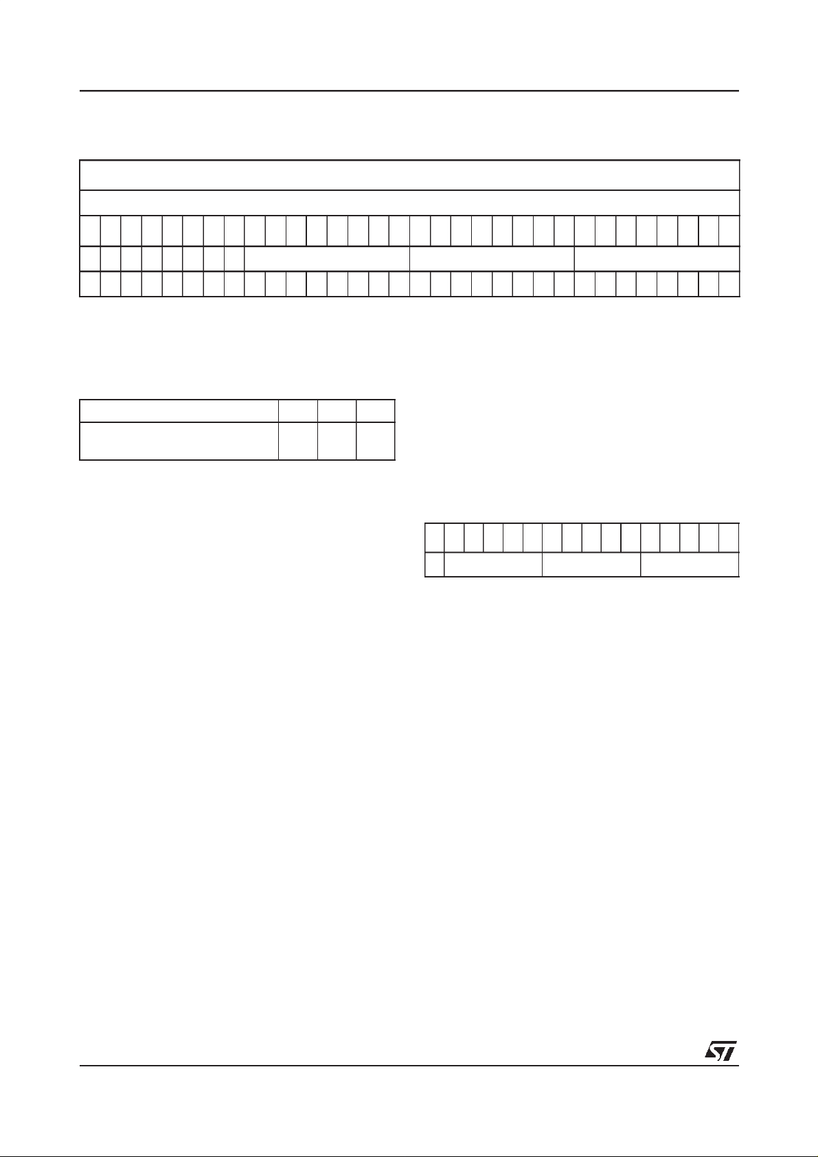
128-BIT 3D MULTIMEDIA ACCELERATORRIVA128ZX
mode pixel format, the least significantbits of each color arelocated separately in the top byte of the pixel.
This also permits an 8:8:8 mode without gamma with <1% error if desired.
Use of pixel input pins (FBD[31:0])
Pixel 0
31 30 29 28 27 26 25 24 23 22 21 20 19 18 17 16 15 14 13 12 11 10 9 8 7 6 5 4 3 2 1 0
0XXXXXXX Redgamma Green gamma Blue gamma
R1 R0 G1 G0 B1 B0 R9 R8 R7 R6 R5 R4 R3 R2 G9 G8 G7 G6 G5 G4 G3 G2 B9 B8 B7 B6 B5 B4 B3 B2
1X
NOTE
This 32-bit representation canbe extendedto 64-bit and 128-bit widths by duplicating the 32-bit word in little-endian format.
Limitations on line lengths
Table 19. Permitted line length multiples
bpp 8 16 32
Number of pixels that the line
length must be a multiple of
421
11.3 HARDWARE CURSOR
The RIVA128ZXsupports a 32x32 15bpp full color
hardware cursor as defined by Microsoft Windows.
• Full color 5:5:5 format
• Pixel complement
• Transparency
• Pixel inversion
The cursor patternis stored ina 2KByte bitmap located inoff-screen framestore.Details of programming the hardware cursor are given in the
RIVA128ZX
Programming Reference Manual
[2].
Registers control cursor enabling/disabling, location of cursor bitmap and cursor display coordinates. Thecursor data and it’s positionshould only
be changed during frame flyback. The cursor
should bedisabled when not being used.
Cursor format
15 14 13 12 11 10 9 8 7 6 5 4 3 2 1 0
A Red Green Blue
The 5-bit RGB color components are expanded to
10 bits per color before combining with the graphics displaydata. Theexpanded10-bit coloris composed of the5-bit cursor colorreplicated in the upper and lower 5-bit fields. The cursor pixels are
combined such that the cursor will overlay a video
window if present.
Cursor pixel bit 15 (A) is the replace mode bit.
When A=1, the cursor pixel replaces the normal
display pixel. If A=0, the expanded 30 bits of the
cursor color are XORed with the display pixel to
provide the complement of the background color.
Cursor pixels can be made transparent (normal
display pixel is unmodified)by setting to a value of
0x0000. To invert the bits of the normal display
pixel, the cursor pixel should be set to 0x7FFF.
58/85
Page 59

128-BIT 3D MULTIMEDIA ACCELERATOR RIVA128ZX
11.4 SERIAL INTERFACE
The RIVA128ZX serial interface supports connec-
tion to DDC1/2B, DDC2AB and DDC2B+ compliant monitors and to serial interface controlled video decodersand tuners. Supportedvideo decoder
chips include Philips SAA7110, SAA7111A, ITT
3225 and Samsung KS0127. For details of address locations and protocols applying to specific
parts refer to the appropriate manufacturer’s
datasheet.
The serial interfacein RIVA128ZX requires operation under software control to provide emulation of
the interface standard. RIVA128ZX can act as a
master for communication with slave devices like
those mentioned above. It also acts as a master
when interfacing to a DDC1/2compatible monitor.
Although it is not Access.bus compatible, it can
communicate with a DDC2AB compatible monitor
via the DDC2B+ protocol. (No other Access.bus
peripherals can be attached although other serial
devices may co-reside on the DDC bus). The
RIVA128ZX can clockstretch incoming messages
in the eventthat thesoftware handlerisinterrupted
by another task.
59/85
Page 60
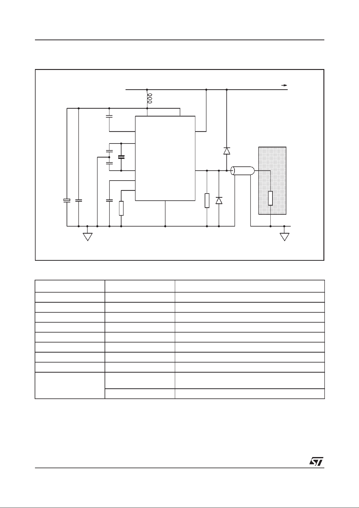
128-BIT 3D MULTIMEDIA ACCELERATORRIVA128ZX
11.5 ANALOG INTERFACE
Figure 66. Recommended circuit (crystal circuit is for designs not supporting TV out)
VDD
Local PLLVDD plane
∗
C5
C3
X1
C4
∗
C2
C1
∗ Thesecomponents should be placed as close to the RIVA128ZX outputs as possible
C6
R1
∗
L1
PLLVDD
COMP
XTALIN
RIVA128ZX
XTALOUT
VREF
RSET
GND
DACVDD
VDD
RED,
GREEN,
BLUE
R2-R4
D1-D3
∗
Power supply
D4-D6
Monitor
75Ω
cable
75Ω
Table 20. Table of parts for recommended circuit (Figure 66)
Part number Value Description
C1 22µF tantalum capacitor
C2 100nF surface mount capacitor
C3, C4 10pF surfacemount capacitor
C5, C6 10nF surfacemount capacitor
R1 147Ω 1% resistor
R2-R4 75Ω 1% resistor
D1-D6 1N4148 protection diodes
L1 1µH inductor
X1 13.50000MHz series resonant crystal (used where TV output may be
required)
14.31818MHz series resonant crystal
60/85
Page 61
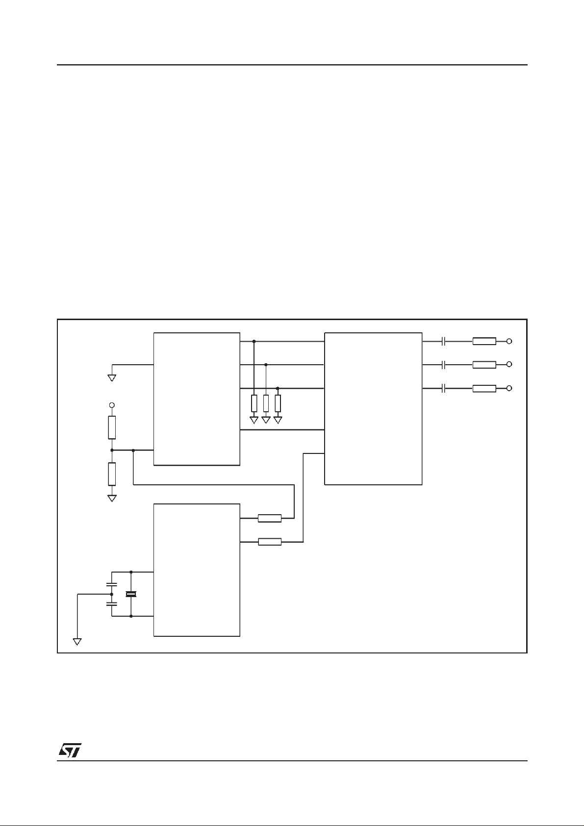
128-BIT 3D MULTIMEDIA ACCELERATOR RIVA128ZX
11.6 TV OUTPUT SUPPORT
Reference clock options
The RIVA128ZX supports two synthesizer reference clock frequencies; 13.5MHz and
14.31818MHz. The reference clock frequency is
determined by a crystal or reference clock connected to theXTALIN andXTALOUT pins. Where
TV-out is supported, XTALOUT should be driven
by a 13.5MHz reference clock derived from an external NTSC/PAL clock source as illustrated in
Figure 67. The clock frequency should match the
power-on configuration setting described in Section 10, page 55.
PAL/NTSC TV interface
The RIVA128ZX supports TV output through an
external Analog Devices AD722 PAL/NTSC RGB
encoder chip as shown in Figure 67. A MicroClock
Figure 67. TV output implementation
MK2715 NTSC/PAL clock chip provides a common source for synchronization of the pixel and
subcarrier clocks. In TV output modes the
RIVA128ZX XTALOUT pin must be externally
driven from the MK2715 reference clock output,
with XTALIN tied to GND.
The MK2715 requires a number of external components for proper operation. For crystal input a
parallel resonant 13.5000MHz crystal is recommended, with a frequency tolerance of 50ppm or
better. Capacitors should be connected from X1
and X2to GNDas shownin Figure67. Alternatively a clock input (e.g. ClockCan) can be connected
to X1,leaving X2disconnected. Furtherdetails are
given in the MK2715 datasheet [8].
5V
220Ω
330Ω
27pF
27pF
13.50000MHz
crystal
XTALIN
RIVA128ZX
VIDHSYNC
XTALOUT
REFOUT
X1/ICLK
MK2715
NTSC/PAL
Clock Source
X2
R
G
B
4XCLK
33Ω
33Ω
75Ω
RIN
GIN
BIN
AD722 TV
RGB Encoder
HSYNC
FIN
YOUT
COUT
CVOUT
220µF
220µF
220µF
75Ω
75Ω
75Ω
61/85
Page 62
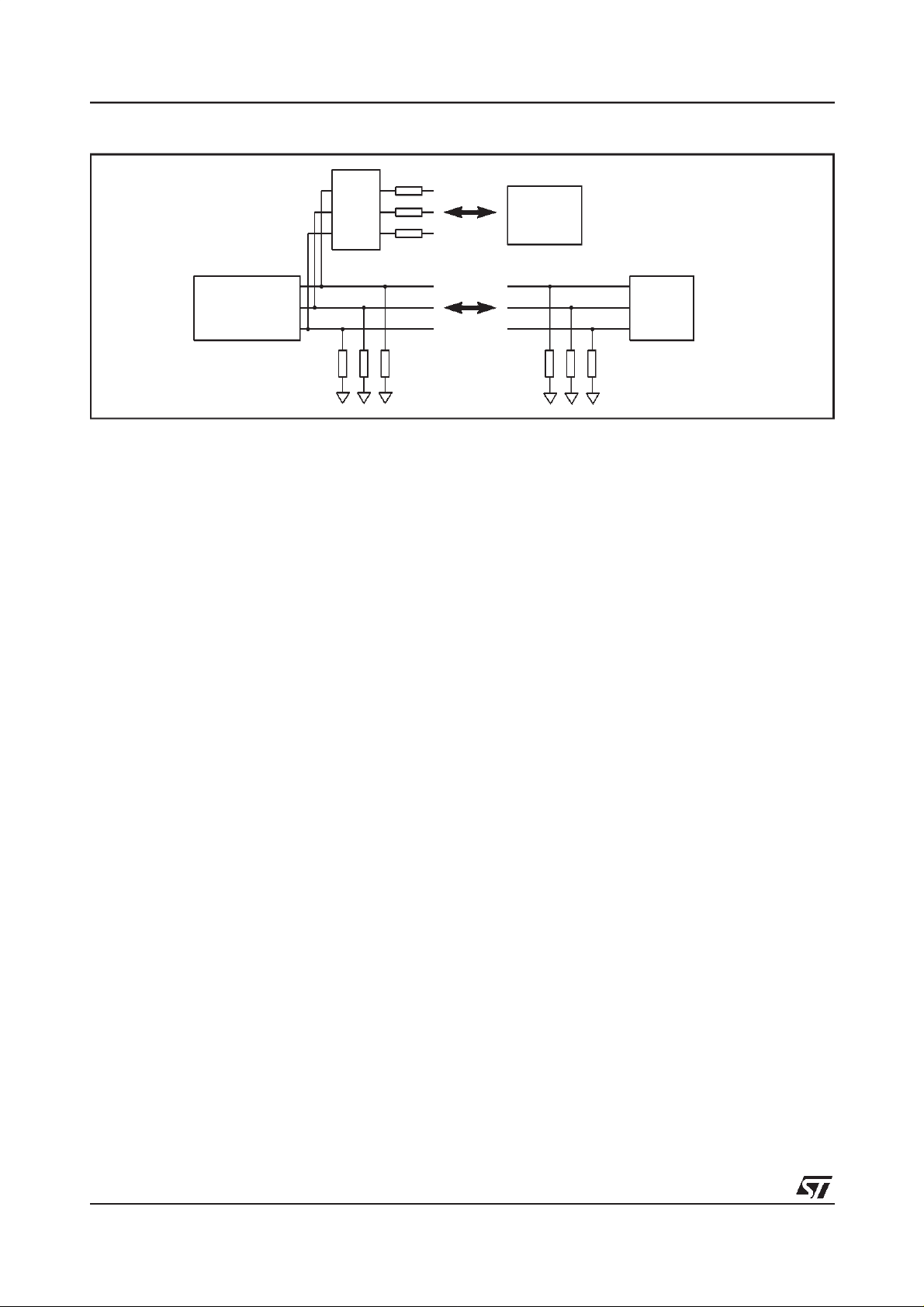
Figure 68. Interface to monitor or television
128-BIT 3D MULTIMEDIA ACCELERATORRIVA128ZX
C
Y/C
75
Y
75
75
TV RGB
Encoder
RIVA128ZX
R
G
B
R
G
B
75 75 75
Monitor detection
Figure 68 shows thetypical connectionof a television or computer monitor to the RIVA128ZXs’
DAC outputs. The RIVA128ZX expects only one
output display device to be connected at a time
and does not support simultaneous output to both
the monitor and television.
During system initialization, the BIOS detects if a
monitor is connected by sensing thedoubly-terminated 75Ω load (net 37.5Ω). When no monitor is
connected, only thelocal 75Ω loadis detectedand
the RIVA128ZX switches to television output
mode. The BIOS sets the CRTC registers to generate the appropriate timing forthe local television
standard and the DACs are adjusted to compensate for the single 75Ω load.
Monitor mode is always selected if amonitor isdetected since it is assumed to be the output device
of choice, having a higher display fidelity thantelevision.
Timing generation
Televisions contain two Phase-Locked Loops
(PLLs). One PLL locks the horizontal frequency
and is used to synchronize horizontal and vertical
flyback, and to keep the activevideo region stable
and centered. The second PLL locks the color
subcarrier frequency (NTSC 3.5794545MHz or
PAL 4.43361875MHz). The color subcarrier is
used as a phase reference to extract the color information from the television signal.
The RIVA128ZX encodes horizontal and vertical
timing on a composite sync signal. Using a
13.5000MHz reference clock, the RIVA128ZXtiming generator creates ITU-R-601 NTSC and PAL
compliant horizontal timing with only ppm (parts
per million) error. The RIVA128ZX does not use
PAL/NTSC
Television
Monitor
75 75 75
the color subcarrier clock internally. The reference
clock source can be located on the television upgrade module with the video encoder and TV output connectors, thus lowering the base system
cost.
Flicker filter
RIVA128ZX provides an optional flicker filtering
feature for TV and interlaced displays.
Without flicker filtering, elements of an image
present on either the odd orthe evenfield, but not
both, are seen to flicker or shimmer obtrusively.
This is a problem especially with 1-pixel-wide horizontal lines often originating from computer generated GUI displays.
Flicker filtering causes a slight smearing of pixels
in thevertical direction. Thistrades off image quality versus flicker. The displayed pixel contains a
proportion ofthe datafor the pixel onthat line,plus
a smaller proportion of the data of the equivalent
pixel on the line above and on the line below.
Overall, the proportions add up to 1 so that the
brightness ofthe screendoes notalter and the pixel data does not get clipped.
Flicker filtering only takes place onpixel data from
the framestore - the pattern written into the cursor
already has flicker removed. No flicker removal is
performed on video images.
Overscan and underscan
The RIVA128ZX supports overscan and underscan in the horizontal and vertical directions using
hardware scaling. Underscanallows 640x480 resolution tofit onto NTSCdisplays and 800x600 resolution to fit onto PAL displays. Scaling canbe adjusted and controlled by software to suit specific
TV requirements. The TV output image position is
also software controllable.
62/85
Page 63
128-BIT 3D MULTIMEDIA ACCELERATOR RIVA128ZX
12 IN-CIRCUIT BOARD TESTING
The RIVA128ZX has a number of features designed to support in-circuit board testing. These include:
• Dedicated test mode input and dual-function test mode select pins selecting the following modes:
- Pin float
- Parametric NAND tree
- All outputs driven high
- All outputs driven low
• Checksum test
• Test registers
12.1 TEST MODES
Primary test control is provided by the dedicated TESTMODE input pin. The RIVA128ZX is in normal op-
erating mode whenthis pin isdeasserted. WhenTESTMODE is asserted,MP_AD[3:0] are reassignedas
TESTCTL[3:0] respectively. Test modes are selected asynchronously through a combination of the pin
states shown in Table 21.
Table 21. Test mode selection and descriptions
Test mode TESTCTL[3:0] Description
3210
Parametric
NAND tree
Pin float 1 1 0 0 All pin output drivers are tristated in thistest mode so that pin leakage
Outputs high 1 1 1 0 All pin output drivers drive a high output state in this test mode so that
Outputs low 1 1 1 1 All pin output drivers drive a low output state in this test mode so that out-
1 0 1 0 A single parametric NAND tree is provided to give a quiescent environ-
ment in which to test VIL and VIH without requiring core activity.
This capability is provided in the pads by chaining all I and I/O paths to-
gether via two input NAND gates. The chain begins with one input of the
firstNAND gate tied to VDD while the other input is connected to the first
devicepin onthe NANDtree. The output of this gate then becomes theinput of the next NAND gate in the tree and so on untilall pad input paths
havebeen connected. The finalNANDgate output is connected toan output-only pin whose normal functionality is disabled in NAND treemode.
The NAND tree length is thereforeequal tothe numberof I and I/O pins in
the RIVA128ZX. Output -only pins are not connected into the NAND tree.
current (IIL,IIH,IOZL,IOZH) can be measured.
output high voltage (VOHat IOH) can be measured.
put low voltage (VOL at IOL) can be measured.
12.2 CHECKSUM TEST
The RIVA128ZX hardware checksum feature supports testingof theentire pixel datapath at full video
ratesfromthe framebufferthrough totheDACinputs.
Each of the three RGB colors can be tested to provide a correlation between the intended and actual
display.Checksums are accumulated during active
(unblanked) display.Note that the checksum mechanism does not check the DAC outputs (i.e. what is
physically being displayedon themonitor).
Fora given image (which can be a realapplication’s
image or aspecially prepared testcard), theoretically derived checksum values can be calculated for a
selected RGB color, which are then compared with
the RIVA128ZXhardware checksum value.Alternatively the checksum value from a known good chip
can be used as the reference.
Hardwarechecksum accumulation isnotaffectedby
the horizontal and vertical synchronization waveforms or timings. Any discrepancy between the calculated and RIVA128ZX hardware accumulated
checksum values therefore indicates a problem in
the device or system being tested. Details of programming the RIVA128ZX checksum are given in
the RIVA128ZX
Programming Reference Manual
[2].
63/85
Page 64
128-BIT 3D MULTIMEDIA ACCELERATORRIVA128ZX
13 ELECTRICAL SPECIFICATIONS
13.1 ABSOLUTE MAXIMUM RATINGS
Symbol Parameter Min. Max. Units Notes
VDD/AVDD DC supply voltage 3.6 V
Voltage on input and outputpins GND-1.0 VDD+0.5 V 2
TS Storage temperature (ambient) -55 125 °C
TA Temperature under bias 0 85 °C
Analog output current (per output) 45 mA
DC digitaloutput current (per output) 25 mA
NOTES
1 Stresses greater than those listed under ‘Absolute maximum ratings’ may cause permanent damage to the device. This
is astress rating only and functional operationof the deviceat these or any other conditions above those indicatedin the
operational sections ofthisspecification is notimplied. Exposure to absolute maximum rating conditionsfor extended periods may affect reliability.
2 For 3V tolerant pins VDD = 3.3V± 0.3V, for 5V tolerant pins (PCI, Video Port and Serial interfaces) VDD = 5V± 0.5V
13.2 OPERATING CONDITIONS
1
Symbol Parameter Min. Typ. Max. Units Notes
TC Case temperature 120 °C
13.3 DC SPECIFICATIONS
Table 22. DC characteristics
Symbol Parameter Min. Typ. Max. Units Notes
VDD Positive supply voltage 3.135 3.3 3.465 V
IIN Input current (signal pins) ±10 µA1,2
Power dissipation 3.7 W
NOTES
1 Includes high impedanceoutput leakage for all bi-directionalbuffers with tri-state outputs
2 VDD = max, GND ≤ VIN ≤ VDD
Table 23. Parameters applying to PCI and AGP interface pins
Symbol Parameter Min. Typ. Max. Units Notes
CIN Input capacitance 5 10 pF 1
COUT Output load capacitance 5 50 pF 1
Parameters for 5V signaling environment only:
VIH Input logic 1 voltage 2.0 5.75 V
VIL Input logic 0 voltage -0.5 0.8 V
VOH Output logic 1 level 2.4 V
VOL Output logic 0 level 0.55 V
IOH Output load current, logic 1 level -2 mA
IOL Output load current, logic0 level 3 or 6 mA 2
Parameters for 3.3V and AGPsignaling environments only:
VIH Input logic 1 voltage 0.475VDD VDD+0.5 V
64/85
Page 65
128-BIT 3D MULTIMEDIA ACCELERATOR RIVA128ZX
Symbol Parameter Min. Typ. Max. Units Notes
VIL Input logic 0 voltage -0.5 0.325VDD V
VOH Output logic 1 level 0.9VDD V
VOL Output logic 0 level 0.1VDD V
IOH Output load current, logic 1 level -0.5 mA
IOL Output load current, logic0 level 1.5 mA
NOTE
1 Tested but notguaranteed.
2 3mA for all signals except PCIFRAME#, PCITRDY#, PCIIRDY#, PCIDEVSEL# and PCISTOP# which have IOL of 6mA.
13.4 ELECTRICAL SPECIFICATIONS
Table 24. Parameters applying to all signal pins except PCI/AGP interfaces
Symbol Parameter Min. Typ. Max. Units Notes
CIN Input capacitance 10 12 pF 1
COUT Output load capacitance 10 50 pF 1
VIH Input logic 1 voltage 2.0 VDD+0.5 V 2
VIL Input logic 0 voltage -0.5 0.8 V
VOH Output logic 1 level 2.4 V
VOL Output logic 0 level 0.4 V
IOH Output load current, logic 1 level -1 mA
IOL Output load current, logic0 level 1 mA
NOTE
1 Tested but notguaranteed.
2 For 3V tolerant pins VDD = 3.3V± 0.3V, for 5V tolerant pins (Video Port and Serial interfaces) VDD = 5V ± 0.5V
13.5 DAC CHARACTERISTICS
Parameter Min. Typ. Max. Units Notes
Resolution 10 bits
DAC operating frequency 250 MHz
White relative to Black current 16.74 17.62 18.50 mA 2
DAC to DACmatching ±1 ±2.5 % 2,4
Integral linearity ±0.5 ±1.5 LSB
Differential linearity ±0.25 ±1 LSB
8
8
DAC output voltage 1.2 V 2
DAC output impedance 20 kΩ
Risetime (black to white level) 1 3 ns 2,5,6
Settling time (black to white) 5.9 ns 2,5,7
Glitch energy 50 100 pVs 2,5
Comparator trip voltage 280 335 420 mV
Comparator settling time 100 µs
Internal Vref voltage 1.235 V
Internal Vref voltageaccuracy ±3 ±5%
2,3,8
2,3,8
65/85
Page 66
128-BIT 3D MULTIMEDIA ACCELERATORRIVA128ZX
NOTES
1 Blanking pedestals are not supported in TV output mode.
2 VREF = 1.235V, RSET = 147Ω
3 LSB
4 About the midpoint of thedistribution of the three DACs
5 37.5ohm, 30pF load
6 10% to 90%
7 Settling to within2% of full scaledeflection
8 Monotonicity guaranteed
13.6 FREQUENCY SYNTHESIS CHARACTERISTICS
Parameter Min Typ. Max Units Notes
XTALIN crystal frequency range 4 15 MHz 1
Internal VCO frequency 128 256 MHz
Memory clock output frequency 100 MHz
Pixel clock output frequency 250 MHz 2
Pixel clock output frequency (video displayed) 110 MHz 3
Synthesizer lock time 500 µs
= 1 LSB of 8-bit resolutionDAC
8
NOTE
1 A series resonant crystal should be connected to XTALIN
2 The pixel clock can beprogrammed towithin 0.5% of any target frequency 10≤ f
3 The maximum pixel clock frequencywhen the RIVA128ZX is displaying full motion video
pixclk
≤ 250MHz
66/85
Page 67
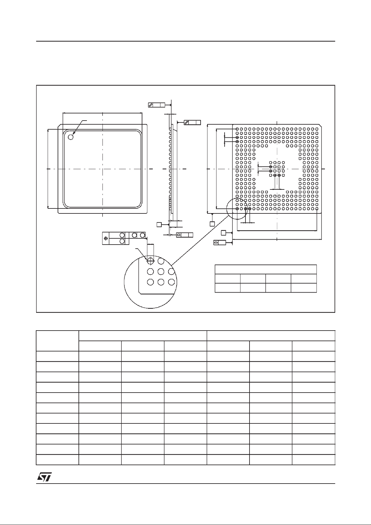
128-BIT 3D MULTIMEDIA ACCELERATOR RIVA128ZX
14 PACKAGE DIMENSION SPECIFICATION
14.1 300 PIN BALL GRID ARRAY PACKAGE
Figure 69. RIVA128ZX 300 Plastic Ball Grid Array Package dimension reference
0.250
D2
Pin 1 indicator
E2
S
0.300 C A B
0.100
SOLDER BALL (Typ)
SS
S
C
C
A1
0.350 C
E
E1
A2
C
b
A
0.150 C
B
(4x)
20 19 18 17 16 15 14 13 12 11 10 9 8 7 6 5 4 3 2 1
e
e
e
A
0.200
D1
D
A
B
C
D
E
F
G
H
J
K
L
M
N
e
P
R
T
U
V
W
Y
All dimensions in mm unless otherwise noted
tolerances unless otherwise noted (mm)
0 ≤ 10 >10 ≤ 50 >50≤ 200 >200
±0.05 ±0.1 ±0.15 ±0.25
Table 25. RIVA128ZX 300 Plastic Ball Grid Array Package dimension specification
Millimeters Inches
Ref.
Typ. Min. Max. Typ. Min. Max.
A 2.125 2.595 0.083 0.102
A1 0.50 0.70 0.020 0.027
A2 1.625 1.895 0.064 0.074
b 0.60 0.90 0.024 0.035
D 27.00 26.82 27.18 1.063 1.055 1.070
D1 24.13 Basic 0.951 Basic
D2 23.90 24.10 0.941 0.949
e 1.27 Basic 0.050 Basic
E 27.00 26.82 27.18 1.063 1.055 1.070
E1 24.13 Basic 0.951 Basic
E2 23.90 24.10 0.941 0.949
67/85
Page 68

128-BIT 3D MULTIMEDIA ACCELERATORRIVA128ZX
15 REFERENCES
1 RIVA128ZX
2 RIVA128ZX
Turnkey Manufacturing Package TMP, Design Guide
Programming Reference Manual,
NVIDIA Corp./STMicroelectronics
3 Accelerated Graphics Port Interface Specification, Revision 1.0
4
PCI Local Bus Specification, revision 2.1
, PCI Special Interest Group, June 1995
5 Recommendation 656 of the CCIR, Interfaces for digital component video signals in 525-line and 625-
line television systems
Display Data Channel (DDC) standard, Version 2.0, revision 0
6
, CCIR, 1990
ation, April 9th 1996 (Video Electronics Standards Association - http://www.vesa.org)
7
AD722 PAL/NTSC TV Encoder Datasheet
8
MK2715 NTSC/PAL Clock Source Datasheet
, Analog Devices Inc., 1995
, MicroClock Inc., March 1997
16 ORDERING INFORMATION
Device Package Supply format Part number
RIVA128ZX 300 pin PBGA Trays STG3005A2S
RIVA128ZX 300 pin PBGA Tapeand reel STG3005A2S/TR
, NVIDIA Corp./STMicroelectronics
, Intel Corporation,July 1996
, Video Electronics Standards Associ-
68/85
Page 69
128-BIT 3D MULTIMEDIA ACCELERATOR RIVA128ZX
APPENDIX
Descriptions of register contents includean indication ifregister fields arereadable
(I)
the initial power-on or reset value of the field
I=X
terminate value, hence
indicates register or field not reset.
. ‘-’ indicates not readable / writable,Xindicates an inde-
(R)
or writable
(W)
and
A PCI CONFIGURATION REGISTERS
This sectiondescribes the 256 byte PCIconfiguration spaces as implementedby theRIVA128ZX. Asingle
PCI VGA deviceis defined by the RIVA128ZX whichdecodes and acknowledges the first 256 bytes of the
configuration addressspace. The RIVA128ZXdoes not respond(does not assertDEVSEL#)for functions
1-7.
A.1 REGISTER DESCRIPTIONS FOR PCI CONFIGURATION SPACE
Byte offsets 0x03 - 0x00
0x03 0x02 0x01 0x00
313029282726252423222120191817161514131211109876543210
DEVICE_ID_CHIP
VENDOR_ID
Device Identification Register (0x03 - 0x02)
Bits Function RWI
31:16 The DEVICE_ID_CHIP bits contain the chip number allocated by the manu-
facturer to identify the particular device.
= 0x0018 if the power-on reset configurationAPCI Supported bit = 0
= 0x0019 if the power-on reset configurationAPCI Supported bit = 1
Vendor Identification Register (0x01 - 0x00)
Bits Function RWI
15:0 VENDOR_ID bits allocated by the PCI Special Interest Group to uniquely
identify the manufacturer of the device.
NVIDIA/STMicroelectronics Vendor ID = 0x12D2 (4818)
R-X
R-X
69/85
Page 70
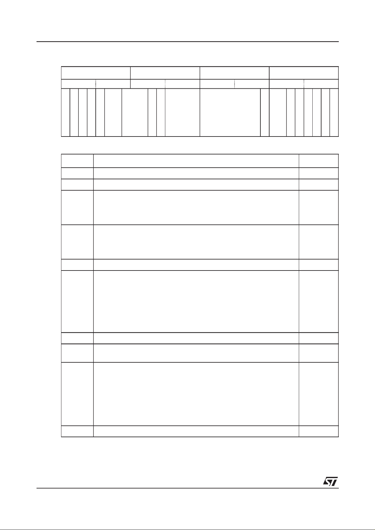
Byte offsets 0x07 - 0x04
0x07 0x06 0x05 0x04
313029282726252423222120191817161514131211109876543210
Reserved
SERR_SIGNALLED
RECEIVED_MASTER
RECEIVED_TARGET
Reserved
DEVSEL_TIMING
Device Status Register (0x07 - 0x06)
Bits Function RWI
31 Reserved R-0
30 SERR_SIGNALLED is set wheneverthe RIVA128ZX assertsSERR#. R W 0
Reserved
66MHZ
CAP_LIST
128-BIT 3D MULTIMEDIA ACCELERATORRIVA128ZX
Reserved
Reserved
SERR_ENABLE
Reserved
PALETTE_SNOOP
WRITE_AND_INVA:
Reserved
BUS_MASTER
MEMORY_SPACE
IO_SPACE
29 RECEIVED_MASTER indicates that a master device’s transaction (except for
RW0
Special Cycle) was terminated with a master-abort. This bit is clearable (=1).
0=No abort
1=Master aborted
28 RECEIVED_TARGET indicates that a master device’s transaction was termi-
RW0
nated with a target-abort. This bitis clearable (=1).
0=No abort
1=Master received target aborted
27 Reserved R-0
26:25 The DEVSEL_TIMING bits indicate the timing of DEVSEL#. These bits indi-
R-1
cate the slowest time that the RIVA128ZX asserts DEVSEL# for any bus
command except Configuration Read and Configuration Write. The
RIVA128ZX responds with medium DEVSEL# for VGA, memory and I/O
accesses. For accesses to the 16MByte memory ranges described by the
BARs, the chip responds with fast decode(no wait states).
00=fast
01=medium
24:22 Reserved R-0
21 66MHZ indicates that theRIVA128ZX is capableof 66MHz operation. This bit
R-1
reflects the latched state of the 66MHz/33MHz strap option.
20 CAP_LIST indicates that there is a linked list of registers containing informa-
R-X
tion about new capabilities not available within the original PCI configuration
structure. This bit indicates that the (byte) Capability Pointer Register located
at 0x34 points to the start of this linked list.
The value of CAP_LIST depends on the RIVA128ZX power-on reset configuration Host Interface and ACPI Supportedsettings:
0 = HostInterface is PCI and ACPI not supported
1= Host interfaceis AGP or ACPI supported
70/85
19:16 Reserved R-0
Page 71

128-BIT 3D MULTIMEDIA ACCELERATOR RIVA128ZX
Command Register (0x05 - 0x04)
Bits Function RWI
15:9 Reserved R-0
8 SERR_ENABLE is an enable bit for the SERR# driver.
0=Disables the SERR# driver
1=Enables the SERR# driver
7:6 Reserved R-0
5 PALETTE_SNOOP indicates that VGA compatible devices shouldsnoop their
palette registers.
0=Palette accesses treatedlike all other accesses
1=Enables special palettesnooping behavior
4 WRITE_AND_INVAL is an enable bit for using the Memory Write and Invali-
date command.
1=The RIVA128ZX as bus master may generate the command
0=The Memory Write command must be used instead of Memory Write and
Invalidate
3 Reserved R-0
2 BUS_MASTER indicates that the device can actas a master on the PCI bus.
0=Disables the RIVA128ZX from generating PCIaccesses
1=Allows the RIVA128ZX to behave as a bus master
1 MEMORY_SPACE indicates that the RIVA128ZX will respond to memory
space accesses.
0=Device response disabled
1=Enables response to Memory space accesses. The device will decode and
respond to the 16MByte ranges as well as the default VGA memory range
when it is enabled. The VGA decode range may change based upon the
value in the VGA graphics Miscellaneous Register GR06, bits[3:2] and other
enable bits, see RIVA128ZX
Programming Reference Manual
[2].
RW0
RW0
RW0
RW0
RW0
0 IO_SPACE indicates that the device will respond to I/O space accesses. This
bit enables I/O space accesses for the VGA function as defined in the PCI
specification. Theseinclude 0x3B0- 0x3BB, 0x3C0- 0x3DFand their aliases.
RW0
71/85
Page 72
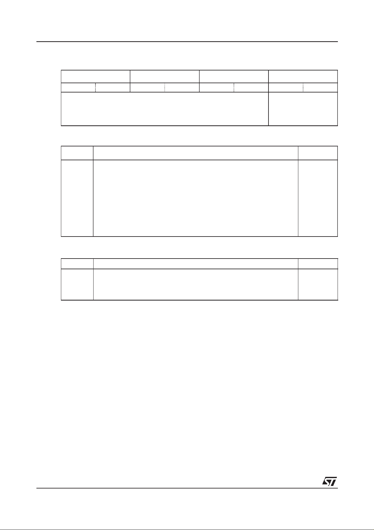
Byte offsets 0x0B - 0x08
0x0B 0x0A 0x09 0x08
128-BIT 3D MULTIMEDIA ACCELERATORRIVA128ZX
313029282726252423222120191817161514131211109876543210
Class Code Register (0x0B - 0x09)
Bits Function RWI
31:8 The CLASS_CODE bits identify the generic function of the device and (in
some cases) a specific register-level programming interface. The register is
broken into three byte-size fields. The upper byte (at offset 0x0B) is a base
class code which broadly classifies the type of function the device performs.
The middle-byte (at offset 0x0A) is a sub-class code which identifies more
specifically thefunction ofthe device.The lowerbyte (at offset 0x09) identifies
a specific register-level programming interface (if any) so thatdevice independent software can interact with the device.
The VGA function responds as a VGA compatible controller.
0x030000=VGA compatible controller
Revision Identification Register (0x08)
Bits Function RWI
7:0 The REVISION_ID bits specify a device specificrevision identifier. The value
is chosen by the vendor.This field should be viewed as a vendor defined
extension to the DEVICE_ID.
0x01=Revision B
CLASS_CODE
REVISION_ID
R-X
R-X
72/85
Page 73
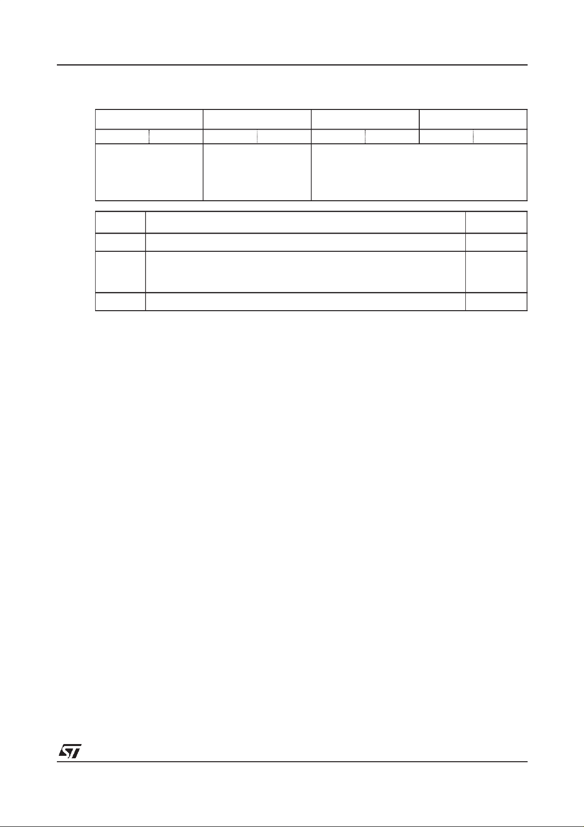
128-BIT 3D MULTIMEDIA ACCELERATOR RIVA128ZX
Byte offsets 0x0F - 0x0C
0x0F 0x0E 0x0D 0x0C
313029282726252423222120191817161514131211109876543210
Reserved
HEADER_TYPE
Reserved
Bits Function RWI
31:24 Reserved R-0
23:16 HEADER_TYPE identifies the device as single or multi-function. RIVA128ZX
R - 0x00
responds as a single-function device.
0x00=Single function device
16:00 Reserved R-0
73/85
Page 74
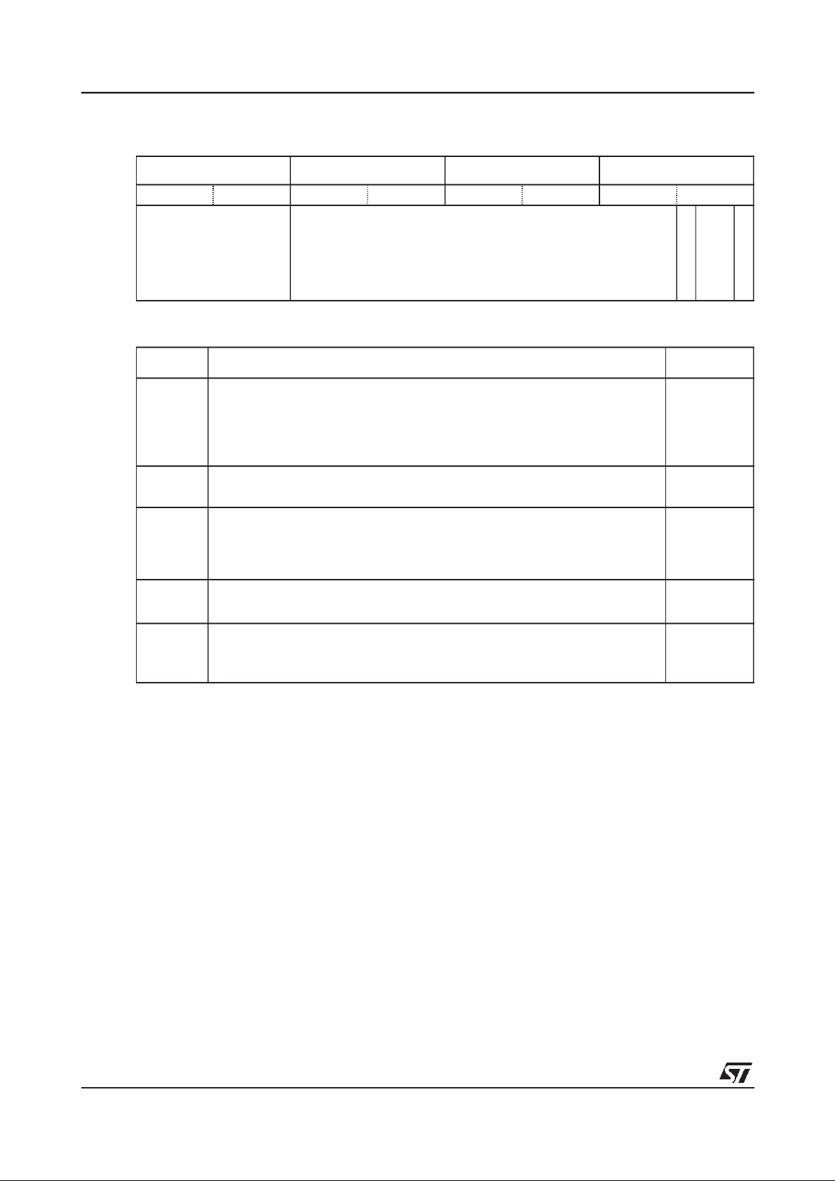
Byte offsets 0x13 - 0x10
0x13 0x12 0x11 0x10
128-BIT 3D MULTIMEDIA ACCELERATORRIVA128ZX
313029282726252423222120191817161514131211109876543210
BASE_ADDRESS
Base Memory Address Register (0x13 - 0x10)
Bits Function RWI
31:24 The BASE_ADDRESS bits contain the most significant bits of the base
address of the device. This indicates that the RIVA128ZX requires a 16MByte
block of contiguous memory beginning on a 16MByte boundary. This memory
range contains memory-mapped registers and FIFOs and should not be set
as part of a PentiumPro’s writecombining range.
23:4 The BASE_RESERVED bitsformthe leastsignificant bitsof the base address
and are hardwired to 0.
3 The PREFETCHABLE bit indicates that there are no side effects on reads,
that the device returns all bytes on reads regardless of the byte enables, and
that host bridges can merge processor writes into this range without causing
errors.
2:1 The ADDRESS_TYPE bits contain the type (width) of the Base Address.
0=32-bit
BASE_RESERVED
PREFETCHABLE
ADDRESS_TYPE
SPACE_TYPE
RW0
R-0
R-1
R-0
0 The SPACE_TYPE bit indicates whetherthe register maps into Memory or I/O
space.
0=Memory space
R-0
74/85
Page 75
128-BIT 3D MULTIMEDIA ACCELERATOR RIVA128ZX
Byte offsets 0x17 - 0x14
0x17 0x16 0x15 0x14
313029282726252423222120191817161514131211109876543210
BASE_ADDRESS
Base Memory Address Register (0x17 - 0x14)
Bits Function RWI
31:24 The BASE_ADDRESS bits contain the most significant bits of the base
address of the device. This indicates that the RIVA128ZX requires a 16MByte
block of contiguous memory beginning on a 16MByte boundary. This memory
range contains linear frame buffer access and may be set as part of a PentiumPro’s write combining (wc) range.
23:4 The BASE_RESERVED bitsformthe leastsignificant bitsof the base address
and are hardwired to 0.
3 The PREFETCHABLE bit indicates that there are no side effects on reads,
that the device returns all bytes on reads regardless of the byte enables, and
that host bridges can merge processor writes into this range without causing
errors.
2:1 The ADDRESS_TYPE bits contain the type (width) of the Base Address.
0=32-bit
BASE_RESERVED
PREFETCHABLE
ADDRESS_TYPE
SPACE_TYPE
RW0
R-0
R-1
R-0
0 The SPACE_TYPE bit indicates whetherthe register maps into Memory or I/O
space.
0=Memory space
Byte offsets 0x2B - 0x18
313029282726252423222120191817161514131211109876543210
Base Address Registers (0x2B - 0x18)
Bits Function RWI
31:0 These bits are hardwired (read-only) to 0. R -0
R-0
0x00000000
75/85
Page 76
Byte offsets 0x2F - 0x2C
0x2F 0x2E 0x2D 0x2C
128-BIT 3D MULTIMEDIA ACCELERATORRIVA128ZX
313029282726252423222120191817161514131211109876543210
SUBSYSTEM_ID
Subsystem Vendor ID (0x2F - 0x2C)
Bits Function RWI
31:16 SUBSYSTEM_ID is a unique code defined by the vendor to identify this prod-
uct.
15:0 SUB_VENDOR_ID bits allocated by the PCI Special Interest Group to
uniquely identify the manufacturer of the sub-system. Based on the strapping
options read from ROM during PCI reset, this field may behave in one of two
ways:
1 These bytes can be read from address locations 0x54 - 0x57 of the ROM
BIOS automatically during reset.This is useful for add-in card implementations.
2 These bytesmay bewrittenfrom PCI configuration spaceat locations 0x40
- 0x43.
SUB_VENDOR_ID
R-0
R-0
76/85
Page 77
128-BIT 3D MULTIMEDIA ACCELERATOR RIVA128ZX
Byte offsets 0x33 - 0x30
0x33 0x32 0x31 0x30
313029282726252423222120191817161514131211109876543210
ROM_BASE_ADDRESS
Expansion ROM Base Address Register (0x33 - 0x30)
Bits Function RWI
31:22 The ROM_BASE_ADDR bits contain the base address of the Expansion
ROM. The bits correspond to the upper bits of the Expansion ROM base
address. This decode permits the PCI boot manager to place the expansion
ROM on a 4MByte boundary. RIVA128ZX currently maps a 64KByte BIOS
into the bottom of this 4MByte range.Typically the first 32K of this ROM contains the VGA BIOS code as well as the PCI BIOS Expansion ROM Header
and Data Structure.
21:11 ROM_BASE_RESERVED contain the lower bits of the base address of the
Expansion ROM. These bits are hardwired to 0, forcing a 4MByte boundary.
10:1 Reserved R-0
ROM_BASE_RESERVED
Reserved
ROM_DECODE
RWX
R-0
0 The ROM_DECODE bit indicates whether or not the RIVA128ZX accepts
accesses to its expansion ROM. When the bit is set, address decoding is
enabled using the parameters in the other part of the base register. The
MEMORY_SPACE bit (PCI Configuration Register 0x04, page 70) has precedence over the ROM_DECODE bit. RIVA128ZX will respond to accesses to
its expansion ROM only if both the MEMORY_SPACE bit and the
ROM_DECODE bit are set to 1.
0=Expansion ROM address space is disabled
1=Expansion ROM address decoding is enabled
RW0
77/85
Page 78
Byte offsets 0x37 - 0x34
0x37 0x36 0x35 0x34
128-BIT 3D MULTIMEDIA ACCELERATORRIVA128ZX
313029282726252423222120191817161514131211109876543210
Capabilities Pointer Register (0x37 - 0x34)
Bits Function RWI
31:8 Reserved R-0
7:0 This field contains a byte offset into this PCI configuration space containing
the first item in the capabilities list. The offset returned depends on the
RIVA128ZX power-on reset configuration Host Interface and ACPI Supported
settings:
CAP_PTR = 0x0 if Host Interface is PCI and APCI not supported
CAP_PTR = 0x44 if Host Interface is AGP and APCInot supported
CAP_PTR = 0x60 if APCI supported
Byte offsets 0x3B - 0x38
313029282726252423222120191817161514131211109876543210
Reserved
CAP_PTR
R-X
0x00000000
Reserved (0x3B - 0x38)
Bits Function RWI
31:0 These bits are reserved and hardwired (read-only) to 0. R - 0
78/85
Page 79
128-BIT 3D MULTIMEDIA ACCELERATOR RIVA128ZX
Byte offset 0x3F - 0x3C
0x3F 0x3E 0x3D 0x3C
313029282726252423222120191817161514131211109876543210
MAX_LAT
MAX_LAT Register (0x3F)
Bits Function RWI
31:24 The MAX_LAT bits contain the maximum time the RIVA128ZX requires to
gain access to the PCI bus. This read-only register is used to specify the
RIVA128ZX’s desiredsettings forLatency Timervalues. Thevalue specifiesa
period of time in units of 250ns.
1=250ns
MIN_GNT Register (0x3E)
Bits Function RWI
23:16 The MIN_GNT bits contain the length of the burst period the RIVA128ZX
needs, assuming a clock rate of 33MHz. This read-only register is used to
specify theRIVA128ZX’s desiredsettings forLatency Timer values. The value
specifies a period of time in units of 250ns.
3=750ns
MIN_GNT
INTERRUPT_PIN
INTERRUPT_LINE
R-1
R-3
Interrupt Pin Register (0x3D)
Bits Function RWI
15:8 The INTERRUPT_PIN bitscontain the interruptpin the device (or device func-
tion) uses. A value of 1 corresponds to INTA#.
Interrupt Line Register (0x3C)
Bits Function RWI
7:0 The INTERRUPT_LINE bits contain the interrupt routing information. POST
software will write the routing information into this register as it initializes and
configures the system. The value in this field indicates which input of the system interrupt controller(s) the RIVA128ZX’s interrupt pin is connected to.
Device drivers and operating systems can use this information to determine
priority and vector information. INTERRUPT_LINE is initialized to 0xFF (no
connection) at reset.
0=Interrupt line IRQ0
1=Interrupt line IRQ1
0xF=Interrupt line IRQ15
0xFF=No interrupt line connection (reset value)
R-1
R W 0xFF
79/85
Page 80
Byte offsets 0x43 - 0x40
0x43 0x42 0x41 0x40
128-BIT 3D MULTIMEDIA ACCELERATORRIVA128ZX
313029282726252423222120191817161514131211109876543210
SUBSYSTEM_ID
Writeable Subsystem Vendor ID (0x43 - 0x40)
Bits Function RWI
31:16 This SUBSYSTEM_ID field is aliased at 0x2F - 0x2E where it is read-only. It
may be modified by System BIOS for systems which do not have a ROM on
the RIVA128ZX data pins. This will ensure valid data before enumeration by
the operating system.
15:0 This SUB_VENDOR_ID fieldis aliasedat 0x2D - 0x2C where it is read-only. It
may be modified by System BIOS for systems which do not have a ROM on
the RIVA128ZX data pins. This will ensure valid data before enumeration by
the operating system.
Byte offsets 0x47 - 0x44
0x47 0x46 0x45 0x44
SUB_VENDOR_ID
RW0
RW0
313029282726252423222120191817161514131211109876543210
Reserved
MAJOR
MINOR
Capabilities Identifier Register (Offset = 0x47 - 0x44 = CAP_PTR)
Bits Function RWI
31:24 Reserved = 0x00 R - 0
23:20 This field indicates the Major revision number of the AGP specification that
the RIVA128ZX conforms to.
= 0x01
19:16 This field indicates the Minor revision number of the AGP specification that
the RIVA128ZX conforms to.
= 0x00
15:8 NEXT_PTR contains the pointer to the next item in the capabilities list. This is
the last entry in the capabilities list, hence it contains a null pointer = 0x00.
7:0 The CAP_ID field identifies the type of capability.
AGP = 0x02
NEXT_PTR
CAP_ID
R - 0x01
R - 0x00
R - 0x00
R - 0x02
80/85
Page 81
128-BIT 3D MULTIMEDIA ACCELERATOR RIVA128ZX
Byte offsets 0x4B - 0x48
0x4B 0x4A 0x49 0x48
313029282726252423222120191817161514131211109876543210
RQ
AGP Status Register (0x4B - 0x48 = CAP_PTR+4)
Bits Function RWI
31:24 The RQ field contains the maximum number of AGP command requests this
device can have outstanding.
RQ = 0x04
23:10 Reserved R-0
9 SBA indicates whether the RIVA128ZX supports sideband addressing.
0 = Sidebandaddressing not supported
8:2 Reserved R-0
1:0 RATE indicates the data transfer rate(s) supportedby the RIVA128ZX.
11 = 66MHz 1x supported; 133MHz 2x supported
Reserved
SBA
Reserved
RATE
R - 0x04
R-0
R - 0x11
81/85
Page 82

Byte offsets 0x4F - 0x4C
0x4F 0x4E 0x4D 0x4C
128-BIT 3D MULTIMEDIA ACCELERATORRIVA128ZX
313029282726252423222120191817161514131211109876543210
RQ_DEPTH
Reserved
AGP Command Register (0x4F - 0x4C = CAP_PTR + 8)
Bits Function RWI
31:24 This field is set to the minimum request depth of the target as reported in its
RQ field.
23:10 Reserved R-0
9 SBA_ENABLE enables sideband addressing when set. The RIVA128ZX does
not implement sidebandaddressing.
8 AGP_ENABLE allows the RIVA128ZX to act as an AGP master and initiate
AGP operations. The target must be enabled before enablingthe RIVA128ZX
0 = disabled
1 = AGP operations enabled
7:3 Reserved R-0
2:0 The DATA_RATE field must be set to 0x01 to indicate 66MHz/1x transfer
mode or 0x02 for 133MHz/2x transfer mode. This value must also be set on
the target before being enabled. The initial value 0x00 indicates PCI operation.
SBA_ENABLE
AGP_ENABLE
Reserved
DATA_RATE
RW-
R-0
RW0
R W 0x00
82/85
Page 83
128-BIT 3D MULTIMEDIA ACCELERATOR RIVA128ZX
Byte offsets 0x63 - 0x60
0x63 0x62 0x61 0x60
313029282726252423222120191817161514131211109876543210
Reserved
VERSION
Power Management Capabilities Register (0x63 - 0x60)
Bits Function RWI
31:19 Reserved R-0
18:16 VERSION indicates that RIVA128ZX is compliant with Revision 1.0 of thePCI
Power Management Interface Specification.
15:8 NEXT_PTR indicates the offset for the next item in the capability list. If the
power-on reset configuration HostInterface bit indicates PCI then NEXT_PTR
will be null (0x00), indicating there are no further items. If the power-on reset
configuration indicates AGP then NEXT_PTR will indicate the next item’s offset (the AGP capability, 0x44).
7:0 A value of ‘1’ read back from CAP_ID indicatesthis is the PowerManagement
Register.
NEXT_PTR
CAP_ID
R-1
R-X
R-1
83/85
Page 84
Byte offsets 0x67 - 0x64
0x67 0x66 0x65 0x64
128-BIT 3D MULTIMEDIA ACCELERATORRIVA128ZX
313029282726252423222120191817161514131211109876543210
Reserved
Power Management Control/Status Register (0x67 - 0x64)
Bits Function RWI
31:2 Reserved R-0
1:0 POWER_STATE indicates and controls the current power state of
RIVA128ZX. Two power states are supported D0 (full power) and D3hot (low
power).
0x0 = D0
0x3 = D3hot
The RIVA128ZX does not physically change its power consumption when
POWER_STATE is modified. The device can be transitioned from D3 to D0
either by writing to this register or by applying a hard reset to the PCIRST#
pin.
Byte offset 0xFF - 0x50
POWER_STATE
RW0
313029282726252423222120191817161514131211109876543210
Reserved = 0x00000000
84/85
Page 85

128-BIT 3D MULTIMEDIA ACCELERATOR RIVA128ZX
85
Information furnishedis believed to be accurate and reliable. However, STMicroelectronics assumesno responsibility for the consequences
of use of such information nor for any infringement of patents or otherrights of third partieswhich may result from itsuse.No license isgranted
by implication orotherwise under any patent or patent rights of STMicroelectronics. Specifications mentioned in this publication are subject
to change without notice. This publication supersedes and replaces all information previously supplied. STMicroelectronicsproducts are not
authorized for use as critical components in life support devices or systems without express written approval of STMicroelectronics.
The ST logo is a registered trademark of STMicroelectronics.
.
RIVA 128 and RIVA128ZX are trademarks of STMicroelectronics and NVIDIA Corp.
Microsoft, Windows and the Windows logo are registered trademarks of Microsoft Corporation
All other products mentioned in thisdocument are trademarks or registered trademarks of their respective owners.
1998 STMicroelectronicsInc.
STMicroelectronics GROUP OF COMPANIES
Australia -Brazil - Canada - France - Germany - Italy - Japan - Korea - Malaysia - Malta - Mexico - Morocco - The Netherlands -
Singapore - Spain -Sweden - Switzerland - Taiwan - Thailand - United Kingdom -U.S.A.
Document number: 7071857 00
85/85
 Loading...