

Page 1
RHRU10060
Data Sheet January 2000 File Number 3572.3
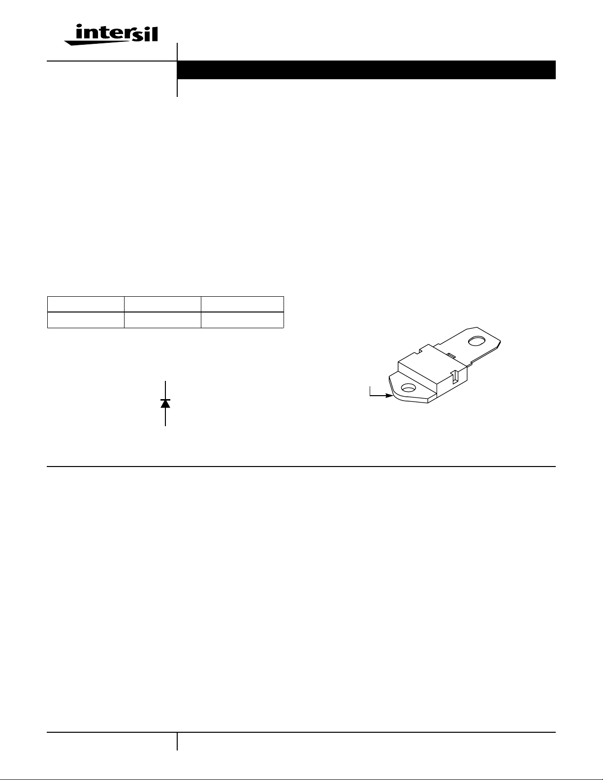
100A, 600V Hyperfast Diode
The RHRU10060 is a hyperfast diode with soft recovery
characteristics (t
< 50ns). It has half the recovery time of
rr
ultrafast diodes and is of silicon nitride passivated
ion-implanted epitaxial planar construction.
This device is intended for use as a freewheeling/clamping
diode and rectifier in a variety of switching power supplies
and other powerswitchingapplications.Itslow stored charge
and hyperfast soft recovery minimize ringing and electrical
noise in many power switching circuits, thus reducing power
loss in the switching transistors.
Formerly developmental type TA49069.
Ordering Information
PART NUMBER PACKAGE BRAND
RHRU10060 TO-218 RHRU10060
NOTE: When ordering, use the entire part number.
Symbol
K
Features
• Hyperfast with Soft Recovery. . . . . . . . . . . . . . . . . < 50ns
• Operating Temperature. . . . . . . . . . . . . . . . . . . . . . .175
o
• Reverse Voltage. . . . . . . . . . . . . . . . . . . . . . . . . . . . .600V
• Avalanche Energy Rated
• Planar Construction
Applications
• Switching Power Supplies
• Power Switching Circuits
• General Purpose
Packaging
JEDEC STYLE TO-218
ANODE
CATHODE
(FLANGE)
C
A
Absolute Maximum Ratings T
Peak Repetitive Reverse Voltage. . . . . . . . . . . . . . . . . . . . . . . . . . . . . . . . . . . . . . . . . . . V
Working Peak Reverse Voltage . . . . . . . . . . . . . . . . . . . . . . . . . . . . . . . . . . . . . . . . . . . . V
DC Blocking Voltage . . . . . . . . . . . . . . . . . . . . . . . . . . . . . . . . . . . . . . . . . . . . . . . . . . . . . . .V
Average Rectified Forward Current . . . . . . . . . . . . . . . . . . . . . . . . . . . . . . . . . . . . . . . . . .I
(TC = 60oC)
Repetitive Peak Surge Current . . . . . . . . . . . . . . . . . . . . . . . . . . . . . . . . . . . . . . . . . . . . . I
(Square Wave, 20kHz)
Nonrepetitive Peak Surge Current. . . . . . . . . . . . . . . . . . . . . . . . . . . . . . . . . . . . . . . . . . . I
(Halfwave, 1 Phase, 60Hz)
Maximum Power Dissipation . . . . . . . . . . . . . . . . . . . . . . . . . . . . . . . . . . . . . . . . . . . . . . . . . P
Avalanche Energy (See Figures 7 and 8) . . . . . . . . . . . . . . . . . . . . . . . . . . . . . . . . . . . . . E
Operating and Storage Temperature . . . . . . . . . . . . . . . . . . . . . . . . . . . . . . . . . . . . . . T
= 25oC
C
STG
RRM
RWM
F(AV)
FRM
FSM
AVL
, T
RHRU10060 UNITS
600 V
600 V
R
D
J
600 V
100 A
200 A
1000 A
210 W
50 mJ
-65 to 175
o
C
1
1-888-INTERSIL or 321-724-7143 | Copyright © Intersil Corporation 2000
Page 2
RHRU10060
Electrical Specifications T
= 25oC, Unless Otherwise Specified
C
SYMBOL TEST CONDITION MIN TYP MAX UNITS
V
F
IF = 100A - - 2.1 V
IF = 100A, TC = 150oC - - 1.7 V
I
R
VR = 600V - - 250 µA
VR = 600V, TC = 150oC - - 2.0 mA
t
rr
IF = 1A, dIF/dt = 100A/µs- - 50 ns
IF = 100A, dIF/dt = 100A/µs- - 60 ns
t
a
t
b
R
θJC
IF = 100A, dIF/dt = 100A/µs - 28 - ns
IF = 100A, dIF/dt = 100A/µs - 18 - ns
- - 0.71
DEFINITIONS
VF = Instantaneous forward voltage (pw = 300µs, D = 2%).
IR = Instantaneous reverse current.
trr= Reverse recovery time (See Figure 6), summation of ta+tb.
ta = Time to reach peak reverse current (See Figure 6).
tb = Time from peak IRM to projected zero crossing of IRM based on a straight line from peak IRM through 25% of IRM (See Figure 6).
R
= Thermal resistance junction to case.
θJC
pw = pulse width.
D = duty cycle.
o
C/W
Typical Performance Curves
500
175oC
100
100oC
10
, FORWARD CURRENT (A)
F
I
1
0
0.5 1
VF, FORWARD VOLTAGE (V)
25oC
1.5 2.5 32
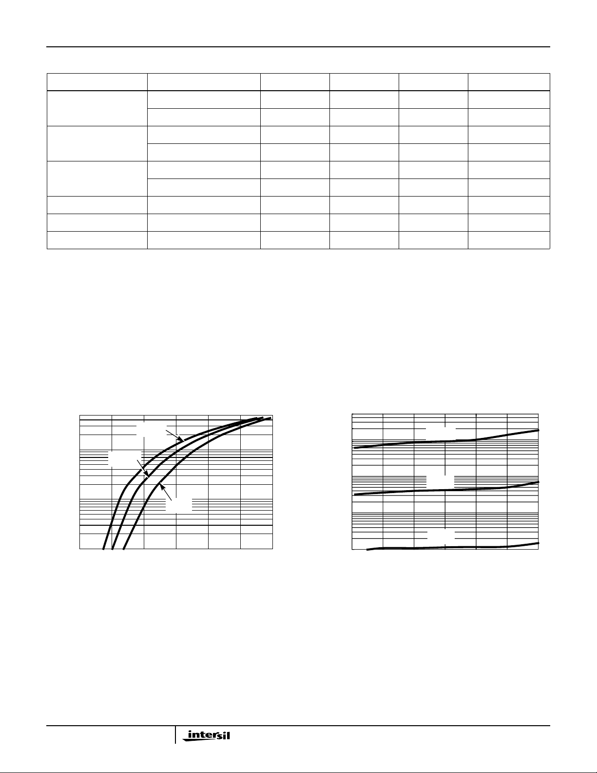
FIGURE 1. FORWARD CURRENT vs FORWARD VOLTAGE FIGURE 2. REVERSE CURRENT vs REVERSE VOLTAGE
, REVERSE CURRENT (µA)
I
R
5000
1000
100
175oC
100oC
10
25oC
1
1000
200 300
VR, REVERSE VOLTAGE (V)
400 600500
2
Page 3
Typical Performance Curves (Continued)
RHRU10060
60
50
40
30
20
t, RECOVERY TIMES (ns)
10
0
TC = 25oC, dIF/dt = 100A/µs
t
rr
t
a
t
b
101
IF, FORWARD CURRENT (A)
100
120
100
80
60
40
20
, AVERAGE FORWARD CURRENT (A)
F(AV)
I
0
25
50 75
DC
SQ. WAVE
100
TC, CASE TEMPERATURE (oC)
125
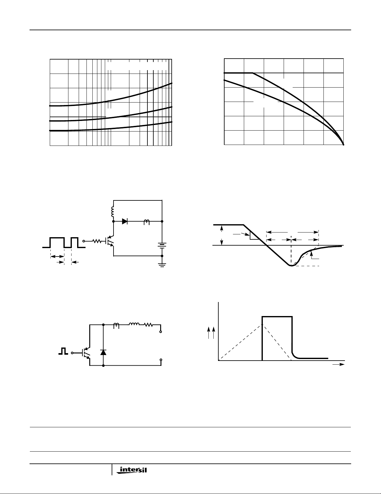
FIGURE 3. trr,taAND tbCURVES vs FORWARD CURRENT FIGURE 4. CURRENT DERATING CURVE
Test Circuits and Waveforms
VGE AMPLITUDE AND
RG CONTROL dIF/dt
t
V
GE
1 ANDt2
CONTROL I
t
1
F
R
t
2
L
DUT
CURRENT
G
IGBT
SENSE
+
V
DD
-
0
dI
F
I
F
dt
t
rr
t
a
t
b
150 175
0.25 I
RM
I
RM
FIGURE 5. trr TEST CIRCUIT FIGURE 6. trr WAVEFORMS AND DEFINITIONS
I
= 1.6A
MAX
L = 40mH
R < 0.1Ω
E
AVL
= IGBT (BV
Q
1
= 1/2LI2 [V
R(AVL)
CES
/(V
> DUT V
Q
R(AVL)
R(AVL)
1
- VDD)]
)
CURRENT
DUT
SENSE
LR
+
V
V
-
DD
DD
IV
V
AVL
I
L
t
0
I
L
t
1
t
2
t
FIGURE 7. AVALANCHE ENERGY TEST CIRCUIT FIGURE 8. AVALANCHECURRENT AND VOLTAGE
WAVEFORMS
All Intersil semiconductor products are manufactured, assembled and tested under ISO9000 quality systems certification.
Intersil semiconductor products are sold by description only. Intersil Corporation reserves the right to make changes in circuit design and/or specifications at any time without notice. Accordingly, the reader is cautioned to verify that data sheets are current before placing orders. Information furnished by Intersil is believed to be accurate and
reliable. However, no responsibility is assumed by Intersil or its subsidiaries for its use; nor for any infringements of patents or other rights of third parties which may result
from its use. No license is granted by implication or otherwise under any patent or patent rights of Intersil or its subsidiaries.
For information regarding Intersil Corporation and its products, see web site www.intersil.com
3
 Loading...