

Page 1
RHR1K160
Data Sheet January 2000
1A, 600V Hyperfast Diode
The RHR1K160 is a hyperfast diode with soft recovery
characteristics (t
< 25ns). It has half the recovery time of
rr
ultrafast diodes and is silicon nitride passivated ionimplanted epitaxial planar construction.
This device is intended for use as freewheeling/clamping
diodes and rectifiers in a variety of switching power supplies
and otherpowerswitching applications. Its low stored charge
and hyperfast soft recovery minimize ringing and electrical
noise in many power switching circuits reducing power loss
in the switching transistors.
Formerly developmental type TA49185.
Ordering Information
PART NUMBER PACKAGE BRAND
RHR1K160 MS-012AA RHR1K160
NOTE: When ordering, use the entire partn umber. For ordering in tape
and reel, add the suffix 96 to the part number, i.e. RHR1K16096.
File Number 4789
Features
• Hyperfast with Soft Recovery. . . . . . . . . . . . . . . . . .<25ns
• Operating Temperature. . . . . . . . . . . . . . . . . . . . . . .150
o
• Reverse Voltage . . . . . . . . . . . . . . . . . . . . . . . . . . . . .600V
• Thermal Impedance SPICE Model
• Thermal Impedance SABER™ Model
• Avalanche Energy Rated
• Planar Construction
• Related Literature
- TB334, “Guidelines for Soldering Surface Mount
Components to PC Boards”
Applications
• Switching Power Supplies
• Power Switching Circuits
• General Purpose
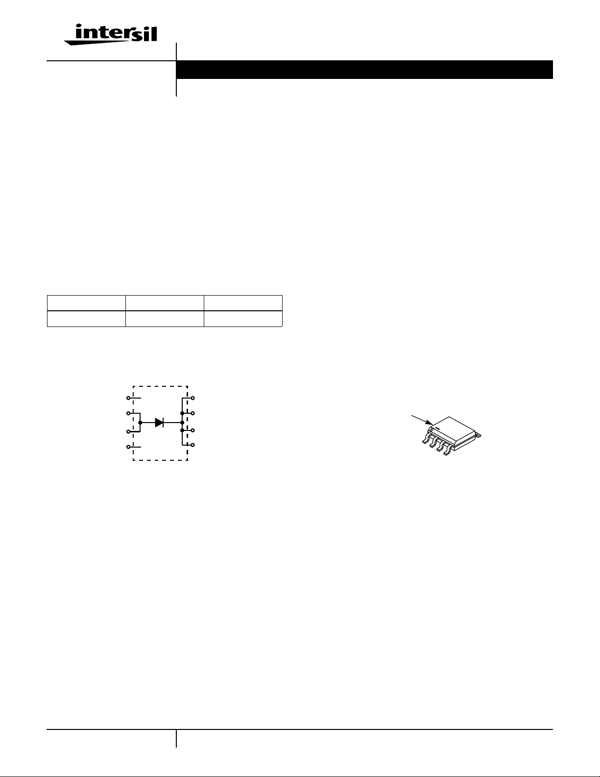
C
Symbol
NC (1)
ANODE (2)
ANODE (3)
NC (4)
Absolute Maximum Ratings T
Peak Repetitive Reverse Voltage. . . . . . . . . . . . . . . . . . . . . . . . . . . . . . . . . . . . . . . . . . . V
Working Peak Reverse Voltage . . . . . . . . . . . . . . . . . . . . . . . . . . . . . . . . . . . . . . . . . . . .V
DC Blocking Voltage . . . . . . . . . . . . . . . . . . . . . . . . . . . . . . . . . . . . . . . . . . . . . . . . . . . . . . V
Average Rectified Forward Current . . . . . . . . . . . . . . . . . . . . . . . . . . . . . . . . . . . . . . . . . I
TA = 65oC
Repetitive Peak Surge Current . . . . . . . . . . . . . . . . . . . . . . . . . . . . . . . . . . . . . . . . . . . . .I
Square Wave, 20kHz
Nonrepetitive Peak Surge Current. . . . . . . . . . . . . . . . . . . . . . . . . . . . . . . . . . . . . . . . . . . I
Halfwave, 1 Phase, 60Hz
Maximum Power Dissipation (Note 1) . . . . . . . . . . . . . . . . . . . . . . . . . . . . . . . . . . . . . . . . . P
Avalanche Energy (See Figures 11 and 12) . . . . . . . . . . . . . . . . . . . . . . . . . . . . . . . . . . .E
Operating and Storage Temperature . . . . . . . . . . . . . . . . . . . . . . . . . . . . . . . . . . . . . T
Maximum Temperature for Soldering
Leads at 0.063in (1.6mm) from Case for 10s. . . . . . . . . . . . . . . . . . . . . . . . . . . . . . . . . . T
Package Body for 10s, See Tech brief 334 . . . . . . . . . . . . . . . . . . . . . . . . . . . . . . . . . .T
CAUTION: Stresses above those listed in “Absolute Maximum Ratings” may cause permanent damage to the device. This is a stress only rating and operation of the
device at these or any other conditions above those indicated in the operational sections of this specification is not implied.
CATHODE (8)
CATHODE (7)
CATHODE (6)
CATHODE (5)
= 25oC, Unless Otherwise Specified
A
Packaging
RRM
RWM
R
F(AV)
FRM
FSM
D
AVL
STG,TJ
L
pkg
JEDEC MS-012AA
BRANDING DASH
1
2
3
4
RHR1K160 UNITS
600 V
600 V
600 V
1A
2A
10 A
2.5 W
5mJ
-55 to 150
300
260
5
o
C
o
C
o
C
3-1
1-888-INTERSIL or 321-724-7143 | Copyright © Intersil Corporation 2000
SABER™ is a Copyright of Analogy, Inc.
Page 2

RHR1K160
Electrical Specifications T
= 25oC, Unless Otherwise Specified
A
SYMBOL TEST CONDITION MIN TYP MAX UNITS
V
F
IF = 1A - - 2.1 V
IF = 1A, TA = 150oC - - 1.7 V
I
R
VR = 600V - - 100 µA
VR = 600V, TA = 150oC - - 500 µA
t
rr
t
a
t
b
Q
RR
C
J
R
θJA
IF = 1A, dIF/dt = 200A/µs--25ns
IF = 1A, dIF/dt = 200A/µs - 10.5 - ns
IF = 1A, dIF/dt = 200A/µs-5-ns
IF = 1A, dIF/dt = 200A/µs - 20 - nC
VR = 10V, IF = 0A - 10 - pF
Pad Area = 0.769 in2(Note 1) - - 50
Pad Area = 0.054 in2(Note 2) (Figure 13) - - 177
Pad Area = 0.0115 in2(Note 2) (Figure 13) - - 217
DEFINITIONS
VF = Instantaneous forward voltage (pw = 300µs, D = 2%).
IR = Instantaneous reverse current.
trr= Reverse recovery time (See Figure 10), summation of ta+tb.
ta = Time to reach peak reverse current (See Figure 10).
tb = Time from peak IRM to projected zero crossing of IRM based on a straight line from peak IRM through 25% of IRM (See Figure 10).
Qrr = Reverse recovery charge.
CJ = Junction Capacitance.
R
= Thermal resistance junction to ambient.
θJA
pw = Pulse width.
D = Duty cycle.
NOTES:
1. Measured using FR-4 copper board at 3.2 seconds.
2. Measured using FR-4 copper board at 1000 seconds.
o
o
o
C/W
C/W
C/W
3-2
Page 3
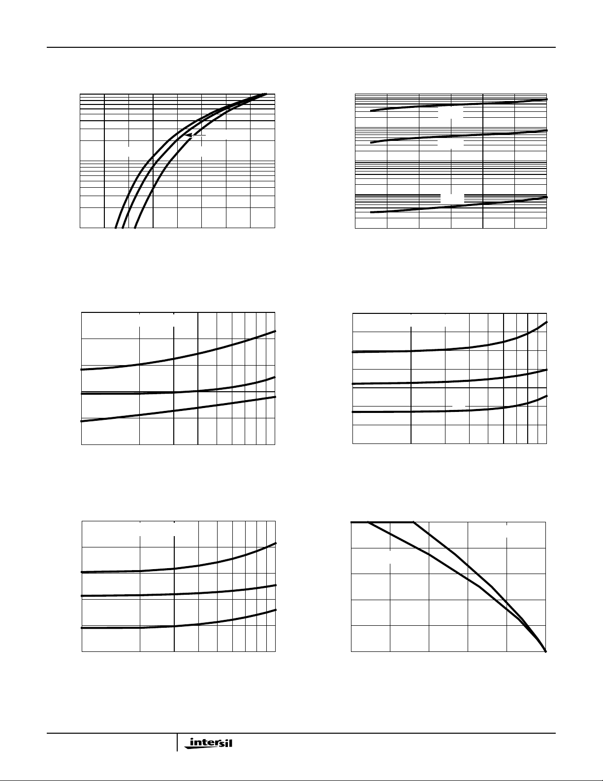
Typical Performance Curves
RHR1K160
10
100oC
1
, FORWARD CURRENT (A)
F
I
0.1
0 0.5 1 1.5 2 2.5 4
150oC
VF, FORWARD VOLTAGE (V)
25oC
3.53
10
1
0.1
REVERSE CURRENT (µA)
0.01
R,
I
0.001
0 600100 500200
o
150
C
o
C
100
25oC
300 400
VR, REVERSE VOLTAGE (V)
FIGURE 1. FORWARD CURRENT vs FORWARD VOLTAGE FIGURE 2. REVERSE CURRENT vs REVERSE VOLTAGE
20
TA = 25oC, dIF/dt = 200A/ sTA = 25oC, dIF/dt = 200A/µs
16
12
8
t, RECOVERY TIMES (ns)
4
t
r
t
a
t
b
35
TA = 100oC, dIF/dt = 200A/µs
30
25
20
15
10
t, RECOVERY TIMES (ns)
5
t
rr
t
b
t
a
0
0.1
IF, FORWARD CURRENT (A)
0.5
1
0
0.1
IF, FORWARD CURRENT (A)
0.5
FIGURE 3. trr,taAND tbCURVES vs FORWARD CURRENT FIGURE 4. trr,taAND tbCURVES vs FORWARD CURRENT
50
TA = 150oC, dIF/dt = 200A/µs
40
30
20
t, RECOVERY TIMES (ns)
10
0
0.1
t
rr
t
b
t
a
0.5
IF, FORWARD CURRENT (A)
1
1.0
0.8
0.6
0.4
0.2
, AVERAGE FORWARD CURRENT (A)
0
F(AV)
I
SQ. WAVE
DC
50 75 12525 150100
, AMBIENT TEMPERATURE (oC)
T
A
R
θJA
= 50oC/W
FIGURE 5. trr,taAND tbCURVES vs FORWARD CURRENT FIGURE 6. CURRENT DERATING CURVE
1
3-3
Page 4

Typical Performance Curves (Continued)
50
40
30
20
10
, JUNCTION CAPACITANCE (pF)
J
C
0
0 20 40 60 10080
FIGURE 7. JUNCTION CAPACITANCE vs REVERSE VOLTAGE
RHR1K160
, REVERSE VOLTAGE (V)
V
R
10
DUTY CYCLE - DESCENDING ORDER
0.5
0.2
0.1
1
0.05
0.02
0.01
, NORMALIZED
0.1
JA
θ
Z
THERMAL IMPEDANCE
0.01
-5
10
SINGLE PULSE
-4
10
10
FIGURE 8. NORMALIZED MAXIMUM TRANSIENT THERMAL IMPEDANCE
Test Circuits and Waveforms
VGE AMPLITUDE AND
RG CONTROL dIF/dt
t
1 ANDt2
CONTROL I
F
L
R
= 50oC/W
θJA
P
DM
t
1
t
JA
1/t2
10
x R
2
2
+ T
JA
A
θ
3
10
NOTES:
DUTY FACTOR: D = t
PEAK TJ = PDM x Z
-3
-2
10
-1
10
0
10
1
10
θ
t, RECTANGULAR PULSE DURATION (s)
DUT
CURRENT
R
G
V
GE
t
1
t
2
IGBT
SENSE
dI
+
V
DD
-
0
F
I
F
dt
t
rr
t
a
t
b
0.25 I
RM
I
RM
FIGURE 9. trr TEST CIRCUIT FIGURE 10. trr WAVEFORMS AND DEFINITIONS
3-4
Page 5

RHR1K160
Test Circuits and Waveforms (Continued)
L = 20mH
R < 0.1Ω
E
AVL
Q
= IGBT (BV
1
= 1/2LI2 [V
Q
CES
1
R(AVL)
> DUT V
/(V
R(AVL)
R(AVL)
CURRENT
SENSE
DUT
- VDD)]
)
LR
V
+
V
DD
I
L
IV
V
DD
-
t
0
AVL
I
L
t
1
t
2
FIGURE 11. AVALANCHE ENERGY TEST CIRCUIT FIGURE 12. AVALANCHE CURRENT AND VOLTAGE
WAVEFORMS
Thermal Resistance vs Mounting Pad Area
The maximum rated junction temperature, TJM, and the
thermal resistance of the heat dissipating path determines
the maximum allowabledevicepower dissipation, P
DM
,inan
application.Therefore the application’s ambient temperature,
T
(oC), and thermal resistance R
A
reviewed to ensure that T
JM
is never exceeded. Equation 1
(oC/W) must be
θJA
mathematically represents the relationship and serves as
the basis for establishing the rating of the part.
P
TJMTA–()
-----------------------------=
DM
Z
θJA
(EQ. 1)
In using surface mount devices such as the SO-8 package,
the environment in which it is applied will have a significant
influence on the part’s current and maximum power
dissipation ratings. Precise determination of the P
DM
is
complex and influenced by many factors:
1. Mounting padarea onto which the device isattached and
whether there is copper on one side or both sides of the
board.
2. The number of copper layers and the thickness of the
board.
3. The use of external heat sinks.
4. The use of thermal vias.
5. Air flow and board orientation.
6. For non steady state applications, the pulse width, the
duty cycle andthe transient thermal response ofthe part,
the board and the environment they are in.
Intersil provides thermal information to assist the designer’s
preliminary application evaluation. Figure 13 defines the
for the device as a function of the top copper
R
θJA
(component side) area. This is for a horizontally positioned
FR-4 board with 2 oz. copper after 1000 seconds of steady
state power with no air flow. This graph provides the
necessary information for calculation of the steady state
junction temperature or power dissipation. Pulse
applications can be evaluated using the Intersil device Spice
thermal model or manually utilizing the normalized maximum
transient thermal impedance curve.
350
300
C/W)
o
250
200
217oC/W - 0.0123in
150
, THERMAL IMPEDANCE
θJA
100
R
JUNCTION TO AMBIENT (
50
0.001
CATHODE MOUNTING AREA, TOP COPPER AREA (in
FIGURE 13. THERMAL RESISTANCEvs MOUNTING PAD
AREA
Displayed on the curve are R
R
= 101.6 - 25.82 x ln(AREA)
θJA
2
0.01
values listed in the
θJA
Electrical Specifications table. These points were chosen to
depict the compromise between the copper board area, the
thermal resistance and ultimately the power dissipation,
P
. Thermal resistances corresponding to other
DM
component side copper areas can be obtained from Figure
13 or by calculation using Equation 2. The area, in square
inches is the top copper area including the cathode pad
area.
R
θJA
101.6 25.82 Area()ln×–=
177oC/W - 0.054in
0.1 1.0
t
2
(EQ. 2)
2
)
3-5
Page 6

RHR1K160
The transient thermal impedance (Z
) is also effected by
θJA
various top copper board areas. Figure 14 shows the effect
of copper pad area on the single pulse transient thermal
impedance. Each trace represents a copper pad area in
square inches corresponding to the descending list in the
graph. Spice and SABER thermal models are provided for
each of the listed pad areas.
150
COPPER BOARD AREA - DESCENDING ORDER
2
0.049 in
2
0.296 in
2
0.523 in
0.769 in
1.000 in
-1
2
2
0
10
t, RECTANGULAR PULSE DURATION (s)
FIGURE 14. TRANSIENT THERMAL IMPEDANCE vs MOUNTING PAD AREA
100
C/W)
o
, THERMAL
JA
θ
Z
IMPEDANCE (
50
0
10
Copper pad area has no perceivable effect on transient
thermal impedance for pulse widths less than 100ms. For
pulse widths less than 100ms the transient thermal
impedance is determined by the die and package. Therefore,
CTHERM1 through CTHERM5 and RTHERM1 through
RTHERM4 remain constant for each of the thermal models.
A listing of the model component values is available in
Table 1.
1
10
2
10
3
10
3-6
Page 7

RHR1K160
SPICE Thermal Model
th
JUNCTION
REV August 1998
RHR1K160
Copper Area = 0.769 in
CTHERM1 th 8 5e-6
2
RTHERM1
CTHERM1
CTHERM2 8 7 2.5e-5
CTHERM3 7 6 1.2e-4
CTHERM4 6 5 4.5e-4
CTHERM5 5 4 9e-3
CTHERM6 4 3 4.5e-2
RTHERM2
8
CTHERM2
CTHERM7 3 2 3.5e-1
CTHERM8 2 tl 2
RTHERM1 th 8 4e-2
RTHERM2 8 7 1.6e-1
RTHERM3 7 6 1
RTHERM4 6 5 3.2
RTHERM3
7
CTHERM3
6
RTHERM5 5 4 6
RTHERM6 4 3 19
RTHERM4
CTHERM4
RTHERM7 3 2 25
RTHERM8 2 tl 36
SABER Thermal Model
Copper Area = 0.769 in
template thermal_model th tl
2
RTHERM5
5
CTHERM5
4
thermal_c th, tl
{
RTHERM6
CTHERM6
ctherm.ctherm1 th 8 = 5e-6
ctherm.ctherm2 8 7 = 2.5e-5
3
ctherm.ctherm3 7 6 = 1.2e-4
ctherm.ctherm4 6 5 = 4.5e-4
ctherm.ctherm5 5 4 = 9e-3
RTHERM7
CTHERM7
ctherm.ctherm6 4 3 = 4.5e-2
ctherm.ctherm7 3 2 = 3.5e-1
2
ctherm.ctherm8 2 tl = 2
rtherm.rtherm1 th 8 = 4e-2
RTHERM8
CTHERM8
rtherm.rtherm2 8 7 = 1.6e-1
rtherm.rtherm3 7 6 = 1
rtherm.rtherm4 6 5 = 3.2
rtherm.rtherm5 5 4 = 6
t
AMBIENT
l
rtherm.rtherm6 4 3 = 19
rtherm.rtherm7 3 2 = 25
rtherm.rtherm8 2 tl = 36
}
TABLE 1. THERMAL MODELS
COMPONENT 0.049 in
2
0.296 in
2
0.523 in
2
0.769 in
2
1.0 in
CTHERM6 5e-2 4.5e-2 4.5e-2 4.5e-2 4.5e-2
CTHERM7 2.5e-1 3.5e-1 3.5e-1 3.5e-1 3.5e-1
CTHERM8 1 2 2 2 2
RTHERM5 5 6 6 6 7
RTHERM6 22 19 19 19 19
RTHERM7 60 32 25 25 23
RTHERM8 55 49 42 36 28
2
All Intersil semiconductor products are manufactured, assembled and tested under ISO9000 quality systems certification.
Intersil semiconductor products are sold by description only.Intersil Corporation reserves the right to make changes in circuit design and/or specifications at any time without notice. Accordingly, the reader is cautioned to verify that data sheets are current before placing orders. Information furnished by Intersil is believed to be accurate and
reliable. However ,no responsibility is assumed by Intersil or its subsidiaries for its use; nor for any infringements of patents or other rights of third parties which may result
from its use. No license is granted by implication or otherwise under any patent or patent rights of Intersil or its subsidiaries.
For information regarding Intersil Corporation and its products, see web site www.intersil.com
3-7
Page 8

RHR1K160
MS-012AA
8 LEAD JEDEC MS-012AA SMALL OUTLINE PLASTIC PACKAGE
E
E
1
1
2
D
56
o
h x 45
L
0.060
1.52
0.155
4.0
0.275
7.0
MINIMUM RECOMMENDED FOOTPRINT FOR
SURFACE-MOUNTED APPLICATIONS
A
A
1
SYMBOL
INCHES MILLIMETERS
NOTESMIN MAX MIN MAX
A 0.0532 0.0688 1.35 1.75 -
e
A
1
0.004 0.0098 0.10 0.25 b 0.013 0.020 0.33 0.51 c 0.0075 0.0098 0.19 0.25 -
D 0.189 0.1968 4.80 5.00 2
b
E 0.2284 0.244 5.80 6.20 -
E
1
0.1497 0.1574 3.80 4.00 3
e 0.050 BSC 1.27 BSC -
H 0.0099 0.0196 0.25 0.50 -
c
L 0.016 0.050 0.40 1.27 4
NOTES:
1. All dimensions are within allowabledimensions of Rev. C of
JEDEC MS-012AA outline dated 5-90.
2. Dimension “D” does not include mold flash, protrusions or gate
burrs. Mold flash, protrusions or gate burrs shall not exceed
0o-8
0.004 IN
0.10 mm
o
0.006 inches (0.15mm) per side.
3. Dimension “E1” does not include inter-lead flash or protrusions.
Inter-lead flash and protrusions shall not exceed 0.010 inches
(0.25mm) per side.
0.050
1.27
4. “L” is the length of terminal for soldering.
5. Thechamfer onthebodyisoptional. If it isnotpresent,avisual index
feature must be located within the crosshatched area.
0.024
0.6
1.5mm
DIA. HOLE
6. Controlling dimension: Millimeter.
7. Revision 8 dated 5-99.
4.0mm
USER DIRECTION OF FEED
2.0mm
1.75mm
MS-012AA
12mm TAPE AND REEL
3-8
12mm
COVER TAPE
GENERAL INFORMATION
1. 2500 PIECES PER REEL.
2. ORDER IN MULTIPLES OF FULL REELS ONLY.
3. MEETS EIA-481 REVISION “A” SPECIFICATIONS.
8.0mm
40mm MIN.
ACCESS HOLE
330mm
C
L
18.4mm
13mm
12.4mm
50mm
 Loading...