

Page 1
RH37C
WU
U
PACKAGE
/
O
RDER I FOR ATIO
1
2
3
4
8
7
6
5
TOP VIEW
V
OS
TRIM
–IN
+IN
V
–
VOS TRIM
V
+
OUT
NC
J8 PACKAGE
8-LEAD CERDIP
–
+
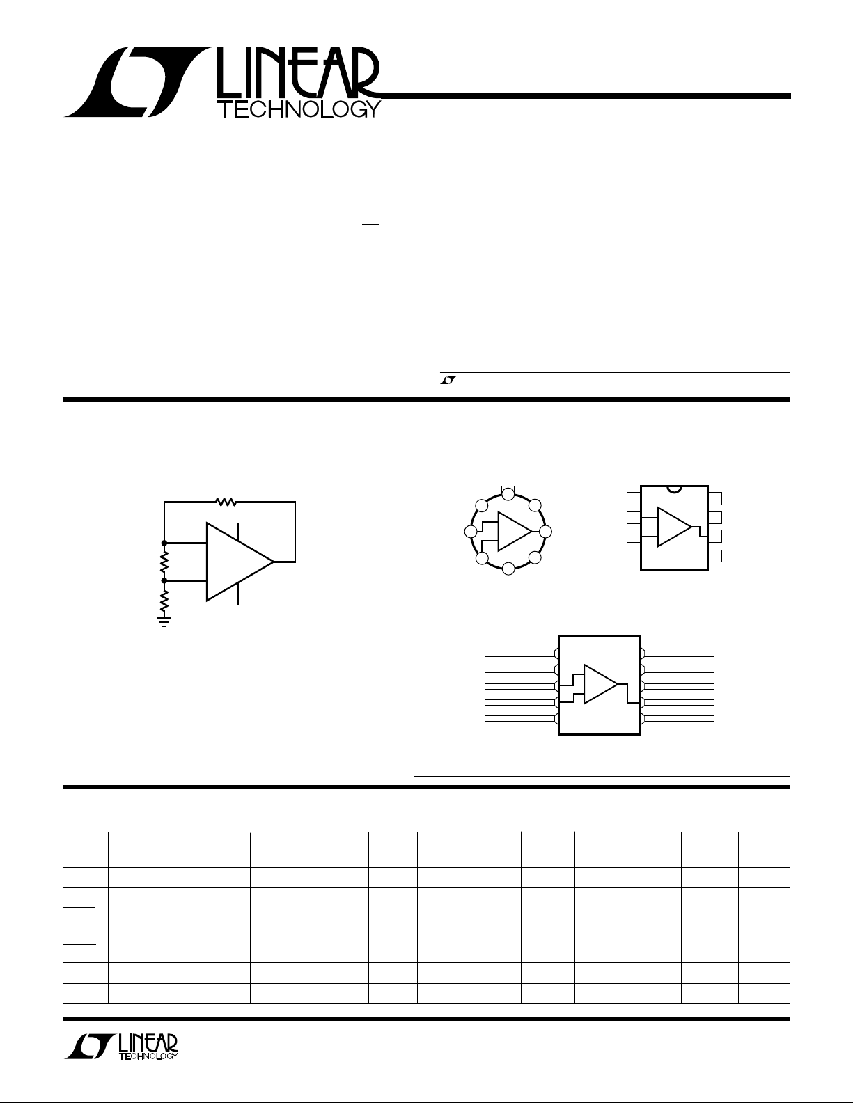
Precision Operational Amplifier
DUESCRIPTIO
The RH37C combines very low noise with excellent precision and high speed specifications. The low 1/f noise
corner frequency of 2.7Hz combined with 3.5nV√Hz 10Hz
noise and low offset voltage make the RH37C an excellent
choice for low frequency military instrumentation applications. The wafer lots are processed to LTC’s in-house
Class S flow to yield circuits usable in stringent military
applications.
For complete electrical specifications and performance
curves see the OP-27/OP-37 data sheet.
U U
BUR -I CIRCUIT
10k
20V
–
200Ω
10k
2
3
7
6
+
4
–20V
RH37C BI
A
W
O
LUTEXI T
S
A
WUW
ARB
U
G
I
S
Supply Voltage ..................................................... ±22V
Internal Power Dissipation................................ 500mW
Input Voltage ........................... Equal to Supply Voltage
Output Short-Circuit Duration ......................... Indefinite
Differential Input Current (Note 8) ..................... ±25mA
Operating Temperature Range ............. – 55°C to 125°C
Junction Temperature Range............... –55°C to 150°C
Storage Temperature Range ................ –65°C to 150°C
Lead Temperature (Soldering, 10 sec)................. 300°C
, LTC and LT are registered trademarks of Linear Technology Corporation.
TOP VIEW
VOS TRIM
V
OS
1
TRIM
2
–IN
3
+IN
V
H PACKAGE
8-LEAD TO-5 METAL CAN
8
–
+
4
–
(CASE)
+
V
7
6
OUT
5
NC
TOP VIEW
TABLE 1: ELECTRICAL CHARACTERISTICS
SYMBOL PARAMETER CONDITIONS NOTES MIN TYP MAX GROUP MIN TYP MAX GROUP UNITS
V
OS
∆V
∆Temp
∆V
∆Time Voltage Stability
I
OS
I
B
NC
1
V
TRIM
2
OS
–IN
3
4
+IN
–
5
V
–
+
W PACKAGE
10-LEAD CERPAC
(Preirradiation) (Note 9)
TA = 25°C SUB- SUB-
Input Offset Voltage 1 100 4 300 2, 3 µV
Average Offset Drift 4, 7 1.8 µV/°C
OS
Long-Term Input Offset 2, 4 2 µV/Month
OS
Input Offset Current 75 1 135 2, 3 nA
Input Bias Current ±80 1 ±150 2, 3 nA
–55°C ≤ TA ≤ 125°C
10
NC
V
TRIM
9
OS
+
V
8
7
OUT
6
NC
1
Page 2
RH37C
TABLE 1: ELECTRICAL CHARACTERISTICS
SYMBOL PARAMETER CONDITIONS NOTES MIN TYP MAX GROUP MIN TYP MAX GROUP UNITS
e
n
i
n
CMRR Common Mode VCM = ±11V 100 1 dB
PSRR Power Supply VS = ±4V to ±18V 94 1 dB
A
VOL
V
OUT
SR Slew Rate RL = 2k, A
GBW Gain-Bandwidth Product fO = 10kHz (A
Z
O
P
D
Input Noise Voltage 0.1Hz to 10Hz 4, 5 0.25 µV
Input Noise Voltage Density fO = 10Hz 3 8.0 nV/√Hz
= 30Hz 4 5.6 nV/√Hz
f
O
= 1000Hz 4 4.5 nV/√Hz
f
O
Input Noise Current Density fO = 1000Hz 4, 6 0.6 pV/√Hz
Input Resistance 2 GΩ
Common Mode
Input Voltage Range 4 ±11 ±10.2 V
Rejection Ratio VCM = ±10V 94 2, 3 dB
Rejection Ratio VS = ±4.5V to ±18V 86 2, 3 dB
Large-Signal Voltage Gain RL ≥ 2k, VO = ±10V 700 4 300 5, 6 V/mV
≥ 600Ω, VO = ±1V 4 200 V/mV
R
L
= ±4V
V
S
Maximum Output RL = 2k ±11.5 4 ±10.5 5, 6 V
Voltage Swing R
Open-Loop Output Resistance VO = 0, IO = 0 470 Ω
Power Dissipation 170 1 mW
= 600Ω±10.0 4 V
L
≥ 511 7 V/µs
VCL
≥ 5) 4 45 MHz
= 1MHz (A
f
O
VCL
≥ 5) 40 MHz
VCL
(Preirradiation) (Note 9)
TA = 25°C SUB- SUB-
–55°C ≤ TA ≤ 125°C
P-P
TABLE 1A: ELECTRICAL CHARACTERISTICS
10KRAD(Si)
SYMBOL PARAMETER CONDITIONS NOTES MIN MAX MIN MAX MIN MAX MIN MAX MIN MAX UNITS
V
OS
I
OS
I
B
CMRR Common Mode VCM = ±11V 100 100 97 94 90 dB
PSRR Power Supply VS = ±4V to ±18V 94 94 92 90 86 dB
A
VOL
V
OUT
SR Slew Rate RL ≥ 2k 1.7 1.7 1.7 1.5 1 V/µs
Z
O
P
D
Input Offset Voltage 1 100 130 180 280 400 µV
Input Offset Current 75 75 90 120 180 nA
Input Bias Current ±80 ±80 ±125 ±200 ±400 nA
Input Resistance 2 (Typ) 2 (Typ) 2 (Typ) 2 (Typ) 2 (Typ) GΩ
Common Mode
Input Voltage Range 4 ±11 ±11 ±11 ±11 ±11 V
Rejection Ratio
Rejection Ratio
Large-Signal Voltage Gain RL ≥ 2k, VO = ±10V 700 700 700 700 400 V/mV
Maximum Output RL ≥ 10k ±11.5 ±11.5 ±11.5 ±11.5 ±11.5 V
Voltage Swing RL ≥ 600Ω±10.0 ±10.0 ±10.0 ±10.0 ±10.0 V
Open-Loop Output Resistance VO = 0, IO = 0 70 (Typ) 70 (Typ) 70 (Typ) 70 (Typ) 70 (Typ) Ω
Power Dissipation 170 170 170 170 170 mW
(Postirradiation) (Note 10)
100KRAD(Si)50KRAD(Si)20KRAD(Si)
200KRAD(Si)
2
Page 3

TABLE 1A: ELECTRICAL CHARACTERISTICS
RH37C
Note 1: Input offset voltage measurements are performed by automatic
test equipment approximately 0.5 seconds after application of power.
Note 2: Long-term input offset voltage stability refers to the average trend
line of offset voltage vs time over the first 30 days of operation. Excluding
the initial hour of operation, changes in V
during the first 30 days are
OS
typically 2.5µV. Refer to the typical performance curves.
Note 3: Sample tested to an LTPD of 15 on every lot. Contact factory for
100% testing of 10Hz voltage density noise.
Note 4: Parameter is guaranteed by design, characterization, or correlation
to other tested parameters.
Note 5: See test circuit and frequency response curve for 0.1Hz to 10Hz
tester on OP-27/OP-37 data sheet.
TOTAL DOSE BIAS CIRCUIT
10k
15V
–
Note 6: See test circuit for current noise measurement on OP-27/OP-37
data sheet.
Note 7: The average input offset drift performance is within the specifications unnulled or when nulled with a pot having a range 8kΩ to 20kΩ.
Note 8: The RH37C’s inputs are protected by back-to-back diodes. Current
limiting resistors are not used in order to achieve low noise. If differential
input voltage exceeds ±0.7V, the input current should be limited to 25mA.
Note 9: V
Note 10: T
= ±15V, VCM = 0V unless otherwise noted.
S
= 25°C, VS = ±15V, VCM = 0V, unless otherwise noted.
A
10k
8V
+
–15V
WU
TYPICAL PERFOR A CE CHARACTERISTICS
Positive Slew Rate
25
VS = ±15V
= 2k
R
L
≥ 5
A
VCL
20
15
10
POSITIVE SLEW RATE (V/µs)
5
0
1
10
TOTAL DOSE KRAD (Si)
100 1000
RH37C G01
25
20
15
10
NEGATIVE SLEW RATE (V/µs)
0
Negative Slew Rate
V
= ±15V
S
= 2k
R
L
≥ 5
A
VCL
1
10
TOTAL DOSE KRAD (Si)
100 1000
RH37C G02
Information furnished by Linear Technology Corporation is believed to be accurate and reliable.
However, no responsibility is assumed for its use. Linear Technology Corporation makes no representation that the interconnection of its circuits as described herein will not infringe on existing patent rights.
3
Page 4

RH37C
TOTAL DOSE KRAD (Si)
1
110
120
140
100
RH37C G08
100
90
10 1000
80
70
130
POWER SUPPLY REJECTION RATIO (dB)
VS = ±4V TO ±18V
WU
TYPICAL PERFOR A CE CHARACTERISTICS
Input Offset Voltage Input Bias Current
150
VS = ±15V
= 0V
V
CM
100
50
0
–50
–100
INPUT OFFSET VOLTAGE (µV)
–150
–200
1
10 1000
TOTAL DOSE KRAD (Si)
100
RH37C G03
Common Mode Rejection Ratio Input Offset Current
170
VS = ±15V
= ±11V
V
CM
160
150
140
130
120
110
COMMON MODE REJECTION RATIO (dB)
100
1
10 1000
TOTAL DOSE KRAD (Si)
100
RH37C G06
Open-Loop Gain
170
160
150
140
130
120
OPEN-LOOP GAIN (dB)
110
100
1
75
VS = ±15V
V
CM
50
25
0
INPUT OFFSET CURRENT (nA)
–25
–50
1
10 1000
TOTAL DOSE KRAD (Si)
= 0V
10
TOTAL DOSE KRAD (Si)
VS = ±15V
R
L
V
OUT
100
100
= 2k
= ±10V
RH37C G04
RH37C G07
1000
350
VS = ±15V
V
CM
300
250
200
150
100
INPUT BIAS CURRENT (nA)
50
0
1
Power Supply Rejection Ratio
= 0V
10 1000
TOTAL DOSE KRAD (Si)
100
RH37C G05
TABLE 2: ELECTRICAL TEST REQUIRE E TS
MIL-STD-883 TEST REQUIREMENTS SUBGROUP
Final Electrical Test Requirements (Method 5004) 1*,2,3,4,5,6,7
Group A Test Requirements (Method 5005) 1,2,3,4,5,6,7
Group B and D for Class S, and 1
Group C and D for Class B
End Point Electrical Parameters (Method 5005)
* PDA applies to subgroup 1. See PDA Test Notes.
4
Linear Technology Corporation
1630 McCarthy Blvd., Milpitas, CA 95035-7417 ● (408) 432-1900
FAX: (408) 434-0507
●
TELEX: 499-3977 ● www.linear-tech.com
U
W
PDA Test Notes
The PDA is specified as 5% based on failures from group A, subgroup 1,
tests after cooldown as the final electrical test in accordance with method
5004 of MIL-STD-883 Class B. The verified failures of group A, subgroup
1, after burn-in divided by the total number of devices submitted for burnin in that lot shall be used to determine the percent for the lot.
Linear Technology Corporation reserves the right to test to tighter limits
than those given.
I.D. No. 66-10-0172 Rev. B 0398
rh37cb LT/HP 0398 100 REV B • PRINTED IN USA
LINEAR TECHNOLOGY CORPORATION 1993
 Loading...