

Page 1

RH1078M
WU
U
PACKAGE
/
O
RDER I FOR ATIO
TOP VIEW
OUT BOUT A
V
+
–IN B–IN A
+IN B+IN A
V
–
8
7
6
5
3
2
1
4
H PACKAGE
8-LEAD TO-5 METAL CAN
Micropower, Dual, Single Supply
Precision Op Amp
DUESCRIPTIO
The RH1078M is a micropower dual op amp in the
standard 8-pin configuration. This device is optimized for
single supply operation at 5V. Specifications for ±15V are
also provided.
The wafer lots are processed to LTC’s in-house Class S
flow to yield circuits usable in stringent military applications.
U
U
BUR -I CIRCUIT
(Each Amplifier)
50k
20V
–
W
O
A
Supply Voltage ..................................................... ±22V
Differential Input Voltage ...................................... ±30V
Input Voltage ...............Equal to Positive Supply Voltage
...............................0.5V Below Negative Supply Voltage
Output Short-Circuit Duration ......................... Indefinite
Operating Temperature Range ............. – 55°C to 125°C
Storage Temperature Range ................ –55°C to 150°C
Lead Temperature (Soldering, 10 sec)................. 300°C
LUTEXI T
S
A
WUW
ARB
U
G
I
S
100Ω
+
50k
–20V
TOTAL DOSE BIAS CIRCUIT
10k
15V
–
10k
8V
Note: For ordering information contact LTC.
+
–15V
1
Page 2
RH1078M
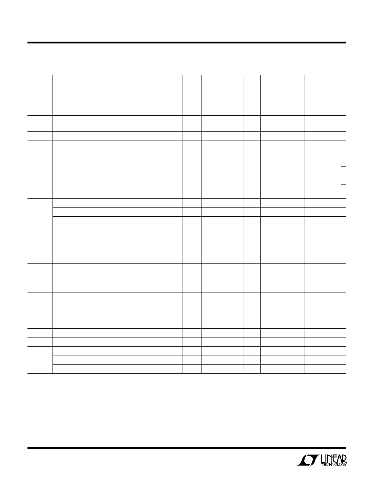
TABLE 1: ELECTRICAL CHARACTERISTICS
VS = 5V, VCM = 0.1V, V
SYMBOL PARAMETER CONDITIONS NOTES MIN TYP MAX GROUP MIN TYP MAX GROUP UNITS
V
OS
∆V
OS
∆Temp Offset Voltage
∆V
OS
∆Time
I
OS
I
B
e
n
i
n
R
IN
CMRR Common-Mode VCM = 0V to 3.5V 94 1 dB
PSRR Power Supply VS = 2.3V to 12V 100 1 dB
A
VOL
V
OUT
SR Slew Rate AV = 1, VS = ±2.5V 0.04 4 V/µs
GBW Gain-Bandwidth Product fO ≤ 20kHz 200 kHz
I
S
Input Offset Voltage 120 4 370 2, 3 µV
Average Tempco of 0.5 µV/°C
Long Term VOS Stability 0.5 µV/Month
Input Offset Current 0.8 1 1.5 2, 3 nA
Input Bias Current 15 1 18 2, 3 nA
Input Noise Voltage 0.1Hz to 10Hz 1 0.5 µVP-P
Input Noise Voltage Density fO = 10Hz 1 25 nV/√Hz
Input Noise Current 0.1Hz to 10Hz 1 2.6 pAP-P
Input Noise Current Density fO = 10Hz 1 0.07 pA/√Hz
Input Resistance Differential 2 600 MΩ
Common Mode 2 5 GΩ
Input Voltage Range 2 3.5 1 3.20 2, 3 V
Rejection Ratio VCM = 0.05V to 3.2V 88 2, 3 dB
Rejection Ratio V
Large-Signal Voltage Gain VO = 0.03V to 4V, No Load 150 1 V/mV
Output Voltage Swing Output Low, No Load 6 4 8 5, 6 mV
Supply Current per Amplifier 75 1 95 2, 3 µA
Channel Separation ∆VIN = 3V, RL = 10k 130 dB
Minimum Supply Voltage 3 2.3 V
= 1.4V unless otherwise specified.
OUT
= 1kHz 1 24 nV/√Hz
f
O
= 1kHz 1 0.025 pA/√Hz
f
O
= 3.1V to 12V 94 2, 3 dB
S
= 0.03V to 3.5V, RL = 50k 120 1 V/mV
V
O
= 0.05V to 4V, No Load 80 2, 3 V/mV
V
O
= 0.05V to 3.5V, RL = 50k 60 2, 3 V/mV
V
O
Output Low, 2k to GND 2 4 mV
Output Low, I
Output High, No Load 4.2 4 3.9 5, 6 V
Output High, 2k to GND 3.5 4 3.0 5, 6 V
= 100µA 130 4 170 5, 6 mV
SINK
2 0 1 0.05 2, 3 V
(Preirradiation)
TA = 25°C SUB- SUB-
–55°C ≤ TA ≤ 125°C
2
Page 3
RH1078M
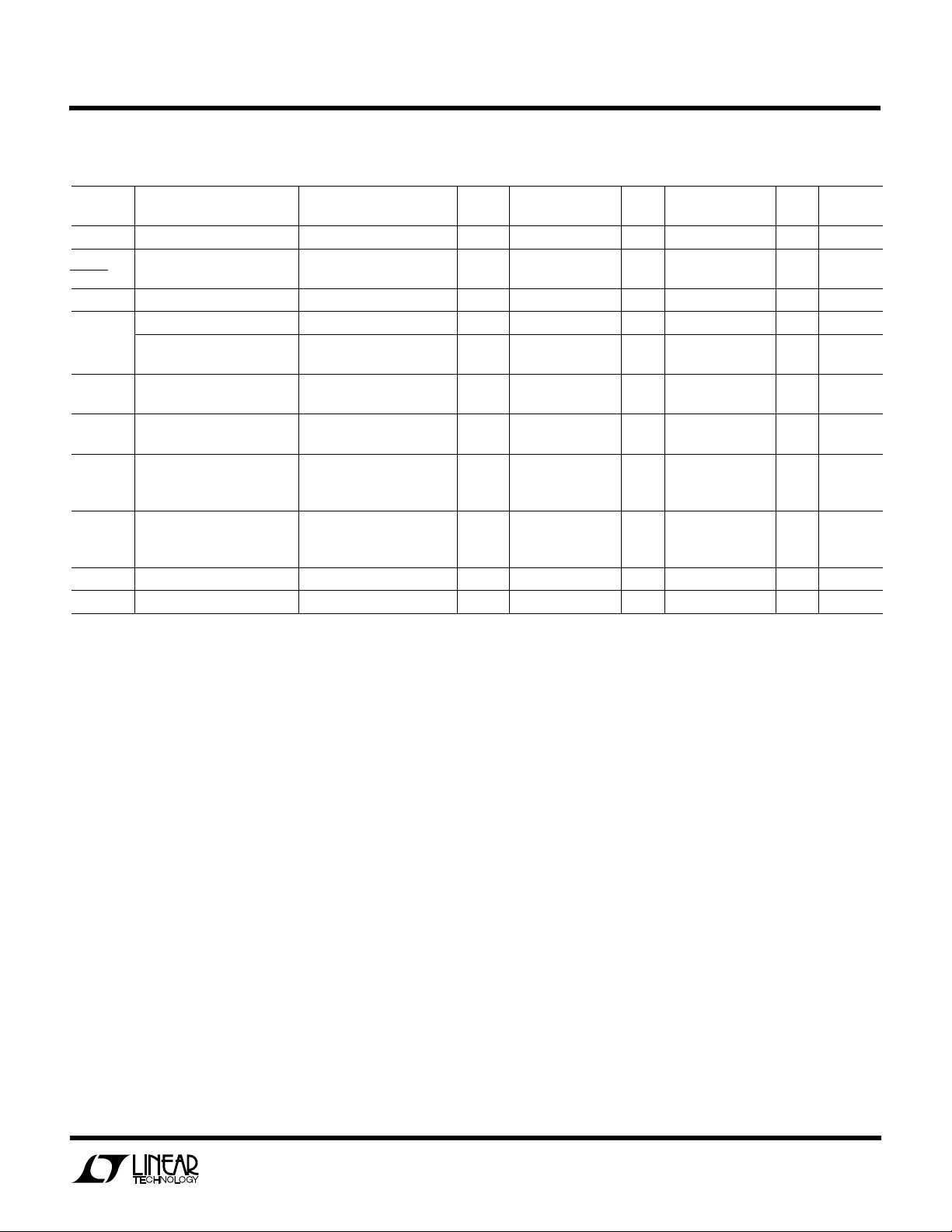
TABLE 1: ELECTRICAL CHARACTERISTICS
(Preirradiation)
VS = ±15V unless otherwise specified.
TA = 25°C SUB- SUB-
SYMBOL PARAMETER CONDITIONS NOTES MIN TYP MAX GROUP MIN TYP MAX GROUP UNITS
V
OS
∆V
OS
∆Temp Offset Voltage
I
OS
I
B
CMRR Common-Mode VCM = 13.5V, –15V 97 1 dB
PSRR Power Supply VS = 5V, 0V to ±18V 100 1 94 2, 3 dB
A
VOL
V
OUT
SR Slew Rate 0.06 4 V/µs
I
S
Input Offset Voltage 350 4 600 2, 3 µV
Average Tempco of 0.6 µV/°C
Input Offset Current 0.8 1 1.5 2, 3 nA
Input Bias Current 15 18 2, 3 nA
Input Voltage Range 13.5 1 V
–15.0 1 V
Rejection Ratio V
Rejection Ratio
Large-Signal Voltage Gain VO = ±10V, RL = 50k 1000 1 V/mV
Output Voltage Swing RL = 50k ±13 4 V
Supply Current Per Amplifier 100 1 125 2, 3 µA
= 13V, –14.9V 90 2, 3 dB
CM
= ±10V, RL = 2k 300 1 V/mV
V
O
VO = ±10V, RL = 5k 150 2, 3 V/mV
= 2k ±11 4 V
R
L
= 5k ±11 5, 6 V
R
L
–55°C ≤ TA ≤ 125°C
Note 1: All noise parameters are for VS = ±2.5V, VO = 0V.
Note 2: This parameter is guaranteed by design, characterization or
correlation to other tested parameters.
Note 3: Power supply rejection ratio is measured at the minimum supply
voltage. The op amps actually work at 1.8V supply but with a typical offset
skew of –300µV.
3
Page 4

RH1078M
TABLE 1A: ELECTRICAL CHARACTERISTICS (Postirradiation)
VS = 5V, 0V, VCM = 0.1V, V0 = 1.4V, TA = 25°C unless otherwise noted.
25KRAD(Si)10KRAD(Si)
SYMBOL PARAMETER CONDITIONS MIN MAX MIN MAX MIN MAX MIN MAX MIN MAX UNITS
V
OS
I
OS
I
B
CMRR Common-Mode VCM = 0V to 3.5V 91 89 87 85 dB
PSRR Power Supply VS = 2.3V to 12V 100 100 98 88 dB
A
VOL
V
OUT
S
R
I
S
Input Offset Voltage 120 175 250 500 µV
Input Offset Current 2 8 13 18 nA
Input Bias Current 20 40 80 100 nA
Input Voltage Range 3.5 3.5 3.5 3.5 V
Rejection Ratio
Rejection Ratio
Large-Signal VO = 0.03V to 4V, No Load 150 150 100 50 V/mV
Voltage Gain V
Output Voltage Output Low, No Load 6 9 13 20 mV
Swing Output Low, 2k to GND 2 2 2 2 mV
Slew Rate AV = 1, VS = ±2.5V 0.04 0.03 0.02 0.01 V/µs
Supply Current per Amplifier 75 75 75 75 µA
= 0.03V to 3.5V, RL = 50k 120 50 20 10 V/mV
O
Output Low, I
Output High, No Load 4.2 4.2 4.2 4.2 V
Output High, 2k to GND 3.5 3.5 3.5 3.5 V
= 100µA 130 140 150 160 mV
SINK
75KRAD(Si)50KRAD(Si)
100KRAD(Si)
4
Page 5

RH1078M
TABLE 1A: ELECTRICAL CHARACTERISTICS
(Postirradiation)
VS = ±15V unless otherwise noted.
25KRAD(Si)10KRAD(Si)
SYMBOL PARAMETER CONDITIONS MIN MAX MIN MAX MIN MAX MIN MAX MIN MAX UNITS
V
OS
I
OS
I
B
CMRR Common-Mode VCM = 13.5V, –15V 94 92 90 88 86 dB
PSRR Power Supply VS = 5V, 0V to ±18V 100 100 98 88 78 dB
A
VOL
V
OUT
SR Slew Rate 0.05 0.04 0.03 0.02 0.01 V/µs
I
S
Input Offset Voltage 350 500 650 800 1000 µV
Input Offset Current 2 8 13 18 23 nA
Input Bias Current 20 40 80 100 120 nA
Input Voltage Range 13.5 13.5 13.5 13.5 13.5 V
–15.0 –15.0 –15.0 –15.0 –15.0 V
Rejection Ratio
Rejection Ratio
Large-Signal VO = 10V, RL = 50k 1000 700 400 150 50 V/mV
Voltage Gain V
Output Voltage RL = 50k ±13 ±13 ±13 ±13 ±13 V
Swing R
Supply Current per Amplifier 100 100 100 100 100 µA
= 10V, RL = 2k 300 200 120 45 15 V/mV
O
= 2k ±11 ±11 ±11 ±11 ±10 V
L
75KRAD(Si)50KRAD(Si)
100KRAD(Si)
5
Page 6

RH1078M
TOTAL DOSE-KRADs (Si)
1
110
COMMON-MODE REJECTION RATIO (dB)
120
130
10 100 1000
1078M • G4
100
90
U
W
TABLE 2: ELECTRICAL TEST REQUIRE E TS
MIL-STD-883 TEST REQUIREMENTS SUBGROUP
Final Electrical Test Requirements (Method 5004) 1*,2,3,4,5,6
Group A Test Requirements (Method 5005) 1,2,3,4,5,6
Group C and D End Point Electrical Parameters 1,2,3
(Method 5005)
* PDA Applies to subgroup 1. See PDA Test Notes.
U
TYPICAL APPLICATIONS
Input Offset Voltage
1000
750
500
250
0
–250
–500
INPUT OFFSET VOLTAGE (µV)
–750
PDA Test Notes
The PDA is specified as 5% based on failures from group A, subgroup 1, tests
after cooldown as the final electrical test in accordance with method 5004 of
MIL-STD-883 Class B. The verified failures of group A, subgroup 1, after burnin divided by the total number of devices submitted for burn-in in that lot shall
be used to determine the percent for the lot.
Linear Technology Corporation reserves the right to test to tighter limits than
those given.
Input Offset Current
20
15
10
5
0
–5
–10
INPUT OFFSET CURRENT (nA)
–15
–1000
1
10 100 1000
TOTAL DOSE-KRADs (Si)
Input Bias Current
0
–20
–40
–60
–80
–100
–120
INPUT BIAS CURRENT (nA)
–140
–160
1
10 100 1000
TOTAL DOSE-KRADs (Si)
1078M • G1
1078M • G3
–20
1
10 100 1000
TOTAL DOSE-KRADs (Si)
Common-Mode Rejection Ratio
1078M • G2
6
Page 7

TOTAL DOSE-KRADs (Si)
1
110
LARGE-SIGNAL VOLTAGE GAIN (dB)
130
150
10 100 1000
1078M • G6
90
100
120
140
80
70
VS = ±15V
V
O
= ±10V
R
L
= 2k
V
S
= 5V, 0V
V
O
= 0.03V TO 3.5V
R
L
= 50k
U
TYPICAL APPLICATIONS
RH1078M
Power Supply Rejection Ratio
140
130
120
110
100
90
80
70
POWER SUPPLY REJECTION RATIO (dB)
60
1
10 100 1000
TOTAL DOSE-KRADs (Si)
Slew Rate
0.16
0.14
SLEW RATE (V/µs)
0.12
0.10
0.08
0.06
0.04
0.02
VS = 5V, 0V
0
1
10 100 1000
TOTAL DOSE-KRADs (Si)
VS = ±15V
1078M • G5
1078M • G7
Large-Signal Voltage Gain
Gain-Bandwidth Product
400
VS = ±15V
350
300
250
200
150
100
GAIN-BANDWIDTH PRODUCT (kHz)
50
0
1
10 100 1000
TOTAL DOSE-KRADs (Si)
1078M • G8
160
140
120
100
10Hz NOISE DENSITY (nV/√Hz)
10Hz Noise Density
VS = ±15V
80
60
40
20
0
1
10 100 1000
TOTAL DOSE-KRADs (Si)
Positive Output Voltage Swing
16
VS = ±15V
14
12
10
8
6
4
2
POSITIVE OUTPUT VOLTAGE SWING (V)
0
1
1078M • G9
Information furnished by Linear Technology Corporation is believed to be accurate and reliable.
However, no responsibility is assumed for its use. Linear Technology Corporation makes no representation that the interconnection of its circuits as described herein will not infringe on existing patent rights.
10 100 1000
TOTAL DOSE-KRADs (Si)
R
= 50k
L
RL = 2k
1078M • G10
7
Page 8

RH1078M
TOTAL DOSE-KRADs (Si)
1
16
OUTPUT VOLTAGE SWING (mV)
20
26
10 100 1000
1078M • G12
8
12
18
24
4
0
VS = 5V, 0V
U
TYPICAL APPLICATIONS
Negative Output Voltage Swing
0
VS = ±15V
–2
–4
–6
–8
–10
–12
–14
NEGATIVE OUTPUT VOLTAGE SWING (V)
–16
1
10 100 1000
TOTAL DOSE-KRADs (Si)
RL = 2k
= 50k
R
L
1078M • G11
Output Voltage Swing Low,
No Load
8
Linear Technology Corporation
1630 McCarthy Blvd., Milpitas, CA 95035-7417 ● (408) 432-1900
FAX: (408) 434-0507
Output Voltage Swing Low,
2k to GND
1.6
VS = 5V, 0V
1.4
1.2
1.0
0.8
0.6
0.4
OUTPUT VOLTAGE SWING (mV)
0.2
0
1
10 100 1000
TOTAL DOSE-KRADs (Si)
Output Voltage Swing High
4.6
VS = 5V, 0V
4.4
4.2
4.0
3.8
3.6
3.4
OUTPUT VOLTAGE SWING (V)
3.2
3.0
1
10 100 1000
TOTAL DOSE-KRADs (Si)
●
TELEX: 499-3977 ● www.linear-tech.com
1078M • G13
NO LOAD
2k TO GND
1078M • G15
Output Voltage Swing Low,
I
= 100mA
SINK
160
VS = 5V, 0V
140
120
100
80
60
40
OUTPUT VOLTAGE SWING (mV)
20
0
1
10 100 1000
TOTAL DOSE-KRADs (Si)
Supply Current
80
70
60
50
40
30
20
10
SUPPLY CURRENT PER AMPLIFIER (µA)
0
VS = 5V, 0V
1
10 100 1000
TOTAL DOSE-KRADs (Si)
rh1078me LT/TP 0798 500 REV E • PRINTED IN USA
LINEAR TECHNOLOGY CORPORATION 1994
1078M • G14
VS = 15V
1078M • G16
I.D. No. 66-10-0100 Rev. E 0798
 Loading...