

Page 1
Semiconductor
/
j
/
/
/
/
/
/
/
RFM3N45, RFM3N50, RFP3N45, RFP3N50
Data Sheet October 1998 File Number 1384.2
[ /Title
()
Subect ()
Autho
r ()
Keywords
()
Creator ()
DOCI
NFO
pdfmark
[
PageMode
UseOutlines
DOCVIEW
pdfmark
3A, 450V and 500V, 3 Ohm, N-Channel
Power MOSFETs
These are N-Channel enhancement mode silicon gate
power field effect transistors designed for applications such
as switching regulators, switching converters, motor drivers,
relay drivers, and drivers for high power bipolar switching
transistors requiring high speed and low gate drive power.
These types can be operated directly from integrated
circuits.
Formerly developmental type TA17405.
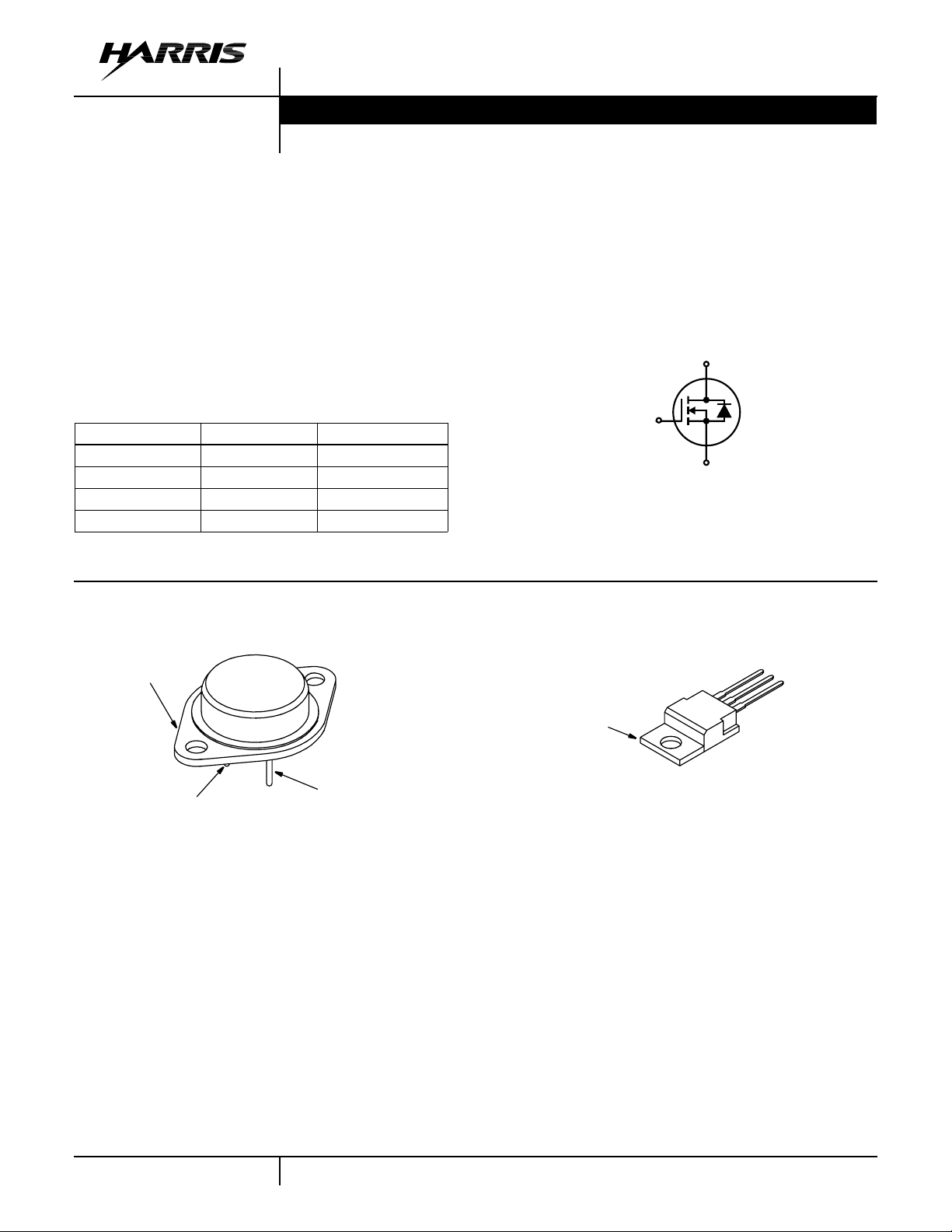
Ordering Information
PART NUMBER PACKAGE BRAND
RFM3N45 TO-204AA RFM3N45
RFM3N50 TO-204AA RFM3N50
RFP3N45 TO-220AB RFP3N45
RFP3N50 TO-220AB RFP3N50
NOTE: When ordering, use the entire part number.
Packaging
JEDEC TO-204AA JEDEC TO-220AB
DRAIN
(FLANGE)
GATE (PIN 1)
SOURCE (PIN 2)
Features
• 3A, 450V and 500V
•r
• Related Literature
- TB334 “Guidelines for Soldering Surface Mount
= 3Ω
DS(ON)
Components to PC Boards”
Symbol
D
G
S
SOURCE
DRAIN
DRAIN (FLANGE)
GATE
1
CAUTION: These devices are sensitive to electrostatic discharge; follow proper IC Handling Procedures.
1-800-4-HARRIS
| Copyright © Harris Corporation 1998
Page 2

RFM3N45, RFM3N50, RFP3N45, RFP3N50
Absolute Maximum Ratings T
= 25oC, Unless Otherwise Specified
C
RFM3N45 RFM3N50 RFP3N45 RFP3N50 UNITS
Drain to Source Breakdown Voltage (Note 1) . . . . . . . . . V
Drain to Gate Voltage (RGS = 20kΩ) (Note 1) . . . . . . . . V
DGR
Continuous Drain Current . . . . . . . . . . . . . . . . . . . . . . . . . . I
Pulsed Drain Current (Note 3) . . . . . . . . . . . . . . . . . . . . . .I
Gate to Source Voltage . . . . . . . . . . . . . . . . . . . . . . . . . . V
Maximum Power Dissipation . . . . . . . . . . . . . . . . . . . . . . . P
DS
D
DM
GS
D
450 500 450 500 V
450 500 450 500 V
3333A
5555A
±20 ±20 ±20 ±20 V
75 75 60 60 W
Linear Derating Factor. . . . . . . . . . . . . . . . . . . . . . . . . . . . . . . 0.6 0.6 0.48 0.48 W/oC
Operating and Storage Temperature . . . . . . . . . . . . TJ, T
STG
-55 to 150 -55 to 150 -55 to 150 -55 to 150
Maximum Temperature for Soldering
Leads at 0.063in (1.6mm) from Case for 10s. . . . . . . . . .T
Package Body for 10s, See Techbrief 334 . . . . . . . . . .T
CAUTION: Stresses above those listed in “Absolute Maximum Ratings” may cause permanent damage to the device. This is a stress only rating and operationofthe
device at these or any other conditions above those indicated in the operational sections of this specification is not implied.
L
pkg
300
260
300
260
300
260
300
260
o
C
o
C
o
C
NOTE:
1. TJ= 25oC to 125oC.
Electrical Specifications T
= 25oC, Unless Otherwise Specified
C
PARAMETER SYMBOL TEST CONDITIONS MIN TYP MAX UNITS
Drain to Source Breakdown Voltage BV
DSSID
= 250µA, VGS = 0V
RFM3N45, RFP3N45 450 - - V
RFM3N50, RFP3N50 500 - - V
Gate Threshold Voltage V
GS(TH)VGS
Zero Gate Voltage Drain Current I
Gate to Source Leakage Current I
Drain to Source On Resistance (Note 2) r
Drain to Source On Voltage (Note 2) V
Turn-On Delay Time t
DS(ON)ID
DS(ON)ID
d(ON)VDD
Rise Time t
Turn-Off Delay Time t
d(OFF)
Fall Time t
Input Capacitance C
Output Capacitance C
Reverse Transfer Capacitance C
Thermal Resistance, Junction to Case R
DSS
GSS
r
f
ISS
OSS
RSS
θJC
= VDS, ID = 250µA, (Figure 7) 2.0 - 4.0 V
VDS = Rated BV
VDS = 0.8 x Rated BV
, VGS = 0V - - 1 µA
DSS
, VGS = 0V, TC = 125oC- - 25 µA
DSS
VGS = ±20V, VDS = 0V - - ±100 nA
= 3A, VGS = 10V, (Figures 5, 6) - - 3 Ω
= 3A, VGS = 10V - - 9.0 V
= 250V, I
RL = 165Ω
(Figures 10, 11, 12)
≈ 1.5A, R
D
= 50Ω, VGS = 10V
G
-3045ns
-4060ns
- 90 135 ns
-5075ns
VDS = 25V, VGS = 0V, f = 1MHz - - 750 pF
- - 150 pF
- - 100 pF
RFM3N45, RFM3N50 - - 1.67oC/W
RFP3N45, RFP3N50 - - 2.083oC/W
Source to Drain Diode Specifications
PARAMETER SYMBOL TEST CONDITIONS MIN TYP MAX UNITS
Source to Drain Diode Voltage (Note 2) V
Reverse Recovery Time t
NOTES:
2. Pulse test: pulse width ≤ 300µs, duty cycle ≤ 2%.
3. Repetitive rating: pulse width limited by maximum junction temperature.
2
ISD = 1.5A - - 1.4 V
SD
ISD = 4A, dISD/dt = 100A/µs - 800 - ns
rr
Page 3
RFM3N45, RFM3N50, RFP3N45, RFP3N50
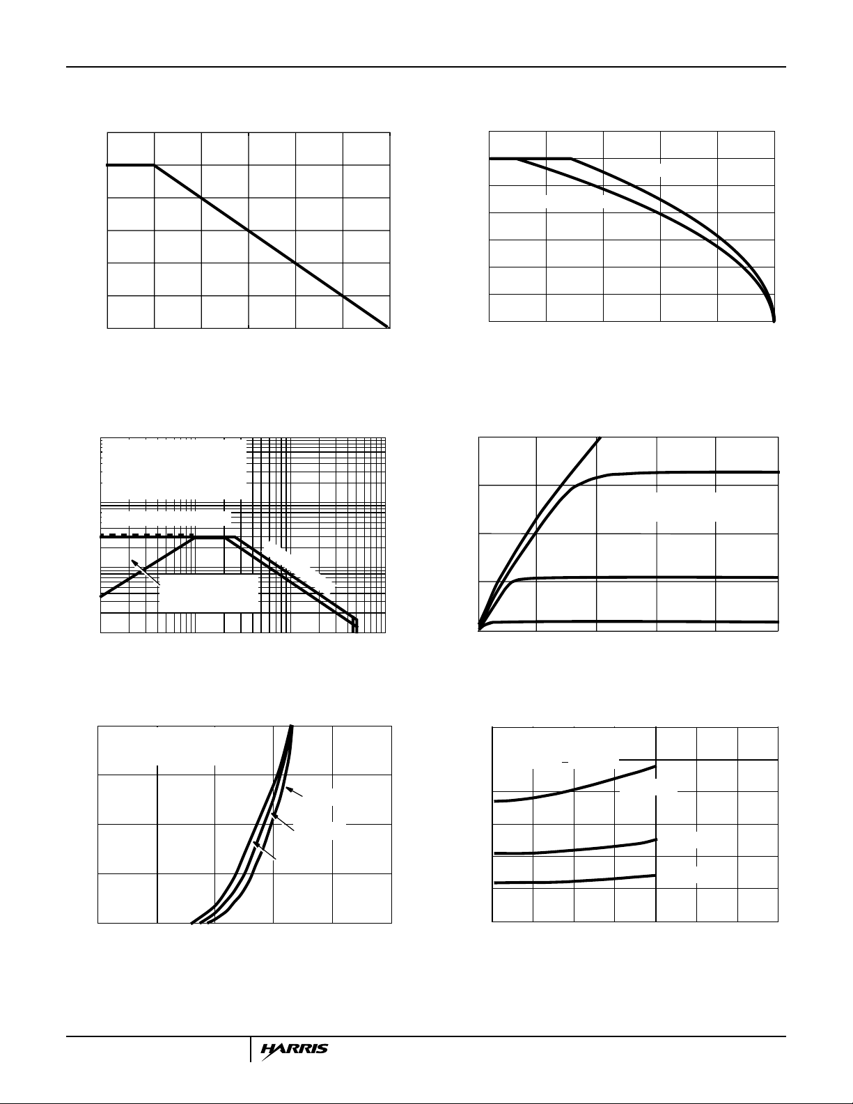
Typical Performance Curves
1.2
1.0
0.8
0.6
0.4
0.2
POWER DISSIPATION MULTIPLIER
0
0 25 50 75 100 150
TC, CASE TEMPERATURE (oC)
Unless Otherwise Specified
125
FIGURE 1. NORMALIZED POWER DISSIPATIONvsCASE
TEMPERATURE
100
TC = 25oC
(CURVES MUST BE DERATED
LINEARLY WITH INCREASE
IN TEMPERATURE)
10
ID (MAX.) CONTINUOUS
DC OPERATION
1
, DRAIN CURRENT (A)
D
I
0.1
1 10 100 1000
OPERATION IN THIS
AREA MAY BE
LIMITED BY r
V
DRAIN TO SOURCE VOLTAGE (V)
DS,
DS(ON)
3.5
3
2.5
RFP3N45, RFP3N50
2
1.5
1
, DRAIN CURRENT (A)
D
I
0.5
0
25 50 75 100 125 150
, CASE TEMPERATURE (oC)
T
C
RFM3N45, RFM3N50
FIGURE 2. MAXIMUM CONTINUOUS DRAIN CURRENT vs
CASE TEMPERATURE
4
3
2
, DRAIN CURRENT (A)
1
D
I
0
0 5 10 15 20 25
V
DS
V
= 10V
GS
, DRAIN TO SOURCE VOLTAGE (V)
V
= 6V
GS
PULSE DURATION = 80µs
DUTY CYCLE ≤ 2%
VGS = 5V
V
= 4V
GS
FIGURE 3. FORWARD BIAS SAFE OPERATING AREA FIGURE 4. SATURATION CHARACTERISTICS
4
VDS = 10V
PULSE DURATION = 80µs
DUTY CYCLE ≤ 2%
3
TC = -40oC
2
1
, DRAIN TO SOURCE CURRENT (A)
DS(ON)
I
0
0246810
V
, GATE TO SOURCE VOLTAGE (V)
GS
TC = 25oC
TC = 125oC
6
VGS = 10V
PULSE DURATION = 80µs
DUTY CYCLE
5
4
3
, DRAIN TO SOURCE
2
ON RESISTANCE (Ω)
DS(ON)
1
r
0
01234567
< 2%
TC = 125oC
I
, DRAIN CURRENT (A)
D
TC = 25oC
TC = -40oC
FIGURE 5. TRANSFER CHARACTERISTICS FIGURE 6. DRAIN TO SOURCE ON RESISTANCE vs GATE
VOLTAGE AND DRAIN CURRENT
3
Page 4

RFM3N45, RFM3N50, RFP3N45, RFP3N50
Typical Performance Curves
2
ID = 3A, VGS =10V
PULSE DURATION = 80µs
1.5
1
ON RESISTANCE
0.5
NORMALIZED DRAIN TO SOURCE
0
-50 0 50 100 150 200
, JUNCTION TEMPERATURE (oC)
T
J
Unless Otherwise Specified (Continued)
FIGURE 7. NORMALIZED DRAIN TO SOURCEON
RESISTANCE vs JUNCTION TEMPERATURE
800
700
600
500
400
300
C, CAPACITANCE (pF)
200
100
0
0 10203040 5060708090100
VDS, DRAIN TO SOURCE VOLTAGE (V)
VGS = 0V, f = 1MHz
C
ISS
C
RSS
C
OSS
C
ISS
C
OSS
C
RSS
= CGS + C
= C
≈ CDS + C
GD
GD
GD
1.4
VDS = 10V
1.3
= 250µA
I
D
1.2
1.1
1.0
0.9
NORMALIZED GATE
0.8
THRESHOLD VOLTAGE
0.7
0.6
-50
0 50 100 150 200
, JUNCTION TEMPERATURE(oC)
T
J
FIGURE 8. NORMALIZED GATETHRESHOLDVOLTAGE vs
JUNCTION TEMPERATURE
500
375
250
125
, DRAIN TO SOURCE VOLTAGE (V)
DS
V
VDD= BV
0
20
DSS
SOURCE
VOLTAGE
R
I
G(REF)
VGS = 10V
0.75BV
0.50BV
0.25BV
DRAIN SOURCE VOLTAGE
I
G(REF)
I
G(ACT)
t, TIME (µs)
GATE
= 167Ω
L
= 0.45mA
DSS
DSS
DSS
VDD= BV
I
80
I
DSS
G(REF)
G(ACT)
10
8
6
4
2
, GATE TO SOURCE VOLTAGE (V)
GS
V
0
FIGURE 9. CAPACITANCE vs DRAIN TO SOURCE VOLTAGE
4
NOTE: Refer to Harris Application Notes AN7254 and AN7260.
FIGURE 10. NORMALIZED SWITCHING WAVEFORMS FOR
CONSTANT GATE CURRENT
Page 5

RFM3N45, RFM3N50, RFP3N45, RFP3N50
Test Circuits and Waveforms
R
G
V
GS
FIGURE 11. SWITCHING TIME TEST CIRCUIT
CURRENT
REGULATOR
12V
BATTERY
0.2µF
50kΩ
0.3µF
G
t
ON
t
d(ON)
t
R
L
+
V
DD
-
DUT
V
DS
0
V
GS
0
90%
10%
r
10%
50%
PULSE WIDTH
t
d(OFF)
90%
t
OFF
50%
t
f
90%
10%
FIGURE 12. RESISTIVE SWITCHING WAVEFORMS
V
DS
(ISOLATED
SUPPLY)
SAME TYPE
AS DUT
D
DUT
V
DD
Q
g(TOT)
Q
gd
Q
gs
V
DS
0
V
GS
I
0
G(REF)
IG CURRENT
SAMPLING
RESISTOR RESISTOR
FIGURE 13. GATE CHARGE TEST CIRCUIT
S
CURRENT
I
D
SAMPLING
V
DS
0
I
G(REF)
FIGURE 14. GATE CHARGE WAVEFORMS
5
Page 6

Semiconductor
/
j
/
/
/
/
/
/
/
RFM3N45, RFM3N50, RFP3N45, RFP3N50
Data Sheet October 1998 File Number 1384.2
[ /Title
()
Subect ()
Autho
r ()
Keywords
()
Creator ()
DOCI
NFO
pdfmark
[
PageMode
UseOutlines
DOCVIEW
pdfmark
3A, 450V and 500V, 3 Ohm, N-Channel
Power MOSFETs
These are N-Channel enhancement mode silicon gate
power field effect transistors designed for applications such
as switching regulators, switching converters, motor drivers,
relay drivers, and drivers for high power bipolar switching
transistors requiring high speed and low gate drive power.
These types can be operated directly from integrated
circuits.
Formerly developmental type TA17405.
Ordering Information
PART NUMBER PACKAGE BRAND
RFM3N45 TO-204AA RFM3N45
RFM3N50 TO-204AA RFM3N50
RFP3N45 TO-220AB RFP3N45
RFP3N50 TO-220AB RFP3N50
NOTE: When ordering, use the entire part number.
Packaging
JEDEC TO-204AA JEDEC TO-220AB
DRAIN
(FLANGE)
GATE (PIN 1)
SOURCE (PIN 2)
Features
• 3A, 450V and 500V
•r
• Related Literature
- TB334 “Guidelines for Soldering Surface Mount
= 3Ω
DS(ON)
Components to PC Boards”
Symbol
D
G
S
SOURCE
DRAIN
DRAIN (FLANGE)
GATE
1
CAUTION: These devices are sensitive to electrostatic discharge; follow proper IC Handling Procedures.
1-800-4-HARRIS
| Copyright © Harris Corporation 1998
Page 7

RFM3N45, RFM3N50, RFP3N45, RFP3N50
Absolute Maximum Ratings T
= 25oC, Unless Otherwise Specified
C
RFM3N45 RFM3N50 RFP3N45 RFP3N50 UNITS
Drain to Source Breakdown Voltage (Note 1) . . . . . . . . . V
Drain to Gate Voltage (RGS = 20kΩ) (Note 1) . . . . . . . . V
DGR
Continuous Drain Current . . . . . . . . . . . . . . . . . . . . . . . . . . I
Pulsed Drain Current (Note 3) . . . . . . . . . . . . . . . . . . . . . .I
Gate to Source Voltage . . . . . . . . . . . . . . . . . . . . . . . . . . V
Maximum Power Dissipation . . . . . . . . . . . . . . . . . . . . . . . P
DS
D
DM
GS
D
450 500 450 500 V
450 500 450 500 V
3333A
5555A
±20 ±20 ±20 ±20 V
75 75 60 60 W
Linear Derating Factor. . . . . . . . . . . . . . . . . . . . . . . . . . . . . . . 0.6 0.6 0.48 0.48 W/oC
Operating and Storage Temperature . . . . . . . . . . . . TJ, T
STG
-55 to 150 -55 to 150 -55 to 150 -55 to 150
Maximum Temperature for Soldering
Leads at 0.063in (1.6mm) from Case for 10s. . . . . . . . . .T
Package Body for 10s, See Techbrief 334 . . . . . . . . . .T
CAUTION: Stresses above those listed in “Absolute Maximum Ratings” may cause permanent damage to the device. This is a stress only rating and operationofthe
device at these or any other conditions above those indicated in the operational sections of this specification is not implied.
L
pkg
300
260
300
260
300
260
300
260
o
C
o
C
o
C
NOTE:
1. TJ= 25oC to 125oC.
Electrical Specifications T
= 25oC, Unless Otherwise Specified
C
PARAMETER SYMBOL TEST CONDITIONS MIN TYP MAX UNITS
Drain to Source Breakdown Voltage BV
DSSID
= 250µA, VGS = 0V
RFM3N45, RFP3N45 450 - - V
RFM3N50, RFP3N50 500 - - V
Gate Threshold Voltage V
GS(TH)VGS
Zero Gate Voltage Drain Current I
Gate to Source Leakage Current I
Drain to Source On Resistance (Note 2) r
Drain to Source On Voltage (Note 2) V
Turn-On Delay Time t
DS(ON)ID
DS(ON)ID
d(ON)VDD
Rise Time t
Turn-Off Delay Time t
d(OFF)
Fall Time t
Input Capacitance C
Output Capacitance C
Reverse Transfer Capacitance C
Thermal Resistance, Junction to Case R
DSS
GSS
r
f
ISS
OSS
RSS
θJC
= VDS, ID = 250µA, (Figure 7) 2.0 - 4.0 V
VDS = Rated BV
VDS = 0.8 x Rated BV
, VGS = 0V - - 1 µA
DSS
, VGS = 0V, TC = 125oC- - 25 µA
DSS
VGS = ±20V, VDS = 0V - - ±100 nA
= 3A, VGS = 10V, (Figures 5, 6) - - 3 Ω
= 3A, VGS = 10V - - 9.0 V
= 250V, I
RL = 165Ω
(Figures 10, 11, 12)
≈ 1.5A, R
D
= 50Ω, VGS = 10V
G
-3045ns
-4060ns
- 90 135 ns
-5075ns
VDS = 25V, VGS = 0V, f = 1MHz - - 750 pF
- - 150 pF
- - 100 pF
RFM3N45, RFM3N50 - - 1.67oC/W
RFP3N45, RFP3N50 - - 2.083oC/W
Source to Drain Diode Specifications
PARAMETER SYMBOL TEST CONDITIONS MIN TYP MAX UNITS
Source to Drain Diode Voltage (Note 2) V
Reverse Recovery Time t
NOTES:
2. Pulse test: pulse width ≤ 300µs, duty cycle ≤ 2%.
3. Repetitive rating: pulse width limited by maximum junction temperature.
2
ISD = 1.5A - - 1.4 V
SD
ISD = 4A, dISD/dt = 100A/µs - 800 - ns
rr
Page 8

RFM3N45, RFM3N50, RFP3N45, RFP3N50
Typical Performance Curves
1.2
1.0
0.8
0.6
0.4
0.2
POWER DISSIPATION MULTIPLIER
0
0 25 50 75 100 150
TC, CASE TEMPERATURE (oC)
Unless Otherwise Specified
125
FIGURE 1. NORMALIZED POWER DISSIPATIONvsCASE
TEMPERATURE
100
TC = 25oC
(CURVES MUST BE DERATED
LINEARLY WITH INCREASE
IN TEMPERATURE)
10
ID (MAX.) CONTINUOUS
DC OPERATION
1
, DRAIN CURRENT (A)
D
I
0.1
1 10 100 1000
OPERATION IN THIS
AREA MAY BE
LIMITED BY r
V
DRAIN TO SOURCE VOLTAGE (V)
DS,
DS(ON)
3.5
3
2.5
RFP3N45, RFP3N50
2
1.5
1
, DRAIN CURRENT (A)
D
I
0.5
0
25 50 75 100 125 150
, CASE TEMPERATURE (oC)
T
C
RFM3N45, RFM3N50
FIGURE 2. MAXIMUM CONTINUOUS DRAIN CURRENT vs
CASE TEMPERATURE
4
3
2
, DRAIN CURRENT (A)
1
D
I
0
0 5 10 15 20 25
V
DS
V
= 10V
GS
, DRAIN TO SOURCE VOLTAGE (V)
V
= 6V
GS
PULSE DURATION = 80µs
DUTY CYCLE ≤ 2%
VGS = 5V
V
= 4V
GS
FIGURE 3. FORWARD BIAS SAFE OPERATING AREA FIGURE 4. SATURATION CHARACTERISTICS
4
VDS = 10V
PULSE DURATION = 80µs
DUTY CYCLE ≤ 2%
3
TC = -40oC
2
1
, DRAIN TO SOURCE CURRENT (A)
DS(ON)
I
0
0246810
V
, GATE TO SOURCE VOLTAGE (V)
GS
TC = 25oC
TC = 125oC
6
VGS = 10V
PULSE DURATION = 80µs
DUTY CYCLE
5
4
3
, DRAIN TO SOURCE
2
ON RESISTANCE (Ω)
DS(ON)
1
r
0
01234567
< 2%
TC = 125oC
I
, DRAIN CURRENT (A)
D
TC = 25oC
TC = -40oC
FIGURE 5. TRANSFER CHARACTERISTICS FIGURE 6. DRAIN TO SOURCE ON RESISTANCE vs GATE
VOLTAGE AND DRAIN CURRENT
3
Page 9

RFM3N45, RFM3N50, RFP3N45, RFP3N50
Typical Performance Curves
2
ID = 3A, VGS =10V
PULSE DURATION = 80µs
1.5
1
ON RESISTANCE
0.5
NORMALIZED DRAIN TO SOURCE
0
-50 0 50 100 150 200
, JUNCTION TEMPERATURE (oC)
T
J
Unless Otherwise Specified (Continued)
FIGURE 7. NORMALIZED DRAIN TO SOURCEON
RESISTANCE vs JUNCTION TEMPERATURE
800
700
600
500
400
300
C, CAPACITANCE (pF)
200
100
0
0 10203040 5060708090100
VDS, DRAIN TO SOURCE VOLTAGE (V)
VGS = 0V, f = 1MHz
C
ISS
C
RSS
C
OSS
C
ISS
C
OSS
C
RSS
= CGS + C
= C
≈ CDS + C
GD
GD
GD
1.4
VDS = 10V
1.3
= 250µA
I
D
1.2
1.1
1.0
0.9
NORMALIZED GATE
0.8
THRESHOLD VOLTAGE
0.7
0.6
-50
0 50 100 150 200
, JUNCTION TEMPERATURE(oC)
T
J
FIGURE 8. NORMALIZED GATETHRESHOLDVOLTAGE vs
JUNCTION TEMPERATURE
500
375
250
125
, DRAIN TO SOURCE VOLTAGE (V)
DS
V
VDD= BV
0
20
DSS
SOURCE
VOLTAGE
R
I
G(REF)
VGS = 10V
0.75BV
0.50BV
0.25BV
DRAIN SOURCE VOLTAGE
I
G(REF)
I
G(ACT)
t, TIME (µs)
GATE
= 167Ω
L
= 0.45mA
DSS
DSS
DSS
VDD= BV
I
80
I
DSS
G(REF)
G(ACT)
10
8
6
4
2
, GATE TO SOURCE VOLTAGE (V)
GS
V
0
FIGURE 9. CAPACITANCE vs DRAIN TO SOURCE VOLTAGE
4
NOTE: Refer to Harris Application Notes AN7254 and AN7260.
FIGURE 10. NORMALIZED SWITCHING WAVEFORMS FOR
CONSTANT GATE CURRENT
Page 10

RFM3N45, RFM3N50, RFP3N45, RFP3N50
Test Circuits and Waveforms
R
G
V
GS
FIGURE 11. SWITCHING TIME TEST CIRCUIT
CURRENT
REGULATOR
12V
BATTERY
0.2µF
50kΩ
0.3µF
G
t
ON
t
d(ON)
t
R
L
+
V
DD
-
DUT
V
DS
0
V
GS
0
90%
10%
r
10%
50%
PULSE WIDTH
t
d(OFF)
90%
t
OFF
50%
t
f
90%
10%
FIGURE 12. RESISTIVE SWITCHING WAVEFORMS
V
DS
(ISOLATED
SUPPLY)
SAME TYPE
AS DUT
D
DUT
V
DD
Q
g(TOT)
Q
gd
Q
gs
V
DS
0
V
GS
I
0
G(REF)
IG CURRENT
SAMPLING
RESISTOR RESISTOR
FIGURE 13. GATE CHARGE TEST CIRCUIT
S
CURRENT
I
D
SAMPLING
V
DS
0
I
G(REF)
FIGURE 14. GATE CHARGE WAVEFORMS
5
 Loading...