

Page 1
Data Sheet Conexant – Preliminary Doc. No. 101110A
Proprietary Information August 4, 2000
RF25A
RF25A for CDMA, and AMPS Applications
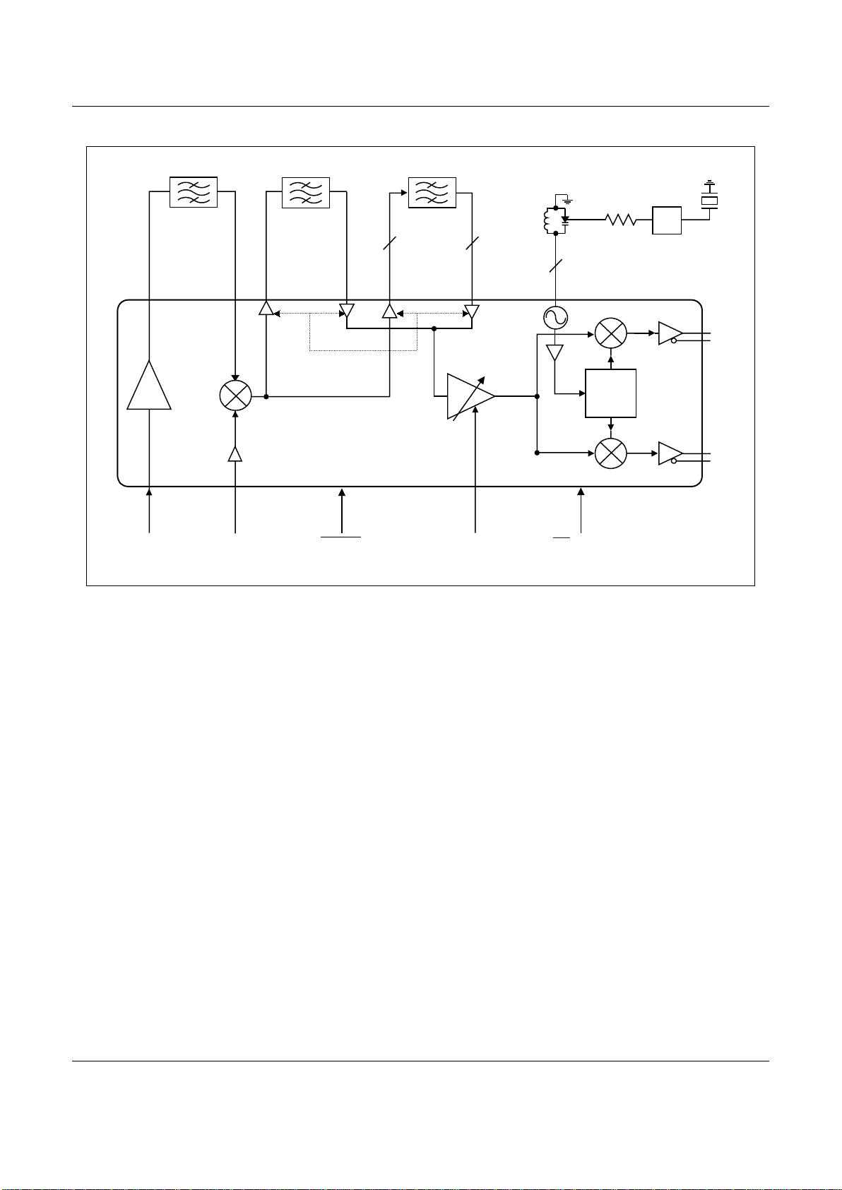
The RF25A device includes the following functional blocks:
• Low Noise Amplifier (LNA)
• RF Downconverted Mixer
• Intermediate Frequency (IF) Variable Gain Amplifier (VGA)
• In-Phaseand Quadrature (I/Q) Demodulator
• Voltage Controlled Oscillator (VCO)
The RF25A Application-Specific Integrated Circuit (ASIC) is a dual-mode,singleband receiver (Rx) intended for use in Code Division Multiple Access(CDMA)
portable phones in thecellular band. It can be used in CDMA mode or Advanced
Mobile Phone System (AMPS) mode.The ASIC provides excellent RF
performance with low DC power dissipation and isassembled in a lowcost, high
performance, 40-pin Land GridArray (LGA) 6 x 6 mm package.
The device incorporates all the components required toimplement the complete
dual-mode receiver front end;from the Low Noise Amplifier (LNA) to the In-Phase
and Quadrature (I/Q) demodulator stages, except for external SAW filters. The LNA
amplifies the incoming signaland outputs to anexternal SAW filter. After filtering,
the signal goes to the mixer for downconversion. The mixer output for the AMPS
mode is single-ended, followedby the external AMPSIntermediate Frequency (IF)
Surface Acoustic Wave (SAW) filter.The mixer output for the CDMA mode mixer
has balanced outputs forexternal IF SAW filtering. The IF SAW filters are followed
by a Variable Gain Amplifier (VGA) and and I/Q demodulator. The mode selection
is controlled by amode control pin.
The IF filter outputs are buffered at the input of the VGA,which has a dynamic
range greater than 90dB.
The on-chip Very High Frequency (VHF) Voltage Controlled Oscillators (VCO)
operates with an externaltank circuit to providethe Local Oscillator (LO) signal for
the I/Q demodulator.
The Gain, Noise Figure(NF), and third order Input Intercept (IIP3) of each stage in
the receiver chip are optimized to meet the system requirements for AMPSand
CDMA modes according to the TIA/EIA 98-B standard. Employingsilicon bipolar
technology, the ASIC is designed for high performance with a high level of
integration and provides acost-effective RF solution for dual-mode phone
applications
The RF25A pin-out is shown in Figure 1,a functional block diagramis illustrated in
Figure 2, and aschematic diagram in Figure 3.
Features
• Dual-Mode Operation
• Battery operation 2.7 to 3.6 V
• High level of integration
• Differential I/Qoutputs for baseband interfaces
• On-chip 100 to 600MHzVCO
• Low DC consumption: < 60 mA
• 40-pin Land Grid Array (LGA)6x6mmpackage
Applications
• CDMA and AMPS handset in the cellular band:
− AMPS
− CDMA (US)
− CDMA (Japan)
Figure 1.RF25ARx ASICPin-out
40-Pin LGA Package
C506
NC
LNA_DECOUPLE
NC
LNA_IN
VCC_RFBIAS
BIAS_SET
FM/CDMA
VCC_VCO
GND
TANK-
TANK+
31
30
29
28
27
26
25
24
23
22
21
NC
DIV2/DIV4
PLL+
Q+
Q-
SLEEP
PLL-
I+
I-
403938
343332
373635
NC
LNA_OUT
NC
VCC_MIXNCLO_IN
MIXEMIT
IF_TRAP
MIX_IN
121314
181920
151617
NC
NC
AMPS_MIXEROUT
CDMA_MIXEROUT-
CDMA_MIXEROUT+
MIX_BYPASS
VGA_AMPS_IN
VGA_CDMA_IN-
VGA_CDMA_IN+
VCC_IF
VGA_CONTROL
1
2
3
4
5
6
7
8
9
10
11
Page 2
RF25A Rx ASIC
2 Conexant – Preliminary. 1011110A
Proprietary Information August 4, 2000
÷ 2,4
AMPS IF SAW
CDMA IF SAW
I
Q
RF25A
Rx ASIC
RF SAW(CELL)
PLL
LNA_IN
4
39
35
29
25
27,28
23,24
14,15
16
17
18
19
C507
LO_IN VGA_CONTROL
22
2
721
7
20
FM/CDMA
SLEEP
32
Figure 2. RF25ARxASIC Block Diagram
Page 3

Rx ASIC RF25A
101110A Conexant – Preliminary 3
August 4, 2000 Proprietary Information
Technical Description
Low Noise Amplifier (LNA). The LNA is designed with a high
gain, low noise figure,and high 3
rd
order input intercept (IIP3)
performance. These parameters canbe optimized with the
mixer gain, noise figure, and IIP3 to achieve the cascade NF
and IIP3 system requirements.RF25A pin 2 isLNA decoupled,
requiring a RF bypasscapacitor to ground with minimal trace
length. Input and outputmatching networks are externalto the
Rx ASIC.
Mixers. The active doublebalanced mixer is designed for high
gain, a low noise figure, and high IIP3performance. The mixer
can also be optimizedfor RF performance to complement the
LNA RF performance, andsatisfy overall Rx NFand IIP3 system
requirements. The LO portoperates with a typicalLO drive level
of -10 dBm. Themixer has a balanced output to drive the IF
SAW filter in CDMA mode, and single-ended output to drive the
IF SAW filter in the AMPS mode.
Variable Gain Amplifier (VGA). Thehigh dynamic range
required by a CDMAhandset is achieved bythe VGA, which has
a minimum dynamic rangeof 90 dB anda control voltage range
from 0.5 to 2.5V. The VGA is common in both modes (CDMA
and AMPS) by switching its internal input buffers.
I/Q Demodulator. The I/Q Demodulator is designed for mobile
handset application. It hasan on-chip generated VHFLO with a
typical operating range of100 to 600 MHz and a typical I/Q
output operating range of 0 to 5 MHz. The I/Q Demodulator is
internally connected to theVGA output, and is fully differential to
reduce common mode noise.DC offsets between differentialI/Q
outputs, and between Iand Q channels, are extremely low to
facilitate compatibility with basebandinterfaces. The
I/Q Demodulator is alsodesigned to have very low amplitude
and phase imbalance.
VHF Oscillator. With external tankcircuits, the VCO p rovides
the LO signal to drive the demodulator, andthe prescaler of an
external Phase Locked Loop (PLL). The oscillator can operate
at two or four times at twice the IF frequency. Usinga selectable
divide ratio, the LOfor the I/Q demodulator is derived. The logic
signal to select thedivider ratio (2 or 4) is available on Pin 13
(DIV2/DIV4).
Mode Control. The operation of the chip is controlled by signals
at Pin 7 (FM/CDMA), Pin 20 (SLEEP), and Pin 13 (DIV2/DIV4).
All the switching is done internally. The supplyvoltage should be
present at all the VCC pins for normal operation. The modes
selected are shown inTable 4.
Electrical and Mechanical Specifications
Included in this documentare Tables 1 through 5 and Figures 1
through 4, which defineand illustrate the electrical and
mechanical specifications of the RF25A.
Table 1: RF25A Pin Assignments and Signal
Descriptions
Table 2: Absolute Maximum Ratings
Table 3: Recommended Operating Conditions
Table 4: Mode Control Select SignalSwitching
Table 5: RF25A RX ASIC Electrical Specifications
Figure 1: RF25A Rx ASIC Pin-out - 40-Pin LGA
6x6mmPackage
Figure 2: RF25A Rx ASIC Block Diagram
Figure 3 – 19: Typical Functional Block Performance
Figure 20: RF25A Schematic Diagram
Figure 21: RF25A Package Dimensions – 40-PinLGA
6x6mmPackage
Figure 22: 40-Pin LGA Tape and Reel Dimensions
ESD Sensitivity
The RF25A is a Class 1 device. The following extreme
Electrostatic Discharge (ESD) precautions arerequired
according to the HumanBody Model (HBM):
• Protective outer garments.
• Handle device in ESD safeguarded work area.
• Transport device in ESD shielded containers.
• Monitor and test all ESDprotection equipment.
The HBM ESD withstand threshold value, with respect to
ground, is ±1.5 kV.The HBM ESD withstand threshold value,
with respect to VDD(the positive power supplyterminal) is also
±1.5 kV.
Page 4
RF25A Rx ASIC
4 Conexant – Preliminary. 1011110A
Proprietary Information August 4, 2000
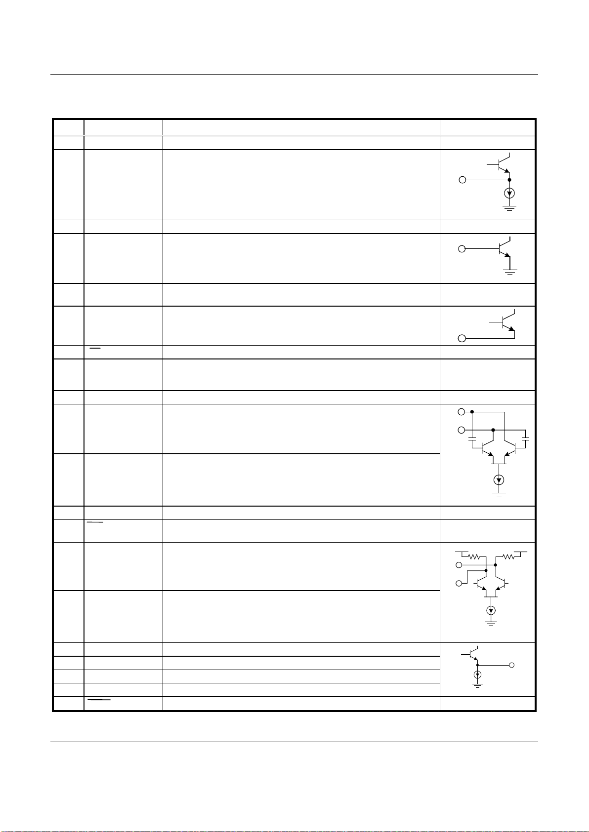
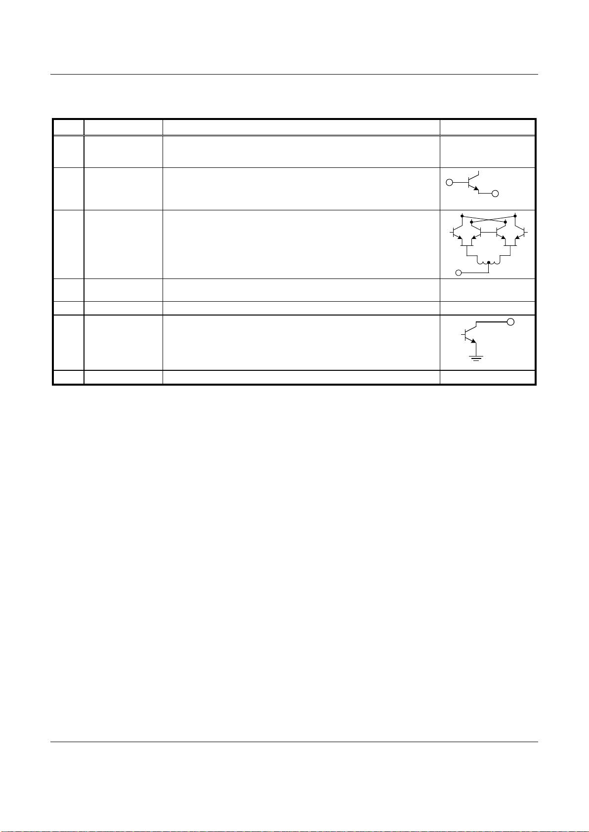
Table 1. RF25A Pin Assignments and Signal Descriptions (1 of 3)
Pin # Name Description Equivalent Circuit
1 NC No connection.
2 LNA_DECOUPLE An RFbypasscapacitor(1000pF) with veryshorttrace shouldbeconnected tothispin.
3 NC No connection
4 LNA_IN The inputto LNAneedsexternal matching.The matching networkshouldbeplaced asclose
to thispin as possible.High Q componentsarerecommended to minimizethe effect onthe
noisefigure.A DC blockingcapacitor isnecessaryatthe input.
5 VCC_RFBIAS Supplyvoltageto the RFbias.An RF bypasscapacitorshouldbeconnectedfromthe pin to
ground withshort traces.
6 BIAS_SET
This pin sets thecellularRFbiascurrent.Typically,a180Ω resistoris connectedfromthe pin
to ground.
7 FM/CDMA Cellularbandmode select: 0=AMPS; 1 = CDMA.
8 VCC_VCO Voltagesupplypin to theVCObuffer. A bypasscapacitor shouldbeplaced closetothe device
frompin8 to pin 9.Thetrace shouldbeshortandconnected immediatelytothe ground plane
forbestperformance.
9 GND Ground returnfrom the VCObuffer.
10 TANK- Differentialtank connectionforthe cellularbandVCO. Care shouldbetaken during thelayout
of the external tank circuit toprevent parasitic oscillations.
11 TANK+ Differentialtank connectionforthe cellularbandVCO. Care shouldbetaken during thelayout
of the external tank circuit toprevent parasitic oscillations.
–
+
12 NC No connection.
13 DIV2/DIV4 Selectsthedivide ratio ofthe VCOtothe LO portofthe I/Q demodulator:0 = divideby2,
1 =divideby40.
14 PLL+ Differentialbuffered VCO output
15 PLL- Differentialbuffered VCOoutput
–
+
VccVcc
16 I+ I channeldifferential output.
17 I- I channeldifferential output.
18 Q+ Q channeldifferentialoutput.
19 Q- Q channeldifferential output.
20 SLEEP Activatessleepmode:0= sleep;1=enable
Page 5
Rx ASIC RF25A
101110A Conexant – Preliminary 5
August 4, 2000 Proprietary Information
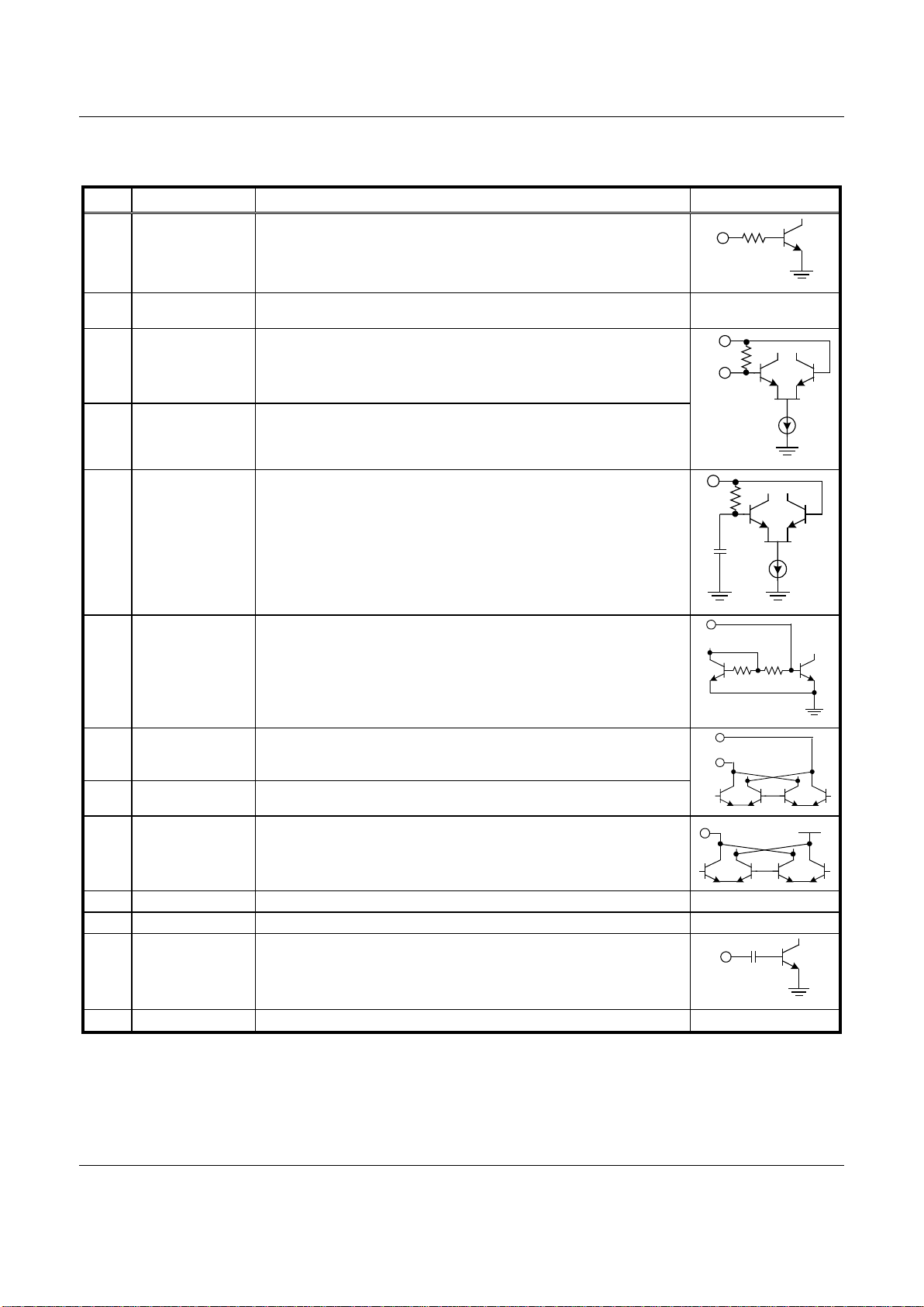
Table 1. RF25A Pin Assignments and Signal Descriptions (2 of 3)
Pin # Name Description Equivalent Circuit
21 VGA_CONTROL
VGA voltageinput. Input impedanceis greater than50KΩ.
22 VCC_IF Voltagesupplyto VGA andI/Qdemodulator stages.Supplyshould be wellregulated and
bypassedtoprevent modulationofthe signal bythe supply ripple.
23 VGA_CDMA_IN+ CDMA differentialVGA input
24 VGA_CDMA_IN- CDMA differentialVGA input
–
+
25 VGA_AMPS_IN AMPS VGAinput.
26 MIX_BYPASS Low frequencybypass fortheamps mixer.
27 CDMA_MIXEROUT+ CDMA differential mixeroutput. Requiresanexternal inductortoVCC. An externalmatch sets
outputimpedance.
28 CDMA_MIXEROUT- CDMAdifferentialmixer output.Requiresan external inductorto VCC. Anexternalmatch sets
outputimpedance.
–
+
29 AMPS_MIXEROUT AMPSmixer output.Requiresan externalinductorto VCC. Anexternalmatchsets output
impedance.
Vcc
30 NC No connection.
31 NC No connection.
32 LO_IN The mixerlocal oscillatorinput drive istypically–10dBm.
33 NC No connection.
Page 6
RF25A Rx ASIC
6 Conexant – Preliminary. 1011110A
Proprietary Information August 4, 2000
Table 1. RF25A Pin Assignments and Signal Descriptions (3 of 3)
Pin # Name Description Equivalent Circuit
34 VCC_MIX Voltagesupplypin for themixers.AnRF bypass capacitorshould be connectedfrom thispin
to ground.It should beconnected asclose to thedeviceaspossible withveryshort trace
lengths.
35 MIX_IN Cellularmixerinput.
Pin 37
36 IF_TRAP The parallelLC circuitistuned to thecellularIFfrequency.
37 MIXEMIT Typicalground connection,buta 1.5 nHemitterdegeneration canbeused toimprovemixer
inputIP3.
See Pin35
38 NC No connection.
39 LNA_OUT Thisisan open collectorLNA output. Aninductormust be connectedto VCC. Thematchingis
done externallyto the chip.
40 NC No connection.
Page 7

Rx ASIC RF25A
101110A Conexant – Preliminary 7
August 4, 2000 Proprietary Information
Table 2.Absolute MaximumRatings
Parameter Minimum Maximum Units
Supplyvoltage(VCC) -0.3 5.0 V
Inputvoltagerange -0.3 VCC V
LNA inputpower +5 dBm
Power dissipation 600 mW
Operatingtemperature -30 +80 °C
Storagetemperature -40 +125 °C
Table 3.Recommended OperatingConditions
Parameter Min Typical Max Units
Supplyvoltage(VCC) 2.7 3.0 3.6 V
Operatingtemperature -30 +25 +80 °C
Impedanceoflogic inputs 50
KΩ
Logic0 0.0 0.5 V
Logic1 VCC -0.5 VCC V
Table 4.ModeControlSelect Signal Switching
Pin # Name AMPS CDMA
7 FM/CDMA 0 1
13 DIV2/DIV4 0 0
20 SLEEP 1 1
Key: 0 =LOW
1=HIGH
Page 8

RF25A Rx ASIC
8 Conexant – Preliminary. 1011110A
Proprietary Information August 4, 2000
Table 5. RF25A Rx ASIC Electrical Specifications (1 of 2)
TA =25°°°° C, VCC=3.0 V, PLO=-10 dBm
Parameter Symbol Test Condition Min Typical Max Units
Cellular LNA
Gain @881MHz 14.5 dB
Gain variation overband (869-894 MHz) 0.5 dB
Gain variation overtemperature 1.5 dB
Noisefigure@ 881 MHz 1.6 dB
Reverse isolation 20 dB
P1dB @input -5 dBm
IP3@input 8dBm
Inputreturnloss (869-894MHz) -12 dB
Outputreturnloss (869-894MHz) -15 dB
Totalsupplycurrent (adjustable) 11 mA
Cellular Mixer
Conversiongain (power):
CDMA mode
AMPS mode
14
11
dB
dB
Single-sidebandnoisefigure:
CDMA mode
AMPS mode
7.5
8
dB
dB
P1dB @input:
CDMA mode
AMPS mode
-6
-9
dBm
dBm
IP3@input:
CDMA mode
AMPS mode
+5
+3
dBm
dBm
MixerRFinput return loss,RF port 1(869-894MHz) -15 dB
LO inputpowerlevel -10 dBm
IF outputresistance:
CDMA mode(differential)
AMPS mode(single-ended)
3000
1000
Ω
Ω
IF frequencyrange 300 MHz
LO/RF inputisolation 20 dB
Totalsupplycurrent (Adjustable) 18 mA
Rx VGA-I/QDemodulator
Frequencyrange 50 300 MHz
Inputimpedance:
CDMA input(differential)
AMPS input(single-ended)
1000
1000
Ω
Ω
Gain:
Maximum
Minimum
Maximum(AMPS)
Minimum(AMPS)
53
–47
61
-39
54
–42
62
–34
55
–37
63
-29
dB
dB
dB
dB
Page 9

Rx ASIC RF25A
101110A Conexant – Preliminary 9
August 4, 2000 Proprietary Information
Table 5. RF25A Rx ASIC Electrical Specifications (2 of 2)
TA =25°°°° C, VCC=3.0 V, PLO=-10 dBm
Parameter Symbol Test Condition Min Typical Max Units
Rx VGA-I/QDemodulator(continued)
Gain slope 45 dB/V
Gain slopelinearity (overany6 dB segment) -3 +3 dB
IF amplifier IIP3:
@ Maximumgain (CDMA mode)
@ Maximumgain (AMPS mode)
-50
-58 dBm
Input1dBcompression @minimum gain -10 dBm
IF amplifiernoise figure:
@ MaximumCDMA gain
@ MinimumCDMA gain
@ MaximumAMPS gain
6
50
8
dB
dB
dB
Output level:
CDMA
AMPS
2.75
5.5
mVrms
mVrms
Maximumoutputlevel 1.4 Vp-p
Gain variation overfrequency:
CDMA (1-630kHz)
AMPS (0.1-12.2kHz)
0.1
0.1
0.3
0.3
dB
dB
I+, I-,andQ+,Q-DC offset 6mVrms
I/Q gain mismatch 0.2 0.3 dB
I/Qphasemismatch 2 4 deg
I toQDCoffset 30 mV
Totalsupplycurrent (includesI/Q mixers,LObuffers, and
dividers)
12 mA
Oscillator
Frequencyrange 100 600 MHz
Phasenoise(fc = 200MHz,unloaded Q =20)@ 100 kHz
offset
-117 dBc/Hz
Secondharmonicdistortion (application dependent) -30 -26 dBc
Outputlevelto PLL (differential) 300 mVp-p
Outputimpedanceto PLL (differential) 300
Ω
Reverse isolation -30 -40 dB
Totalsupplycurrent 8mA
Page 10

RF25A Rx ASIC
10 Conexant – Preliminary. 1011110A
Proprietary Information August 4, 2000
11
11.5
12
12.5
13
13.5
14
14.5
15
15.5
16
2.62.833.23.4
Vcc
Gain [dB]
-30C
25C
80C
Figure 3. Cellular LNA Gain @ 881 MHz
0
0.5
1
1.5
2
2.5
3
3.5
4
2.6 2.8 3 3.2 3.4
Vcc
NF [dB]
-30C
25C
80C
Figure 4. Cellular LNA Noise Figure @ 881 MHz
0
1
2
3
4
5
6
7
8
9
10
2.62.833.23.4
Vcc
IIP3 [dBm]
-30C
25C
80C
Figure 5. Cellular LNA IIP3 @ 881 MHz
0
2
4
6
8
10
12
14
2.62.833.23.4
Vcc
Gain [dB]
-30C
25C
80C
Figure 6. AMPSMixerGain
(RF Frequency = 881.52 MHz, LO Frequency = 966.90 MHz,
IF Frequency=85.38MHz)
0
2
4
6
8
10
12
2.6 2.8 3 3.2 3.4
Vcc
NF [dB]
-30C
25C
80C
Figure 7. AMPSNoise Figure
(RF Frequency = 881.52 MHz, LO Frequency = 966.90 MHz,
IF Frequency=85.38MHz)
0
1
2
3
4
5
6
7
8
9
2.6 2.8 3 3.2 3.4
Vcc
IIP3 [dBm]
-30C
25C
80C
Figure 8. AMPSMixer IIP3
(RF Frequency = 881.52 MHz, LO Frequency = 966.90 MHz,
IF Frequency=85.38MHz)
Page 11

Rx ASIC RF25A
101110A Conexant – Preliminary 11
August 4, 2000 Proprietary Information
5
7
9
11
13
15
17
2.6 2.8 3 3.2 3.4
Vcc
Gain [dB]
-30C
25C
80C
Figure 9. CDMAMixer Gain
(RF Frequency = 881.52 MHz, LO Frequency = 966.90 MHz,
IF Frequency=85.38MHz)
5
6
7
8
9
10
2.6 2.8 3 3.2 3.4
Vcc
NF [dB]
-30C
25C
80C
Figure 10.CDMAMixer NoiseFigure
(RF Frequency = 881.52 MHz, LO Frequency = 966.90 MHz,
IF Frequency=85.38MHz)
0
1
2
3
4
5
6
7
8
2.6 2.8 3 3.2 3.4
Vcc
IIP3 [dBm]
-30C
25C
80C
Figure 11. CDMA Mixer IIP3
(RF Frequency = 881.52 MHz, LO Frequency = 966.90 MHz,
IF Frequency=85.38MHz)
-60
-40
-20
0
20
40
60
0123
Vctrl [V]
Gain [dB]
-30C
25C
80C
Figure 12. CMDA VGA + I/Q Gain vs. Temperature
(IF Frequency=85.38MHz)
-60
-40
-20
0
20
40
60
80
0123
Vctrl[V]
Gain [dB]
2.7V
3.0V
3.3V
Figure 13.CDMAVGA+ I/Q Over Supply
(IF Frequency=85.38MHz)
55
56
57
58
59
60
61
62
63
64
65
2.6 2.8 3 3.2 3.4
Vcc
Gain [dB]
-30C
25C
80C
Figure 14.VGA+I/QGain in AMPSMode
(Vcontrol=2.5V,Frequency = 85.38MHz)
Page 12

RF25A Rx ASIC
12 Conexant – Preliminary. 1011110A
Proprietary Information August 4, 2000
-60
-58
-56
-54
-52
-50
2.6 2.8 3 3.2 3.4
Vcc
IIP3 [dBm]
-30
25
80
Figure 15.VGA+I/QIIP3 inAMPSMode
(Vcontrol=2.5V,Frequency = 85.38MHz)
50
51
52
53
54
55
56
57
58
59
60
2.6 2.8 3 3.2 3.4
Vcc
Gain [dB]
-30C
25C
80C
Figure 16.VGA+I/QGain in CDMAMode
(Vcontrol=2.5V,Frequency = 85.38MHz)
-50
-49
-48
-47
-46
-45
-44
-43
-42
-41
-40
2.6 2.8 3 3.2 3.4
-30C
25C
80C
Figure 17.VGA+I/QIIP3 inCDMAMode
(Vcontrol=2.5V,Frequency = 85.38MHz)
0
1
2
3
4
5
6
7
8
9
10
2.6 2.8 3 3.2 3.4
Vcc
NF (dB)
-
30C
25C
80C
Figure 19.VGA+I/QNoise FigureinCDMAMode
(Vcontrol=2.5V,Frequency = 85.38MHz)
5
6
7
8
9
10
11
12
13
14
15
2.6 2.8 3 3.2 3.4
Vcc
NF (dB)
-30C
25C
80C
Figure 18.VGA+I/QNoise FigureinAMPSMode
(Vcontrol=2.5V,Frequency = 85.38MHz)
Page 13

Rx ASIC RF25A
101110A Conexant – Preliminary 13
August 4, 2000 Proprietary Information
6.8 nH
A2
1SV306
RX_VCC
RX_TUNE
A1
C2
56 nH56 nH
Cathode 1 Anode 1
Cathode 2 Anode 2
C1
RX_VCC
RXPLL+
RXPLL–
FM
800_LNA_IN
RX_VCC
RX_LO_800
RX_VCC
RX_AGC_ADJ
RXQ–
RXQ+
RXI–
RXI+
TO RF IMAGE
FILTER INPUT
FROM RF IMAGE
FILTEROUTPUT
RX_VCC
RX_VCC
DNI
33 pF
1000 pF
3.3 pF
33 pF
10
50 ohms
50 ohms
50 ohms
1nF1nF
1K
33 pF 180 1000 pF
5.1
220 pF 1000 pF5.1
4700 pF 4700 pF
33 pF33 pF 5.15.1
2KDNI
DNI
1000 pF
1000 pF
180 nH
1.5 nH
10
DNI
33 pF
1K
390 nH
3900 pF 0.1µF
1.5 K
39 nH
0.1 µF 1000 pF
0.1 µF 3900 pF
1000 pF
10
1K
1K
0
0
0
RX_VCC
10
SLEEP
33 pF 0.1 µF
NOTES:
1. COMPONENT VALUES MAY CHANGE
2. DNI =DO NOT INSTALL
0
RF25A
NC
NC
IF_TRAP
MIX_IN
MIXEMIT
NC
LO_IN
NC
TANK+
I+
PLL–
I–
Q+
Q–
DIV2/DIV4
SLEEP
LNA_DECOUPLE
NC
NC
LNA_IN
VCC1
BIAS_SET
FM_CDMA
VCC2
GND
AMPS_IF_OUT
NC
CDMA_IF_OUT–
CDMA_IF_OUT+
MIX_BYPASS
VGA_CDMA_IN–
VGA_CDMA_IN+
VCC3
VGA_CONTROL
11
1
2
3
4
5
6
7
8
9
10
21
31
30
29
28
27
26
25
24
23
22
121314151617181920
403938373635343332
VGA_AMPS_IN
NC
VCC4
PLL+
TANK–
LAN_OUT
FROM CDMA
IF SAW OUTPUT
FROM AMPS IFSAW OUTPUT
3900 pF
3900 pF
3900 pF
DNI 33 pF
4.7 nF
TO CDMA
IF SAW INPUT
TO AMPS IF SAWINPUT
RX_VCC
DNI
39 nH
1.5 K
33 pF 0.1 µF
18 pF
Figure 20.RF25ASchematicDiagram
Page 14

RF25A Rx ASIC
14 Conexant – Preliminary. 1011110A
Proprietary Information August 4, 2000
C822
All dimensions are in millimeters
Pin #1
6.0 ± 0.05
0.500
0.300 ± 0.05
0.355 ± 0.05
1.36 ± 0.10
0.35 ± 0.05
2.936
R1.500
2.936
Solder Mask
Pin #1 Mark
Pin #1
Downset Paddle
Mold
Substrate
6.0 ± 0.05
Figure 21. RF25A Package Dimensions - 40-pin LGA 6 x 6mm Package
Page 15

Rx ASIC RF25A
101110A Conexant – Preliminary 15
August 4, 2000 Proprietary Information
7˚ MAX
6.35
1.59
6.35
1.75
1.50
4.00
8.00
5.50
1.50 ± 0.25
0.292 ± 0.02
12.00 +0.30/-0.10
8˚ MAX
NOTES:
1. Carrier Tape Material: Black Conductive Polycarbonate
2. Cover Tape Material: Transparent Conductive PSA
3. Cover Tape Size: 9.3 mm width
4. Tolerance: .XX = ± 0.10
5. All dimensions are in millimeters
CNXT022
A0 B0K0
Figure 22.40-pinLGATape and Reel Dimensions
Page 16

RF25A Rx ASIC
16 Conexant – Preliminary. 1011110A
Proprietary Information August 4, 2000
Ordering Information
Model Name ManufacturingPart
Number
ProductRevision
RF25A RF25A-12 12
©2000,Conexant Systems,Inc.All RightsReserved.
Informationin this documentisprovided inconnectionwithConexant Systems,Inc.("Conexant")products.Thesematerials areprovidedby Conexantasa service toits
customersandmay be usedforinformational purposesonly.Conexant assumesnoresponsibilityforerrors oromissionsinthesematerials.Conexant maymakechanges to
specificationsandproductdescriptionsatany time,withoutnotice. Conexantmakesnocommitmenttoupdate the informationand shall havenoresponsibility whatsoever
forconflictsor incompatibilitiesarising fromfuture changesto its specificationsand product descriptions.
No license,express orimplied,byestoppel or otherwise,to any intellectualpropertyrights isgrantedbythis document.Exceptas providedinConexant’s Termsand
ConditionsofSale for suchproducts,Conexantassumes no liabilitywhatsoever.
THESE MATERIALSAREPROVIDED "AS IS" WITHOUTWARRANTYOF ANY KIND,EITHEREXPRESS OR IMPLIED, RELATINGTOSALE AND/OR USE OF
CONEXANT PRODUCTSINCLUDINGLIABILITY OR WARRANTIESRELATINGTO FITNESS FOR APARTICULARPURPOSE, CONSEQUENTIAL ORINCIDENTAL
DAMAGES, MERCHANTABILITY,OR INFRINGEMENT OF ANYPATENT,COPYRIGHT OR OTHER INTELLECTUALPROPERTYRIGHT. CONEXANT FURTHER
DOES NOTWARRANTTHE ACCURACY OR COMPLETENESS OFTHEINFORMATION, TEXT, GRAPHICSOROTHER ITEMS CONTAINED WITHINTHESE
MATERIALS.CONEXANTSHALLNOT BE LIABLE FORANYSPECIAL, INDIRECT, INCIDENTAL,ORCONSEQUENTIAL DAMAGES, INCLUDINGWITHOUT
LIMITATION,LOSTREVENUES OR LOST PROFITS,WHICHMAY RESULT FROM THEUSEOF THESE MATERIALS.
Conexantproductsare not intendedforuse in medical,lifesavingor life sustainingapplications.Conexantcustomers usingorselling Conexant products foruseinsuch
applicationsdo so at theirown risk andagreeto fullyindemnifyConexant foranydamages resultingfromsuch improperuseor sale.
The followingare trademarksofConexant Systems,Inc.:Conexant™,theConexant C symbol,and “What’s Nextin CommunicationsTechnologies”™.Productnames or
serviceslisted inthispublication areforidentificationpurposesonly,and may be trademarksofthird parties.Third-partybrandsand names arethe propertyof their
respectiveowners.
Additionalinformation,postedatwww.conexant.com
, isincorporated byreference.
Reader Response:Conexantstrivestoproduce qualitydocumentationandwelcomesyourfeedback. Pleasesend commentsand suggestionsto
tech.pubs@conexant.com.Fortechnical questions,contact yourlocalConexantsales officeorfield applicationsengineer.
Page 17

Further Information
literature@conexant.com
(800) 854-8099 (North America)
(949) 483-6996 (International)
Printed inUSA
World Headquarters
Conexant Systems, Inc.
4311 Jamboree Road
Newport Beach, CA
92660-3007
Phone: (949) 483-4600
Fax 1: (949) 483-4078
Fax 2: (949) 483-4391
Americas
U.S. Northwest/
PacificNorthwest – SantaClara
Phone: (408) 249-9696
Fax: (408) 249-7113
U.S. Southwest – Los Angeles
Phone: (805) 376-0559
Fax: (805) 376-8180
U.S. Southwest – Orange County
Phone: (949) 483-9119
Fax: (949) 483-9090
U.S. Southwest –San Diego
Phone: (858) 713-3374
Fax: (858) 713-4001
U.S. North Central– Illinois
Phone: (630) 773-3454
Fax: (630) 773-3907
U.S. South Central – Texas
Phone: (972) 733-0723
Fax: (972) 407-0639
U.S. Northeast – Massachusetts
Phone: (978) 367-3200
Fax: (978) 256-6868
U.S. Southeast– North Carolina
Phone: (919) 858-9110
Fax: (919) 858-8669
U.S. Southeast –Florida/
SouthAmerica
Phone: (727) 799-8406
Fax: (727) 799-8306
U.S. Mid-Atlantic – Pennsylvania
Phone: (215) 244-6784
Fax: (215) 244-9292
Canada – Ontario
Phone: (613) 271-2358
Fax: (613) 271-2359
Europe
Europe Central – Germany
Phone: +49 89 829-1320
Fax: +49 89 834-2734
Europe North– England
Phone: +44 (0)118 920 9500
Fax: +44 (0)118 9209595
Europe –Israel/Greece
Phone: +972 9 9524000
Fax: +972 9 9573732
Europe South– France
Phone: +33141443651
Fax: +33141443690
Europe Mediterranean –Italy
Phone: +39 02 93179911
Fax: +39 02 93179913
Europe – Sweden
Phone: +46 (0) 8 50914319
Fax: +46 (0) 8590 041 10
Europe – Finland
Phone: +358 (0) 9 85666 435
Fax: +358 (0) 985 666 220
Asia – Pacific
Taiwan
Phone: (886-2) 2-720-0282
Fax: (886-2) 2-757-6760
Australia
Phone: (61-2) 9869 4088
Fax: (61-2) 9869 4077
China–Central
Phone: 86-21-6361-2515
Fax: 86-21-6361-2516
China–South
Phone: (852) 2 827-0181
Fax: (852) 2 827-6488
China – South (Satellite)
Phone: (86) 755-518-2495
China–North
Phone: (86-10) 8529-9777
Fax: (86-10) 8529-9778
India
Phone: (91-11) 692-4789
Fax: (91-11) 692-4712
Korea
Phone: (82-2) 565-2880
Fax: (82-2) 565-1440
Korea (Satellite)
Phone: (82-53) 745-2880
Fax: (82-53) 745-1440
Singapore
Phone: (65) 737 7355
Fax: (65) 737 9077
Japan
Phone: (81-3) 5371 1520
Fax: (81-3) 5371 1501
 Loading...