

Page 1
RF212
Image-Reject Front End for Dual or Tri-Band GSM Applications
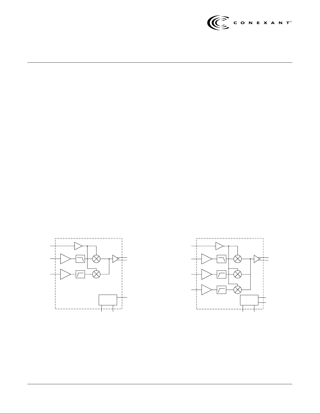
The RF212 device is available as a dual-band (EGSM900/DCS1800) front end or
as a tri-band (EGSM900/DCS1800/PCS1900) front end for Global System for
Mobile Communications (GSM) mobile telephony applications. Each device
integrates all the required front-end components after the frequency pre-select
filters. These components include the Low Noise Amplifiers (LNAs), the internal
image-reject filters, mixers, and a Local Oscillator (LO) amplifier.
The main advantage of the RF212 is its ability to provide a minimum of 35 dB of
image rejection for each band. The block diagrams of the devices are shown in
Figures 1 and 2. The device packages and pin configurations are shown in Figures
3 and 4.
Features
• Supports EGSM
• LNA and mixer for RF to IF conversion
• 12 dB or 20 dB switchable gain step
• Minimum 35 dB of image rejection
• No external post-LNA filters required
• Common Intermediate Frequency (IF) port for all
bands
• IF range from 350 MHz to 450 MHz
• High isolation LO input buffer
• Differential IF output
• High dynamic range with low current consumption
• Three-cell battery operation (2.7 to 3.6 V)
• 20-pin Exposed paddle, Thin Shrink Small Outline
Package (ETSSOP)
Applications
• Dual/tri-band digital cellular mobile telephony
(EGSM900/DCS1800, or
EGSM900/DCS1800/PCS1900)
LOIN
LNA900IN IFout
LNA1800IN
control
Gain
Step
Sel
Sel
Figure 1. RF212 Dual-Band Device Block Diagram
Data Sheet
Proprietary Information and Specifications are Subject to Change May 24, 2000
Band Select 1
C0002
Conexant
LOIN
LNA900IN IFout
LNA1800IN
LNA1900IN
Band Select 1
Band Select 2
Sel
Step
Sel
control
Gain
Figure 2. RF212 Tri-Band Device Block Diagram
Doc. No. 100780D
C0001
Page 2
RF212 Image-Reject Front End
GND
GND
LNA900IN
VCC
VCC
GAINSEL
LNA1800IN
GND
ENA
NC
1
2
3
4
5
6
7
8
9
10
VCC
20
GND
19
STEPSEL
18
IFOUT+
17
IFOUT-
16
GND
15
BANDSEL1
14
LOIN
13
LOGND
12
NC
11
C067
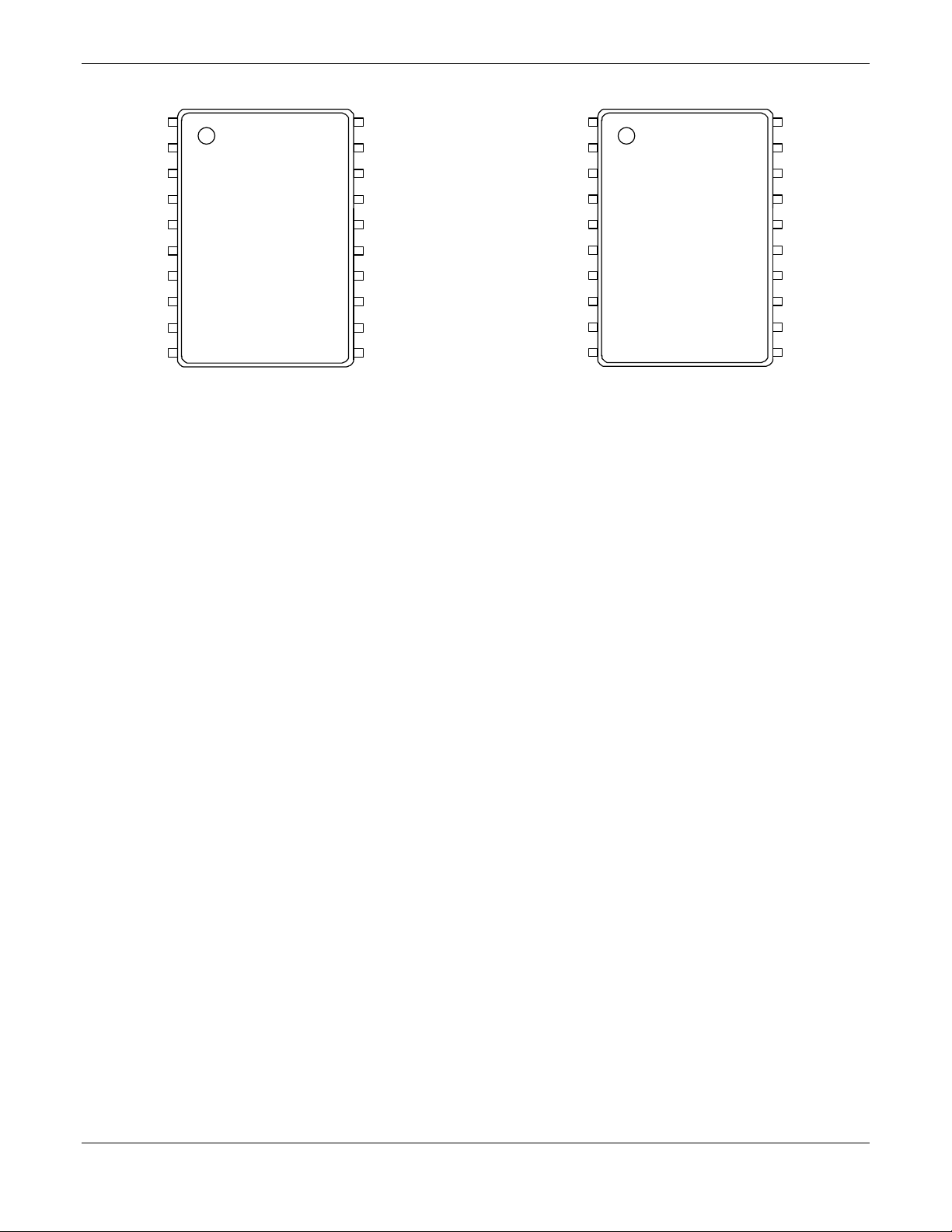
Figure 3. RF212 Dual-Band Device Pin Configuration −−−− 20-Pin
ETSSOP
Technical Description
Both RF212 devices form front ends of a dual-band or a tri-band
super-heterodyne receiver. The RF212 dual-band device is
optimized for an EGSM900/DCS1800 design, while the RF212
tri-band device is suitable for EGSM900, DCS1800, and PCS
1900. Each frequency band has its own separate front-end
receiver path. Each receiver path contains an LNA, an imagereject filter, and a mixer. The IF and LO ports are common to all
frequency bands. The image rejection achievable by this frontend design without any additional external components is 35 dB
minimum for an IF of 400 MHz. Both devices operate over a
supply voltage range of 2.7 V to 3.6 V.
The RF212 dual-band device has one band selection pin
(BANDSEL1 on pin 14). When BANDSEL1 is set to logic “0,” the
EGSM900 receiver path is active. The LO frequency needs to
be higher than the RF input frequency (i.e., a high side injection
is used). When BANDSEL1 is set to logic “1,” the DCS1800
receiver path is active. The LO frequency needs to be less than
the RF input frequency (i.e., a low-side injection is used). With a
400 MHz IF, this arrangement allows a single, wide-range
Voltage Controlled Oscillator (VCO) to be used for each band of
operation.
GND
GND
LNA900IN
VCC
VCC
GAINSEL
LNA1800IN
LNA1900IN
ENA
NC
1
2
3
4
5
6
7
8
9
10
VCC
20
GND
19
STEPSEL
18
IFOUT+
17
IFOUT-
16
BANDSEL2
15
BANDSEL1
14
LOIN
13
LOGND
12
NC
11
C122
Figure 4. RF212 Tri-Band Device Pin Configuration – 20-Pin
ETSSOP
Similarly, the RF212 tri-band device has two band selection pins
(BANDSEL1 and BANDSEL2, pins 14 and 15, respectively). The
EGSM900 path uses the high side injection for the LO, while
DCS1800 and PCS1900 paths use the low side injection. Tables
1 and 2 provide the frequency band selection settings for the
dual and tri-band devices, respectively.
All the LNAs have switchable gain. The gain mode is selectable
using the GAINSEL signal (pin 7). Low gain mode is selected by
driving the GAINSEL signal to a logic “1”; high gain mode is
selected by driving the signal to a logic “0.” Depending on the
need of the handset design on the gain distribution, the gain
step between the high gain and low gain modes can be set to
either a 12 dB step or a 20 dB step. This gain step is selectable
with the STEPSEL signal (pin 18).
Electrical and Mechanical Specifications________________
The RF212 signal pin assignments and functional pin
descriptions are found in Table 3 (dual-band) and Table 4 (triband). The absolute maximum ratings of the RF212 are
provided in Table 5, the operating conditions are specified in
Table 6, and electrical specifications are provided in Table 7.
Figure 3 shows the diagram for a typical application circuit using
the RF212 front end. Figure 4 provides the package dimensions
for both of the 20-pin ETSSOP devices.
ESD Sensitivity
The RF212 is a static-sensitive electronic device. Do not operate
or store near strong electrostatic fields. Take proper ESD
precautions.
2
May 24, 2000 Proprietary Information and Specifications are Subject to Change
Conexant
100780D
Page 3
Image-Reject Front End RF212
Table 1. RF212 Dual-Band Selection
BANDSEL1, pin 14 Mode
0 EGSM900
1 DCS1800
Table 2. RF212 Tri-Band Selection
BANDSEL1, pin 14 BANDSEL2, pin 15 Mode
0
0
1 0 DCS1800
1 1 PCS1900
0
1
EGSM900
Table 3. RF212 Dual-Band Device Signal Description
Pin # Name Description Pin # Name Description
1 NC No connect (recommend c onnecting to
ground)
2 GND Ground 12 LOGND LO input ground
3 GND Ground 13 LOIN LO input
4 LNA900IN 900 MHz LNA input 14 BANDSEL1 Band select control
5 VCC Supply 15 GND Ground
6 VCC Supply 16
7 GAINSEL LNA gain select 17 IFOUT+ Mixer posi tive output
8 LNA1800IN 1800 MHz LNA input 18 STEPSEL Gain step select. STEPSEL= 0 selects a
9 GND Ground 19 GND Ground
10 ENA Device enable, active high 20 VCC Supply
11 NC No connect (recommend c onnecting to
IFOUT−
ground)
Mixer negative output
12 dB gain step; STEPSEL = 1 selec ts a
20 dB gain step
Table 4. RF212 Tri-Band Device Signal Description
Pin # Name Description Pin # Name Description
1 NC No connect (recommend c onnecting to
2 GND Ground 12 LOGND LO input ground
3 GND Ground 13 LOIN LO input
4 LNA900IN 900 MHz LNA input 14 BANDSEL1 Band select control 1
5 VCC Supply 15 BANDSEL2 Band select control 2
6 VCC Supply 16
7 GAINSEL LNA gain select 17 IFOUT+ Mixer posi tive output
8 LNA1800IN 1800 MHz LNA input 18 STEPSEL Gain step select. STEPSEL= 0 selects a
9 LNA1900IN 1900 MHz LNA input 19 GND Ground
10 ENA Device enable, active high 20 VCC Supply
100956A
ground)
Conexant – Preliminary
11 NC No connect (recommend c onnecting to
IFOUT−
ground)
Mixer negative output
12 dB gain step; STEPSEL = 1 selec ts a
20 dB gain step
May 18, 2000 Proprietary Information and Specifications are Subject to Change
3
Page 4

RF212 Image-Reject Front End
Table 5. Absolute Maximum Ratings
Parameter Minimum Maximum Units
Storage Temperature
Supply Voltage (VCC)
Input Voltage Range
−40
−0.3
−0.3
+125 °C
+3.6 V
Vcc V
Table 6. RF212 Recommended Operating Conditions
Parameter Min Typical Max Units
Supply Voltage 2.7 3.0 3.6 V
Operating Temperature
−30
+25 +85
°C
Table 7. RF212 Electrical Specifications (1 of 3)
(TA = 25 °°°°C, Vcc = 2.7 V, f
IF
= 400 MHz, Plo = −−−−10 dBm)
Parameter Symbol Test Condition Min Typical Max Units
EGSM900 Mode
Supply current::
Enable mode
Sleep mode
RF Input frequency 925 960 MHz
IF frequency f
IF
LO to RF input isolation 30 dB
Input impedance 50
Power gain (for 2 kΩ differ ential output impedance):
MAX
High gain mode
Low gain mode 1
Low gain mode 2
Gain step 1
Gain step 2
Temperature coefficient
G
MIN
G
MIN
G
STEP
G
STEP
G
TC
F
Gain variation ver sus frequency
Noise figure:
High gain
Low gain mode 1
Low gain mode 2
Noise figure degradati on with blocker:
High gain
Input 1 dB compression point IP1
D
Input third order i ntercept point IP3
Differential IF shunt output resistance 2
Image rejection:
IF
= 400 MHz
f
IF
= 350 or 450 MHz
f
ENA = 1
ENA = 0
1
GAINSEL = 0
1
GAINSEL = 1, STEPSEL = 1
2
GAINSEL = 1, STEPSEL = 0
1
2
1
GAINSEL = 0
GAINSEL = 1, STEPSEL = 1
GAINSEL = 1, STEPSEL = 0
−22 dBm blocker,
GAINSEL = 0 (Note 1)
B high gain mode
low gain mode
15
30
mA
µA
350 400 450 MHz
Ω
20
–24
–14
22
0
10
–22
–12
–0.02
2.3
18
10
25
–20
–10
dB/°C
0.8
3.5 dB
dB
dB
dB
dB
dB
dB
dB
dB
1.6 dB
−22
−18
–20
–13
−12
dBm
dBm
dBm
kΩ
35
25
50 dB
dB
4
Conexant
May 24, 2000 Proprietary Information and Specifications are Subject to Change
100780D
Page 5

Image-Reject Front End RF212
Table 7. RF212 Electrical Specifications (2 of 3)
(TA = 25 °°°°C, Vcc = 2.7 V, f
IF
= 400 MHz, Plo = −−−−10 dBm)
Parameter Symbol Test Condition Min Typical Max Units
DCS1800 Mode
Supply current:
Enable mode
Sleep mode
RF input frequency 1805 1880 MHz
IF frequency 350 400 450 MHz
LO to RF input isolation 30 dB
Input impedance 50
Power gain (for 2 kΩ differ ential output impedance):
MAX
High gain mode
Low gain mode 1
Low gain mode 2
Gain step 1
Gain step 2
Temperature coefficient
G
MIN
G
MIN
G
STEP
G
STEP
G
TC
F
Gain variation ver sus frequency
Noise figure:
High gain
Low gain mode 1
Low gain mode 2
Noise figure degradati on with blocker:
High gain
Input 1 dB compression point IP1
D
Input third order i ntercept point IP3
Differential IF shunt output resistance 2
Image rejection:
IF
= 400 MHz
f
IF
= 350 or 450 MHz
f
PCS1900 Mode (for tri-band devi ce only)
Supply current:
Enable mode
Sleep mode
RF input frequency 1930 1990 MHz
IF frequency 350 400 450 MHz
LO to RF input isolation 30 dB
Input impedance 50
Power gain (for 2 kΩ differ ential output impedance):
MAX
High gain mode
Low gain mode 1
Low gain mode 2
Gain step 1
Gain step 2
Temperature coefficient
G
MIN
G
MIN
G
STEP
G
STEP
G
TC
F
Gain variation ver sus frequency
Noise figure:
High gain
Low gain mode 1
Low gain mode 2
Noise figure degradati on with blocker:
High gain
ENA = 1
ENA = 0
1
GAINSEL = 0
1
GAINSEL = 1, STEPSEL = 1
2
GAINSEL = 1, STEPSEL = 0
1
2
1
GAINSEL = 0
GAINSEL = 1, STEPSEL = 1
GAINSEL = 1, STEPSEL = 0
−22 dBm blocker,
GAINSEL = 0 (Note 2)
B high gain mode
low gain mode
ENA = 1
ENA = 0
1
GAINSEL = 0
1
GAINSEL = 1, STEPSEL = 1
2
GAINSEL = 1, STEPSEL = 0
1
2
1
GAINSEL = 0
GAINSEL = 1, STEPSEL = 1
GAINSEL = 1, STEPSEL = 0
−22 dBm blocker,
GAINSEL = 0 (Note 3)
20
–22
–14
−23
−20
35
25
20
–22
–14
19
30
22
25
2
10
–20
–12
–18
–10
–0.02
1.2
3.5
4.5 dB
16.5
11
1.6 dB
–20
–16
−12
40 dB
19
30
22
25
2
10
–20
–12
–18
–10
–0.02
1.2
3.5
4.5 dB
16.5
11
1.6 dB
mA
µA
Ω
dB
dB
dB
dB
dB
dB/°C
dB
dB
dB
dBm
dBm
dBm
kΩ
dB
mA
µA
Ω
dB
dB
dB
dB
dB
dB/°C
dB
dB
dB
100956A
Conexant – Preliminary
May 18, 2000 Proprietary Information and Specifications are Subject to Change
5
Page 6

RF212 Image-Reject Front End
Table 7. RF212 Electrical Specifications (3 of 3)
(TA = 25 °°°°C, Vcc = 2.7 V, f
IF
= 400 MHz, Plo = −−−−10 dBm)
Parameter Symbol Test Condition Min Typical Max Units
PCS1900 Mode (for tri-band device only) (continued)
Input 1 dB compression point high gain mode
low gain mode
−23
−20
Input third order i ntercept point
Differential IF shunt output resistance 2
Image rejection:
IF
= 400 MHz
f
IF
= 350 or 450 MHz
f
35
25
Local Oscillator (LO)
LO frequency 1275 1640 MHz
LO input return loss (with external matc hing circuit) fIF = 400 MHz
LO input power P
LO
−15 −10 −5
Control Signals (All Modes)
Digital input volt ages (ENA, GAINSEL, BANDSEL1,
BANDSEL2, and STEPSEL)
Enable time t
IH
V
IL
V
Vcc –
0.4
ON
Bandselect switching time 15
Note 1: Assumes −5 dBm @ 915 MHz blocker at the antenna input attenuated by 17 dB.
Note 2: Assumes −12 dBm @ 1785 MHz blocker at the antenna input attenuated by 10 dB.
Note 3: Assumes −12 dBm @ 1910 MHz blocker at the antenna input attenuated by 10 dB.
–20
–16
−12
40 dB
−10
0.4
10
dBm
dBm
dBm
kΩ
dB
dB
dBm
V
V
µs
µs
cc
V
0
1
p
2
F
7
Bias
2
5
2
3
12
0
0
0
2
p
2
F
2
M
G
filte
x
R
r
S
E
F
p
7
4
n
2
H
1
p
2
F
ilte
R
r
x F
S
C
D
ilte
R
r
x F
S
C
P
1
.5
.0
3
n
0
0
0
2
1
H
.2
1
p
.0
3
n
H
p
2
F
2
L
E
S
IN
G
A
IN
0
0
9
A
N
L
4
IN
0
0
8
1
A
N
L
8
p
F
IN
0
0
9
1
A
N
L
9
F
E
L
B
A
N
E
10
6
Control
19
0
1
p
0
.2
F
1
20
F
2
2
1
L
n
2
H
8
+
T
IF
O
U
17
-
T
IF
O
U
16
1
L
E
S
D
N
A
B
14
15
18
13
2
2
L
E
S
D
N
A
B
L
E
S
P
E
T
S
O
L
IN
L
n
2
H
8
p
0
F
0
1
p
0
0
1
0
0
0
2
p
2
F
0
0
0
2
p
7
F
2
.7
4
to
W
IF
S
A
m
tc
a
F
2
n
h
0
0
0
2
p
2
F
H
)
2
L
+
1
K
|| (L
2
l
iffe
d
tia
re
n
C903
Figure 3. Typical RF212 Application Circuit
(for dual-band device, ground pins 9 and 15)
6
Conexant
May 24, 2000 Proprietary Information and Specifications are Subject to Change
100780D
Page 7

Image-Reject Front End RF212
0.65 mm
1.00 mm Ref
TOP VIEW
4.40±0.10 mm
Pin 1 indicator
123
6.40 mm
base metal
4.20 mm
123
3.0 mm
BOTTOM VIEW
6.50±0.10 mm
0.24+0.06/-0.05 mm
1.00+0.5/-0.2 mm
1.20 mm max
0.10±0.05 mm
END VIEW
Figure 4. RF212 Package Dimensions −−−− 20-Pin ETSSOP
SIDE VIEW
C003
100956A
Conexant – Preliminary
May 18, 2000 Proprietary Information and Specifications are Subject to Change
7
Page 8

RF212 Image-Reject Front End
Ordering Information
Model Name Manufacturing Part
Number
Dual-Band Image-Reject Front End
Tri-Band Image-Reject Front End
RF212-11
RF212-21
© 2000, Conexant Syst ems, Inc. All Rights Reserved.
Information in thi s document is provided in connection with Conexant Systems, Inc. ("Conexant") products. These materials are prov ided by Conexant as a serv ice to its
customers and may be used for informational purposes only. Conexant assumes no responsibility for errors or omissions in these material s. Conexant may make changes to
specifications and product descriptions at any time, without notice. Conexant makes no commitment to update the information and shall have no responsibility whatsoever
for conflicts or incompat ibilities arising from future changes to it s specifications and product descriptions.
No license, express or implied, by estoppel or otherwise, to any intellectual property rights i s granted by this document. Except as provided in Conexant’s Terms and
Conditions of Sale for such pr oducts, Conexant assumes no liability whatsoever.
THESE MATERIALS ARE PROVIDED "AS IS" WITHOUT WARRANTY OF ANY KIND, EITHER EXPRESS OR IMPLI ED, RELATING TO SALE AND/OR USE OF
CONEXANT PRODUCTS INCLUDING LIABILITY OR WARRANTIES RELATING TO FITNESS FOR A PARTI CULAR PURPOSE, CONSEQUENTIAL OR INCIDENTAL
DAMAGES, MERCHANTABILITY, OR INFRINGEMENT OF ANY PATENT, COPYRIGHT OR OTHER INTELLECTUAL PROPERTY RIGHT. CONEXANT FURTHER
DOES NOT WARRANT THE ACCURACY OR COMPLETENESS OF THE INFORMATION, TEXT, GRAPHICS OR OTHER ITEMS CONTAINED WITHI N THESE
MATERIALS. CONEXANT SHALL NOT BE LIABLE FOR ANY SPECIAL, INDIRECT, I NCIDENTAL, OR CONSEQUENTIAL DAMAGES, INCLUDING WITHOUT
LIMITATION, LOST REVENUES OR LOST PROFITS, WHICH MAY RESULT FROM THE USE OF THESE MATERIALS.
Conexant products ar e not intended for use in medical, lifesaving or life sustaining applications. Conexant customers using or selling Conexant products for use in such
applications do so at their own risk and agree to fully indemnify Conexant for any damages resulting from such impr oper use or sale.
The following are trademarks of Conexant Syst ems, Inc.: Conexant™, the Conexant C symbol, and “What’s Next in Communications Technologies”™. Product names or
services l isted in this publication are for identification purposes onl y, and may be trademarks of third parties. Third-party brands and names are the property of thei r
respective owners.
Additional information, posted at www.conexant.com, is incor porated by reference.
Reader Response: Conexant strives to produce qualit y documentation and welcomes your feedback. Please send comments and suggesti ons to
tech.pubs@conexant .com. For technical questions, contac t your local Conexant sales office or f ield applications engineer.
8
Conexant
100780D
May 24, 2000 Proprietary Information and Specifications are Subject to Change
Page 9

Further Information
literature@conexant.com
(800) 854-8099 (North America)
(949) 483-6996 (International)
Printed in U SA
World Headquarters
Conexant S ystems, Inc.
4311 Jamboree Road
Newport Beach, CA
92660-3007
Phone: (949) 483-4600
Fax 1: (949) 483-4078
Fax 2: (949) 483-4391
Americas
U.S. Northwest/
Pacific Northwest – Santa Clara
Phone: (408) 249-9696
Fax: (408) 249-7113
U.S. Southwest – Los Angeles
Phone: (805) 376-0559
Fax: (805) 376-8180
U.S. Southwest – Orange County
Phone: (949) 483-9119
Fax: (949) 483-9090
Europe North – England
Phone: +44 1344 486444
Fax: +44 1344 486555
Europe – Israel/Greece
Phone: +972 9 9524000
Fax: +972 9 9573732
Europe South – France
Phone: +33 1 41 44 36 51
Fax: +33 1 41 44 36 90
Europe Mediterranean – Italy
Phone: +39 02 93179911
Fax: +39 02 93179913
Europe – Sweden
Phone: +46 (0) 8 5091 4319
Fax: +46 (0) 8 590 041 10
Europe – Finland
Phone: +358 (0) 9 85 666 435
Fax: +358 (0) 9 85 666 220
Asia – Pacific
Taiwan
Phone: (886-2) 2-720-0282
Fax: (886-2) 2-757-6760
U.S. Southwest – San Diego
Phone: (858) 713-3374
Fax: (858) 713-4001
U.S. North Central – Illinois
Phone: (630) 773-3454
Fax: (630) 773-3907
U.S. South Central – Texas
Phone: (972) 733-0723
Fax: (972) 407-0639
U.S. Northeast – Massachusetts
Phone: (978) 367-3200
Fax: (978) 256-6868
U.S. Southeast – North Carol ina
Phone: (919) 858-9110
Fax: (919) 858-8669
U.S. Southeast – Florida/
South America
Phone: (727) 799-8406
Fax: (727) 799-8306
U.S. Mid-Atlantic – Pennsylvania
Phone: (215) 244-6784
Fax: (215) 244-9292
Canada – Ontario
Phone: (613) 271-2358
Fax: (613) 271-2359
Europe
Europe Central – Germany
Phone: +49 89 829-1320
Fax: +49 89 834-2734
Australia
Phone: (61-2) 9869 4088
Fax: (61-2) 9869 4077
China – Central
Phone: 86-21-6361-2515
Fax: 86-21-6361-2516
China – South
Phone: (852) 2 827-0181
Fax: (852) 2 827-6488
China – South (Satellite)
Phone: (86) 755-518-2495
China – North
Phone: (86-10) 8529-9777
Fax: (86-10) 8529-9778
India
Phone: (91-11) 692-4789
Fax: (91-11) 692-4712
Korea
Phone: (82-2) 565-2880
Fax: (82-2) 565-1440
Korea (Satellite)
Phone: (82-53) 745-2880
Fax: (82-53) 745-1440
Singapore
Phone: (65) 737 7355
Fax: (65) 737 9077
Japan
Phone: (81-3) 5371 1520
Fax: (81-3) 5371 1501
www.conexant.com
 Loading...