

Page 1
not
Do
use for new designs. Use the RF212 device instead
(Data Sheet No. 100780)
RF210A and RF210B
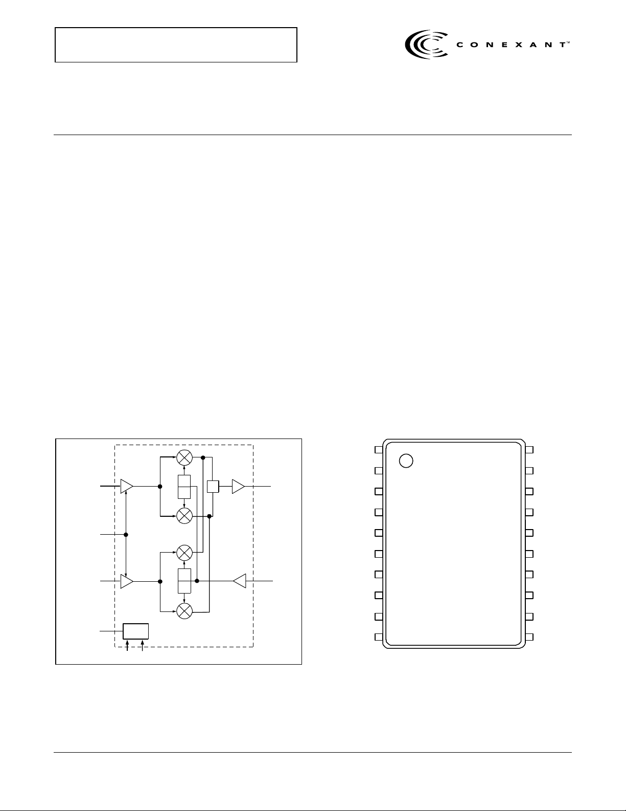
Dual-Band, Image-Reject Downconverters For GSM Applications
The RF210A and RF210B devices are available as a dual-band front end for Global
System for Mobile Communications (GSM) handset applications. Both of these
highly integrated, monolithic devices are optimized for dual-band use in
GSM900/DCS1800 or GSM 900/PCS1900 applications. The devices include two
Low Noise Amplifiers (LNAs), two image-reject mixers, and two Local Oscillator
(LO) buffer amplifiers.
The main advantage of the RF210A and RF210B is their ability to provide 30 dB of
image rejection for both the GSM900 and the DCS1800 (or PCS1900) bands
without requiring the use of a post-LNA image reject filter. A block diagram of the
RF210(A/B) is shown in Figure 1. The device package and pin configuration are
shown in Figure 2.
LNA900GND
BIASGND
LNA900IN
0
90
90
IFOUT
Features
• LNA/image-reject mixer for RF to IF conversion
• 10 dB (RF210A) or 20 dB (RF210B) switchable
gain for GSM
• 8 dB (RF210A) or 16 dB (RF210B) switchable gain
for DCS/PCS
• 30 dB of image rejection. No post-LNA filtering
required
• High isolation LO input buffer
• Differential IF output
• High dynamic range
• Three-cell battery operation (2.7 to 5 V)
• 20-pin Thin Shrink Small Outline Package
(TSSOP)
Applications
• Dual-band digital cellular mobile telephony
(GSM900/DCS 1800 or GSM900/PCS1900)
NC
1
2
3
20
19
18
MIXVCC
MIXGND
BYP900
GAINSEL
LNA1800IN
BANDSEL
Data Sheet
IRM
0
90
BIAS
BYP900
BYP1800
Figure 1. RF210(A/B) Block Diagram
Proprietary Information and Specifications are Subject to Change October 20, 1999
LOIN
C069
Conexant
LNA900IN
BIASVCC
LNAVCC
GAINSEL
LNA1800IN
LNA1800GND
ENA
4
5
6
7
8
9
10
Figure 2. RF210(A/B) Pin Configuration – 20-Pin TSSOP
IFOUT+
17
IFOUT-
16
BYP1800
15
BANDSEL
14
LOIN
13
LOGND
12
ADJMIX
11
C067
Doc. No. 100775A
Page 2
RF210(A/B) Image-Reject Downconverter
Technical Description
The RF210(A/B) dual-band, image-reject downconverters
implement the front-end functions of a dual-band superheterodyne receiver. These devices consist of two receive
paths, one for GSM900 and the other for DCS1800 (or
PCS1900). Each receive path contains an LNA and an imagereject mixer. The IF and LO ports are common to both receive
paths. The image-reject mixers can provide 30 dB of image
rejection for both the GSM900 and the DCS1800 (or PCS1900)
bands without using any post-LNA image reject filters.
The LNA/mixer combination has a switchable gain. The RF210A
and RF210B both have 22 dB of gain in the high gain mode. For
the RF210A, the gain is reduced by 10 dB (GSM band) and by
8 dB (DCS/PCS band) in the low gain mode. For the RF210B,
the gain is reduced by 20 dB (GSM band) and by 16 dB
(DCS/PCS band) in the low gain mode. The gain mode is
selected using the GAINSEL pin (Pin 7). Low gain mode is
selected by driving the GAINSEL signal high; high gain mode is
selected by driving the signal low. In addition, small adjustments
Table 1. RF210(A/B) Signal Description
of the mixer gain can be accomplished by varying the quiescent
current on the ADJMIX pin (Pin 11). This pin can be connected
to VCC or ground through resistors. The current will increase if
the pin is connected to GND and decrease if connected to VCC.
For optimal performance, this pin should be left unconnected.
The band of operation for RF210(A/B) is selected by the
BANDSEL signal on Pin 14. It switches the receive path
between GSM900 and DCS1800 (or PCS1900) bands.
The device can operate from a three-cell battery pack (2.7 V to
5.0 V). Standby mode current is extremely low at 20 µA, which
maximizes handset standby time.
The signal pin assignments and functional pin descriptions are
found in Table 1. The absolute maximum ratings of the
RF210(A/B) are provided in Table 2, the operating conditions
are specified in Table 3, and electrical specifications are
provided in Table 4. Figure 3 shows the diagram for a typical
application circuit using the RF210(A/B) downconverter. Figure
4 provides the package dimensions for the 20-pin TSSOP
device and Figure 5 provides the tape and reel dimensions.
Pin # Name Description Pin # Name Description
1 NC No connect 11 ADJMIX Mixer bias adjust pin
2 LNA900GND 900 MHz LNA ground 12 LOGND LO input ground
3 BIASGND Bias ground 13 LOIN LO input
4 LNA900IN 900 MHz LNA input 14 BANDSEL Band selection pin
5 BIASVCC Bias supply 15 BYP1800 Bypass capacitor for 1800 MHz band
6 LNAVCC LNA supply 16 IFOUT– Mixer output (negative)
7 GAINSEL LNA gain select 17 IFOUT+ Mixer output (positive)
8 LNA1800IN 1800 MHz LNA input 18 BYP900 Bypass capacitor for 900 MHz band
9 LNA1800GND 1800 MHz LNA ground 19 MIXGND Mixer ground
10 ENA Device enable (active high) 20 MIXVCC Mixer supply
Table 2. Absolute Maximum Ratings
Parameter Minimum Maximum Units
Storage Temperature –40 +125 °C
LNA Input Power +5 dBm
Supply Voltage (VCC) –0.3 +6 V
Input Voltage Range –0.3 Vcc V
2
October 20, 1999 Proprietary Information and Specifications are Subject to Change
Conexant
100775A
Page 3
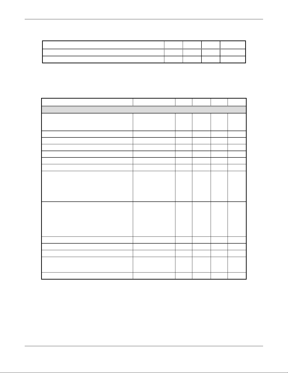
Image-Reject Downconverter RF210(A/B)
Table 3. RF210(A/B) Recommended Operating Conditions
Parameter Min Typical Max Units
Supply Voltage 2.7 3.0 5.0 V
Operating Temperature –30 +25 +85
°
C
Table 4. RF210(A/B) Electrical Specifications (1 of 2)
A
(T
= 25 C, Vcc = 3.0 V,
IF
f
= 400 MHz,
Plo
= –10 dBm)
Parameter Test Condition Min Typical Max Units
GSM900 Mode, BANDSEL = 0
Supply current:
Enable mode
Sleep mode
RF Input frequency 935 960 MHz
IF frequency 350 400 450 MHz
LO frequency 1285 1410 MHz
LO input power –10 dBm
LO to RF input isolation 30 dB
Input impedance LNA900IN = 950 MHz 40 – j50
Gain:
High gain (RF210A and RF210B)
Low gain (10 dB attenuation, RF210A)
Low gain (20 dB attenuation, RF210B)
Gain variation vs. Frequency
Gain step tracking error
Noise figure:
High gain
Low gain (12 dB gain, RF210A)
Low gain (2 dB gain, RF210B)
High gain (Note 1)
Input 1 dB compression point –25 dBm
Input third order i ntercept point –17 dBm
IF shunt resis tance/side 400 500 600
Spurious response:
2(RF) x 2(LO) and 3(RF) x 3(LO)
(Note 2):
Image rejection 35 dB
ENA = 1
ENA = 0
GAINSEL = 0
GAINSEL = 1
GAINSEL = 1
No blocker,
GAINSEL = 0
GAINSEL = 1
GAINSEL = 1
–28 dBm blocker @ 915
MHz, GAINSEL = 0
Interferer input = –75 dBm –45 dB
38
22
12
2
0.5 1
3.3
9.0
17
3.9
10
0.5
3.9
11
19
mA
µ
dB
dB
dB
dB
dB
dB
dB
dB
dB
Ω
Ω
A
100775A
Conexant
Proprietary Information and Specifications are Subject to Change October 20, 1999
3
Page 4

RF210(A/B) Image-Reject Downconverter
Table 4. RF210(A/B) Electrical Specifications (2 of 2)
A
(T
= 25 C, Vcc = 3.0 V,
IF
f
= 400 MHz,
Plo
= –10 dBm)
Parameter Test Condition Min Typical Max Units
DCS1800/PCS1900 Mode, BANDSEL = 1
Supply current:
Enable mode
Sleep mode
RF input frequency 1805 1990 MHz
IF frequency 350 400 450 MHz
LO frequency 1355 1640 MHz
LO to RF input isolation 30 dB
Input impedance LNA1800IN = 1900 MHz 40 – j10
Gain:
High gain (RF210A and RF210B)
Low gain (8 dB attenuation, RF210A)
Low gain (16 dB attenuation, RF210B)
Gain variation vs. Frequency
Gain step tracking error
Noise figure:
High gain (19 dB gain, RF210A and RF210B)
Low gain (11 dB gain, RF210A)
Low gain (3 dB gain, RF210B)
High gain (19 dB gain, RF210A and RF210B)
(Note 3)
Input 1 dB compression point –24 dBm
Input third order i ntercept point –17 dBm
IF shunt resis tance/side 400 500 600
Spurious response (N ote 2):
2(RF) x 2(LO) and 3(RF) x 3(LO)
Image rejection 35 dB
Enable (ENA) and gain select (GAINSEL) input voltages:
IH
V
IL
V
Enable (ENA) and gain select (GAINSEL) input currents:
IH
I
IL
I
Enable time 15
Bandselect switching time 15
Note 1
: Assumes 0 dBm @ 915 MHz bloc ker at the antenna input att enuated by 28 dB.
Note 2
: The rejection is specified with r espect to the desired signal gain.
Note 3
: Assumes –12 dBm @ 1785 MHz bloc ker at the antenna input att enuated by 10 dB.
ENA = 1
ENA = 0
GAINSEL = 0
GAINSEL = 1
GAINSEL = 1
No blocker,
GAINSEL = 0
GAINSEL = 1
GAINSEL = 1
–22 dBm blocker,
GAINSEL = 0
Interferer = –65 dBm
Control Signals (All Modes)
1.9
–10
42
19
11
3
0.5 1
3.5
9.0
15
4.1
250
0.5
4.5
11
16
mA
µ
dB
dB
dB
dB
dB
dB
dB
dB
dB
–53 dB
0.8
20
–1
100
0
µ
µ
µ
µ
Ω
Ω
V
V
A
A
A
s
s
4
Conexant
October 20, 1999 Proprietary Information and Specifications are Subject to Change
100775A
Page 5

Image-Reject Downconverter RF210(A/B)
VCC
RFCRFCRFC
.01 µF
RF210
100 pF
IFOUT+
IFOUT-
22 pF
82 nH82 nH
2.2
pF
68 nH
68 nH
400 MHz SAW Filter
Siemens
(B4806)
56 nH
68 nH
68 nH
100 nH
100 nH
150 pF
IF XCVR
150 pF
B4806
7
Coil
1
6
IN2
OUT2
2
5
IN1
OUT1
Ground
348
2.2
pF
17
16
ENABLE
900 MHz GSM
Fujitsu
FAR-F5CE-947M50-D235
FL200
5
2
In Out
Ground
1346
1.5 pF
6.8 nH
22 pF
10
ENA
LNA900IN
4
.01 µF
22 pF
.01 µF
22 pF
2056
0
90
90
Gain Select
1800 MHz DCS
Band Select
Fujitsu
FAR-F6CE-1G8425-L2YB
FL201
5
2
In Out
Ground
1346
2K
2K
1.5 pF
22 pF
1.5 nH
22 pF
22 pF
GAINSEL
7
8
LNA1800IN
BANDSEL
14
IRM
0
90
BIAS
BYP900
2.2 nF
BYP1800
18 15 2 3 9 12 19
2.2 nF
Ground
Figure 3. Typical RF210(A/B) Application Circuit
LOIN
ADJMIX
13
11
1
NC
LO
C070
100775A
Conexant
Proprietary Information and Specifications are Subject to Change October 20, 1999
5
Page 6

RF210(A/B) Image-Reject Downconverter
0.65 mm
1.00 mm Ref
TOP VIEW
4.40±0.10 mm
Pin #1 indicator
6.40 mm
BOTTOM VIEW
6.50±0.10 mm
0.24+0.06/-0.05 mm
1.00+0.5/-0.2 mm
1.20 mm max
0.10±0.05 mm
Pin #1
indicator
1.20
END VIEW
8.00 ± 0.10
4.00
6.75 ± 0.10
SIDE VIEW
Figure 4. RF210(A/B) Package Dimensions – 20-Pin TSSOP
4.00 ± 0.10
8
1.50 ± 0.10
0.292 ± 0.013
o
Max 7o Max
1.70 ± 0.10
2.00 ± 0.05
1.50 ± 0.25
7.05 ± 0.10
Figure 5. RF210(A/B) Tape and Reel Dimensions
1.75 ± 0.10
5.50 ± 0.05
12.00 +0.30/-0.10
Notes:
1. Carrier tape material: black conductive polycarbonate
2. Cover tape material: transparent conductive PSA
3. Cover tape size: 9.3 mm width
4. Tolerance: .XX = ±0.10
5. Quantity: 2500 per reel
6. All measurements are in millimeters
C003
C879
6
Conexant
October 20, 1999 Proprietary Information and Specifications are Subject to Change
100775A
Page 7

Image-Reject Downconverter RF210(A/B)
Ordering Information
Model Name Ma nufacturing Part
Dual-Band, Image-Reject Downconverter:
10 dB switchable gain
20 dB switchable gain
Product Revision
Number
RF210A
RF210B
© 2000, Conexant Syst ems, Inc. All Right s Reserved.
Information in thi s document is provided in connection with Conexant Systems, Inc . ("Conexant") products. These materials are provided by Conexant as a service to its
customers and may be used for informational purposes only. Conexant assumes no respons ibility for errors or omissions in these mater ials. Conexant may make changes to
specifications and product descr iptions at any time, without notice. Conexant makes no commitment to updat e the information and shall have no responsibility whatsoever
for conflicts or incompat ibilities arising from future changes t o it s specifications and product descriptions.
No license, express or implied, by estoppel or otherwise, to any intellect ual property rights is granted by this document. Except as provided in Conexant’s Terms and
Conditions of Sale for such pr oducts, Conexant assumes no liability whatsoever.
THESE MATERIALS ARE PROVIDED "AS IS" WITHOUT WARRANTY OF ANY KIND, EITHER EXPRESS OR IMPLI ED, RELATING TO SALE AND/OR USE OF
CONEXANT PRODUCTS INCLUDING LIABILITY OR WARRANTIES RELATING TO FITNESS FOR A PARTI CULAR PURPOSE, CONSEQUENTIAL OR INCIDENTAL
DAMAGES, MERCHANTABILITY, OR INFRINGEMENT OF ANY PATENT, COPYRIGHT OR OTHER INTELLECTUAL PROPERTY RIGHT. CONEXANT FURTHER
DOES NOT WARRANT THE ACCURACY OR COMPLETENESS OF THE INFORMATION, TEXT, GRAPHICS OR OTHER ITEMS CONTAINED WITHI N THESE
MATERIALS. CONEXANT SHALL NOT BE LIABLE FOR ANY SPECIAL, INDIRECT, I NCIDENTAL, OR CONSEQUENTIAL DAMAGES, INCLUDING WITHOUT
LIMITATION, LOST REVENUES OR LOST PROFITS, WHICH MAY RESULT FROM THE USE OF THESE MATERIALS.
Conexant products ar e not intended for use in medic al, lifesaving or life sustaini ng applications. Conexant customers usi ng or selling Conexant produc ts for use in suc h
applications do so at their own risk and agr ee to fully indemnify Conexant for any damages resulting from such improper use or sale.
The following are trademarks of Conexant Systems, Inc.: Conexant™, the Conexant C symbol , and “What’s Next in Communications Technologies”™. Product names or
services l isted in this publi cation are for identi fication purposes only, and may be trademark s of third parties. Third-party brands and names are the property of their
respective owners.
Additional information, posted at www.conex ant.com, is incorporated by reference.
Reader Response
tech.pubs@conexant .com. For technical questions, contact your local Conex ant sales office or field applications engineer.
100775A
: Conexant strives to produce quality documentation and welcomes your feedback. Pleas e send comments and suggestions to
Conexant
Proprietary Information and Specifications are Subject to Change October 20, 1999
7
Page 8

Further Information:
literature@conexant.com
1-800-854-8099 (North America)
33-14-906-3980 (International)
Web Site
www.conexant.com
Hong Kong
Phone: (852) 2 827 0181
Fax: (852) 2 827 6488
India
Phone: (91 11) 692 4780
Fax: (91 11) 692 4712
World Headquarters
Conexant Systems, Inc.
4311 Jamboree Road,
P.O. Box C
Newport Beach, CA 92658-8902
Phone: (949) 483-4600
Fax: (949) 483-6375
U.S. Florida/So uth Ameri ca
Phone: (727) 799-8406
Fax: (727) 799-8306
U.S. Los Angeles
Phone: (805) 376-0559
Fax: (805) 376-8180
U.S. Mid-Atlantic
Phone: (215) 244-6784
Fax: (215) 244-9292
U.S. North Central
Phone: (630) 773-3454
Fax: (630) 773-3907
U.S. Northeast
Phone: (978) 367-3200
Fax: (978) 256-6868
U.S. Northwest/Pacific West
Phone: (408) 249-9696
Fax: (408) 249-7113
U.S. South Central
Phone: (972) 733-0723
Fax: (972) 407-0639
U.S. Southeast
Phone: (919) 858-9110
Fax: (919) 858-8669
U.S. Southwest
Phone: (949) 483-9119
Fax: (949) 483-9090
APAC Headquarters
Conexant Systems Singapore,
Pte. Ltd.
1 Kim Seng Promenade
Great World City
#09-01 East Tower
Singapore 237994
Phone: (65) 737 7355
Fax: (65) 737 9077
Australia
Phone: (61 2) 9869 4088
Fax: (61 2) 9869 4077
China
Phone: (86 2) 6361 2515
Fax: (86 2) 6361 2516
Korea - Seoul Office
Phone: (82 2) 565 2880
Fax: (82 2) 565 1440
Korea - Taegu Office
Phone: (82 53) 745 2880
Fax: (82 53) 745 1440
Europe Headquarters
Conexant Systems France
Les Taissounieres B1
1681 Route des Dolines
BP 283
06905 Sophia Antipolis Cedex
France
Phone: (33 1) 41 44 36 50
Fax: (33 1) 93 00 33 03
Europe Central
Phone: (49 89) 829 1320
Fax: (49 89) 834 2734
Europe Mediterranean
Phone: (39 02) 9317 9911
Fax (39 02) 9317 9913
Europe North
Phone: (44 1344) 486 444
Fax: (44 1344) 486 555
Europe South
Phone: (33 1) 41 44 36 50
Fax: (33 1) 41 44 36 90
Middle East Headquarters
Conexant Systems Commercial
(Israel) Ltd.
P.O. Box 12660
Herzlia 46733
Israel
Phone: (972 9) 952 4064
Fax: (972 9) 951 3924
Japan Headquarters
Conexant Systems Japan Co., Ltd.
Shimomoto Bui lding
1-46-3 Hatsudai,
Shibuya-ku
Tokyo, 151-0061
Japan
Phone: (81 3) 5371 1567
Fax: (81 3) 5371 1501
Taiwan Headquar ters
Conexant Systems, Taiwan Co.,
Ltd.
Room 2808
International Trade Building
333 Keelung Road, Section 1
Taipei 110
Taiwan, ROC
Phone: (886 2) 2720 0282
Fax: (886 2) 2757 6760
 Loading...