

Page 1
©
1989 Burr-Brown Corporation PDS-900E Printed in U.S.A. October, 1993
DESCRIPTION
The REF102 is a precision 10V voltage reference. The
drift is laser-trimmed to 2.5ppm/°C max (CM grade)
over the industrial temperature range and 5ppm/°C
max (SM grade) over the military temperature range.
The REF102 achieves its precision without a heater.
This results in low power, fast warm-up, excellent
stability, and low noise. The output voltage is extremely insensitive to both line and load variations and
can be externally adjusted with minimal effect on drift
and stability. Single supply operation from 11.4V to
36V and excellent overall specifications make the
REF102 an ideal choice for demanding instrumentation and system reference applications.
APPLICATIONS
● PRECISION-CALIBRATED VOLTAGE
STANDARD
● D/A AND A/D CONVERTER REFERENCE
● PRECISION CURRENT REFERENCE
● ACCURATE COMPARATOR THRESHOLD
REFERENCE
● DIGITAL VOLTMETERS
● TEST EQUIPMENT
● PC-BASED INSTRUMENTATION
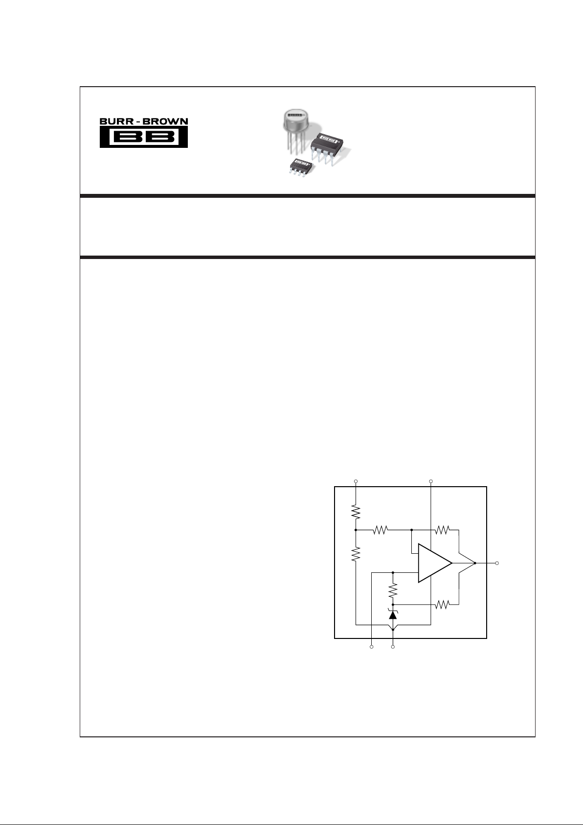
REF102
–
+
A
R
2
R
3
R
4
R
6
R
1
R
5
1
50k Ω
22k Ω
7k Ω
4k Ω
8k Ω
DZ
1
Noise
Reduction
Common
V
OUT
V+
Trim
14k Ω
52
6
84
Precision
VOLTAGE REFERENCE
FEATURES
● +10V ±0.0025V OUTPUT
● VERY LOW DRIFT: 2.5ppm/
°C max
● EXCELLENT STABILITY:
5ppm/1000hr typ
● EXCELLENT LINE REGULATION:
1ppm/V max
● EXCELLENT LOAD REGULATION:
10ppm/mA max
● LOW NOISE: 5
µVp-p typ, 0.1Hz to 10Hz
● WIDE SUPPLY RANGE: 11.4VDC to 36VDC
● LOW QUIESCENT CURRENT: 1.4mA max
● PACKAGE OPTIONS: HERMETIC TO-99,
PLASTIC DIP, SOIC
®
International Airport Industrial Park • Mailing Address: PO Box 11400, Tucson, AZ 85734 • Street Address: 6730 S. Tucson Blvd., Tucson, AZ 85706 • Tel: (520) 746-1111 • Twx: 910-952-1111
Internet: http://www.burr-brown.com/ • FAXLine: (800) 548-6133 (US/Canada Only) • Cable: BBRCORP • Telex: 066-6491 • FAX: (520) 889-1510 • Immediate Product Info: (800) 548-6132
REF102
REF102
Page 2
®
REF102
2
The information provided herein is believed to be reliable; however, BURR-BROWN assumes no responsibility for inaccuracies or omissions. BURR-BROWN assumes
no responsibility for the use of this information, and all use of such information shall be entirely at the user’s own risk. Prices and specifications are subject to change
without notice. No patent rights or licenses to any of the circuits described herein are implied or granted to any third party. BURR-BROWN does not authorize or warrant
any BURR-BROWN product for use in life support devices and/or systems.
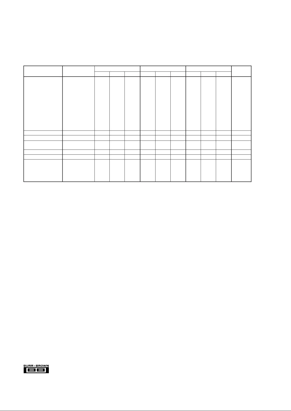
SPECIFICATIONS
ELECTRICAL
At TA = +25°C and VS = +15V power supply, unless otherwise noted.
REF102A, R REF102B, S REF102C, M
PARAMETER CONDITIONS MIN TYP MAX MIN TYP MAX MIN TYP MAX UNITS
OUTPUT VOLTAGE
Initial T
A
= 25°C 9.99 10.01 9.995 10.005 9.9975 10.0025 V
vs Temperature
(1)
10 5 2.5 ppm/°C
vs Supply
(Line Regulation) V
S
= 11.4V to 36V 2 1 1 ppm/V
vs Output Current
(Load Regulation) I
L
= 0mA to +10mA 20 10 10 ppm/mA
I
L
= 0mA to –5mA 40 20 20 ppm/mA
vs Time T
A
= 25°
M Package 5 ✻✻ppm/1000hr
P, U Packages
(2)
20 ✻ ppm/1000hr
Trim Range
(3)
±3 ✻✻ %
Capacitive Load, max 1000 ✻✻pF
NOISE (0.1Hz to 10Hz) 5 ✻✻µVp-p
OUTPUT CURRENT +10, –5 ✻✻ mA
INPUT VOLTAGE
RANGE +11.4 +36 ✻✻✻ ✻V
QUIESCENT CURRENT (I
OUT
= 0) +1.4 ✻✻mA
WARM-UP TIME
(4)
(To 0.1%) 15 ✻✻µs
TEMPERATURE
RANGE
Specification
REF102A, B, C –25 +85 ✻✻✻ ✻°C
REF102R, S –55 +125 ✻✻ °C
✻ Specifications same as REF102A/R.
NOTES: (1) The “box” method is used to specify output voltage drift vs temperature. See the Discussion of Performance section. (2) Typically 5ppm/1000hrs after 168hr
powered stabilization. (3) Trimming the offset voltage affects drift slightly. See Installation and Operating Instructions for details. (4) With noise reduction pin floating.
See Typical Performance Curves for details.
Page 3

REF102
®
3
TEMPERATURE MAX INITIAL MAX DRIFT
PRODUCT PACKAGE RANGE ERROR (mV) (ppm/
°C)
REF102AU 8-Pin SOIC –25°C to +85°C ±10 ±10
REF102AP 8-Pin Plastic DIP –25°C to +85°C ±10 ±10
REF102BP 8-Pin Plastic DIP –25°C to +85°C ±5 ±5
REF102AM Metal TO-99 –25°C to +85°C ±10 ±10
REF102BM Metal TO-99 –25°C to +85°C ±5 ±5
REF102CM Metal TO-99 –25°C to +85°C ±2.5 ±2.5
REF102RM Metal TO-99 –55°C to +125°C ±10 ±10
REF102SM Metal TO-99 –55°C to +125°C ±5 ±5
ORDERING INFORMATION
PIN CONFIGURATIONS
Top View DIP/SOIC
8
71
4
53
26
Common
Trim
V
OUT
NCNC
NC
Noise Reduction
8
7
6
5
1
2
3
4
Noise Reduction
NC
V
OUT
Trim
NC
V+
Com
NC
V+
Top View TO-99
Input Voltage...................................................................................... +40V
Operating Temperature
P,U ..................................................................................–25°C to +85°C
M ................................................................................... –55°C to +125°C
Storage Temperature Range
P,U ..................................................................................–40°C to +85°C
M ................................................................................... –65°C to +150°C
Lead Temperature (soldering, 10s)................................................ +300°C
(SOIC, 3s) ....................................................... +260°C
Short-Circuit Protection to Common or V+............................... Continuous
ABSOLUTE MAXIMUM RATINGS
PACKAGE INFORMATION
PACKAGE DRAWING
PRODUCT PACKAGE NUMBER
(1)
REF102AU 8-Pin SOIC 182
REF102AP 8-Pin Plastic DIP 006
REF102BP 8-Pin Plastic DIP 006
REF102AM Metal-TO-99 001
REF102BM Metal-TO-99 001
REF102CM Metal-TO-99 001
REF102RM Metal-TO-99 001
REF102SM Metal-TO-99 001
NOTE: (1) For detailed drawing and dimension table, please see end of data
sheet, or Appendix C of Burr-Brown IC Data Book.
ELECTROSTATIC
DISCHARGE SENSITIVITY
This integrated circuit can be damaged by ESD. Burr-Brown
recommends that all integrated circuits be handled with
appropriate precautions. Failure to observe proper handling
and installation procedures can cause damage.
ESD damage can range from subtle performance degradation
to complete device failure. Precision integrated circuits may
be more susceptible to damage because very small parametric
changes could cause the device not to meet its published
specifications.
Page 4

®
REF102
4
TYPICAL PERFORMANCE CURVES
At TA = +25°C, VS = +15V, unless otherwise noted.
FPO
V
IN
V
OUT
Time (10ms/div)
Power Turn-On
FPO
POWER TURN-ON RESPONSE with 1µF Cn
FPO
V
IN
POWER TURN-ON RESPONSE
V
OUT
Time (5µs/div)
Power Turn-On
LOAD REGULATION
+1.5
+1.0
+0.5
0
–0.5
–1.0
–1.5
–5 0 +5 +10
Output Current (mA)
Output Voltage Change (mV)
POWER SUPPLY REJECTION vs FREQUENCY
130
120
110
100
90
80
70
60
1 100 1k 10k
Frequency (Hz)
Power Supply Rejection (dB)
QUIESCENT CURRENT vs TEMPERATURE
1.6
1.4
1.2
1.0
0.8
–50 –25 0 +25 +50 +75 +100 +125
Temperature (°C)
Quiescent Current (mA)
–75
RESPONSE TO THERMAL SHOCK
30 45 60150
+600
+300
0
–300
–600
T
A
=
+25°C
REF102CM Immersed in +85°C Fluorinert Bath
Output Voltage Change (µV)
Time (s)
TA = +85°C
Page 5

REF102
®
5
TYPICAL PERFORMANCE CURVES (CONT)
At TA = +25°C, VS = +15V, unless otherwise noted.
Low Frequency Noise (1s /div)
(See Noise Test Circuit)
6
4
2
0
–2
–4
–6
TYPICAL REF102 REFERENCE NOISE
F P O
Noise Test Circuit.
–
+
OPA27
DUT
100µF
15.8kΩ
20Ω 2kΩ
8KΩ
2µF
Oscilloscope
Gain = 100V/V
f = 0.1Hz and 10Hz
–3dB
Noise Voltage (µV)
Page 6

®
REF102
6
THEORY OF OPERATION
Refer to the diagram on the first page of this data sheet. The
10V output is derived from a compensated buried zener
diode DZ1, op amp A1, and resistor network R1–R6.
Approximately 8.2V is applied to the non-inverting input of
A
1
by DZ1. R1, R2, and R3 are laser-trimmed to produce an
exact 10V output. The zener bias current is established from
the regulated output voltage through R4. R5 allows usertrimming of the output voltage by providing for small
external adjustment of the amplifier gain. Because the TCR
of R
5
closely matches the TCR of R1, R2 and R3 , the voltage
trim has minimal effect on the reference drift. The output
voltage noise of the REF102 is dominated by the noise of the
zener diode. A capacitor can be connected between the
Noise Reduction pin and ground to form a low-pass filter
with R
6
and roll off the high-frequency noise of the zener.
DISCUSSION
OF PERFORMANCE
The REF102 is designed for applications requiring a precision voltage reference where both the initial value at room
temperature and the drift over temperature are of importance
to the user. Two basic methods of specifying voltage reference drift versus temperature are in common usage in the
industry—the “butterfly method” and the “box method.”
The REF102 is specified with the more commonly used
“box method.” The “box” is formed by the high and low
specification temperatures and a diagonal, the slope of
which is equal to the maximum specified drift.
Since the shape of the actual drift curve is not known, the
vertical position of the box is not exactly known either. It is,
however, bounded by V
UPPER BOUND
and V
LOWER BOUND
(see
Figure 1). Figure 1 uses the REF102CM as an example. It
has a drift specification of 2.5ppm/°C maximum and a
specification temperature range of –25°C to +85°C. The
“box” height, V1 to V2, is 2.75mV.
FIGURE 1. REF102CM Output Voltage Drift.
2.75mV
Worst-case
∆V
OUT
for
REF102CM
INSTALLATION AND
OPERATING INSTRUCTIONS
BASIC CIRCUIT CONNECTION
Figure 2 shows the proper connection of the REF102. To
achieve the specified performance, pay careful attention to
layout. A low resistance star configuration will reduce voltage errors, noise pickup, and noise coupled from the power
supply. Commons should be connected as indicated being
sure to minimize interconnection resistances.
Minimum range (±300mV) and minimal
degradation of drift.
FIGURE 3. REF102 Optional Output Voltage Adjust.
NOTES: (1) Lead resistances here of up to a few ohms have negligible
effect on performance. (2) A resistance of 0.1Ω in series with these
leads will cause a 1mV error when the load current is at its maximum of
10mA. This results in a 0.01% error of 10V.
FIGURE 2. REF102 Installation.
OPTIONAL OUTPUT VOLTAGE ADJUSTMENT
Optional output voltage adjustment circuits are shown in
Figures 3 and 4. Trimming the output voltage will change
the voltage drift by approximately 0.008ppm/°C per mV of
trimmed voltage. In the circuit in Figure 3, any mismatch in
TCR between the two sections of the potentiometer will also
affect drift, but the effect of the ∆TCR is reduced by a factor
of five by the internal resistor divider. A high quality
potentiometer, with good mechanical stability, such as a
cermet, should be used. The circuit in Figure 3 has a
minimum trim range of ±300mV. The circuit in Figure 4 has
less range but provides higher resolution. The mismatch in
TCR between R
S
and the internal resistors can introduce
some slight drift. This effect is minimized if R
S
is kept
significantly larger than the 50kΩ internal resistor. A TCR
of 100ppm/°C is normally sufficient.
REF102BM V
UPPER BOUND
+10.00275
V
1
V
NOMINAL
+10.0000
V
2
+9.99725
REF102BM V
LOWER BOUND
–25 0 +25 +50 +85
Output Voltage (V)
Temperature (°C)
REF102
1µF
Tantalum
+
R
L 1RL 2RL 3
V+
(1)
2
(2)
(2)
(1)
4
6
REF102
1µF
Tantalum
+
V+
2
4
20k
Output
Voltage
Adjust
Ω
+10V
5
V
TRIM
6
V
OUT
Page 7

REF102
®
7
FIGURE 4. REF102 Optional Output Voltage Fine Adjust.
Higher resolution, reduced range (typically ±25mV).
APPLICATIONS INFORMATION
High accuracy, extremely low drift, outstanding stability,
and low cost make the REF102 an ideal choice for all
instrumentation and system reference applications. Figures 6
through 14 show a variety of useful application circuits.
FIGURE 6. –10V Reference Using a) Resistor or b) OPA27.
See AB-004 for more detail
1.4mA < (5V –I
L
) < 5.4mA
R
S
OPTIONAL NOISE REDUCTION
The high-frequency noise of the REF102 is dominated by
the zener diode noise. This noise can be greatly reduced by
connecting a capacitor between the Noise Reduction pin and
ground. The capacitor forms a low pass filter with R
6
(refer
to the figure on the first page of the data sheet) and attenuates the high-frequency noise generated by the zener. Figure
5 shows the effect of a 1µF noise reduction capacitor on the
high frequency noise of the REF102. R6 is typically 7kΩ so
the filter has a –3dB frequency of about 22Hz. The result is
a reduction in noise from about 800µVp-p to under 200µ
Vp-p. If further noise reduction is required, use the circuit in
Figure 14.
FIGURE 5. Effect of 1µF Noise Reduction Capacitor on
Broadband Noise (f
–3dB
= 1MHz).
CN = 1µF
NO C
N
6
b) Precision –10V Reference.
a) Resister Biased –10V Reference
R
S
I
L
4
REF102
2
–10V Out
V+ (1.4V to 26V)
2
6
4
10V
OPA27
R
1
2kΩ
C
1000pF
1
–10V Out
–15V
REF102
V+ (1.4V to 26V)
REF102
V+
2
4
20k
Output
Voltage
Adjust
Ω
+10V
5
V
TRIM
6
V
OUT
R
S
1M Ω
1µF
Tantalum
+
Page 8

®
REF102
8
See AB-005 for more details.
FIGURE 9. ±10V Reference.
FIGURE 8. Strain Gauge Conditioner for 350Ω Bridge.
I
OUT
= 10V , R ≥ 1kΩ
R
See AB-002 for more details and I Sink Circuit.
R1 = V
CC
– 10V
I
L (TYP)
a) –20mA < IL < +20mA
(OPA27 also improves transient immunity)
c) I
L (MAX)
= I
L (TYP)
+10mA
I
L (MIN)
= I
L (TYP)
–5mA
b) –5mA < I
L
< +100mA
FIGURE 7. +10V Reference With Output Current Boosted to: a) ±20mA, b) +100mA, and c) I
L (TYP)
+10mA, –5A.
Ω
–
+
OPA27
6
220
+10V
I
L
6
+10V
I
L
2N2905
6
+10V
I
L
4
REF102
V+
2
4
REF102
V+
2
4
REF102
V+
2
–
+
INA101
V
x100
2
4
6
+15V
–5V
–15V
357
1/2W
Ω
2
3
OPA27
–
+
357
1/2W
Ω
28mA
28.5mA
+5V
350 Strain
Gauge Bridge
Ω
5
10
8
R
G
OUT
6
REF102
V+
REF102
6
4
2
3
1
25kΩ
25kΩ25kΩ
25kΩ
INA105
5
6
+10V
Out
–10V
Out
2
–
+
LOAD
I
OUT
Can be connected
to ground or –V .
S
V+
REF102
2
6
4
OPA111
R
FIGURE 10. Positive Precision Current Source.
Page 9

REF102
®
9
Ω
–
+
OPA27
6
2k
+10V
REF102
(2)
2
R
1k
1
4
V
OUT 2
Ω
REF
V
C
1
1µF
C
2
1µF
R
2k
2
Ω
2
3
Ω62k
REF102
(1)
2
4
V
OUT 1
Ω62k
V
OUT N
V+
REF102
(N)
2
4
V+
V+
FIGURE 11. Stacked References.
FIGURE 13. +5V and +10V Reference.
NOTES: (1) REF102s can be stacked to obtain voltages in multiples of 10V.
(2) The supply voltage should be between 10n + 1.4 and 10n + 26 where n
is the number of REF102s. (3) Output current of each REF102 must not
exceed its rated output current of +10, –5mA. This includes the current
delivered to the lower REF102.
eN = 5µVp-p (f = 0.1Hz to 1Mhz)
N
V
REF
= (VO1 + VO2 ....V
OUT N
)
N
See AB-003 for more details.
FIGURE 14. Precision Voltage Reference with Extremely
Low Noise.
+30V
6
31.4V to 56V
2
4
6
2
6
2
4
+20V
+10V
REF102
4
REF102
REF102
–
+
2
4
6
+5V
Out
INA105
2
5
1
3
6
–5V
Out
REF102
V+
–
+
2
4
6
+10V
+5V
INA105
5
1
3
6
2
REF102
V+
FIGURE 12. ±5V Reference.
 Loading...