

Page 1
®
REF02
REF02
+5V Precision
VOLTAGE REFERENCE
REF02
FEATURES
● OUTPUT VOLTAGE: +5V ±0.1% max
● EXCELLENT TEMPERATURE STABILITY:
8.5ppm/
● LOW NOISE: 10
°C max (–40°C to +85°C)
µVp-p max (0.1Hz to 10Hz)
● EXCELLENT LINE REGULATION:
0.008%/V max
● EXCELLENT LOAD REGULATION:
0.005%/mA max
● LOW SUPPLY CURRENT: 1.4mA max
● SHORT-CIRCUIT PROTECTED
● WIDE SUPPLY RANGE: 8V to 40V
● EXTENDED INDUSTRIAL TEMPERATURE
RANGE: –40
°C to +85°C
● PACKAGE OPTIONS: Plastic DIP, SOIC
APPLICATIONS
● PRECISION REGULATORS
● CONSTANT CURRENT SOURCE/SINK
● DIGITAL VOLTMETERS
● V/F CONVERTERS
● A/D AND D/A CONVERTERS
● PRECISION CALIBRATION STANDARD
● TEST EQUIPMENT
DESCRIPTION
The REF02 is a precision 5V voltage reference. The
drift is laser trimmed to 8.5ppm/°C max over the
extended industrial and military temperature range.
The REF02 provides a stable 5V output that can be
externally adjusted over a ±6% range with minimal
effect on temperature stability. REF02 operates from a
single supply with an input range of 8V to 40V with a
very low current drain of 1mA, and excellent temperature stability due to an improved design. Excellent line
and load regulation, low noise, low power, and low
cost make the REF02 the best choice whenever a 5V
voltage reference is required. All popular package
options are available: plastic DIP, and SOIC. The
REF02 is an ideal choice for portable instrumentation,
temperature transducers, A/D and D/A converters, and
digital voltmeter.
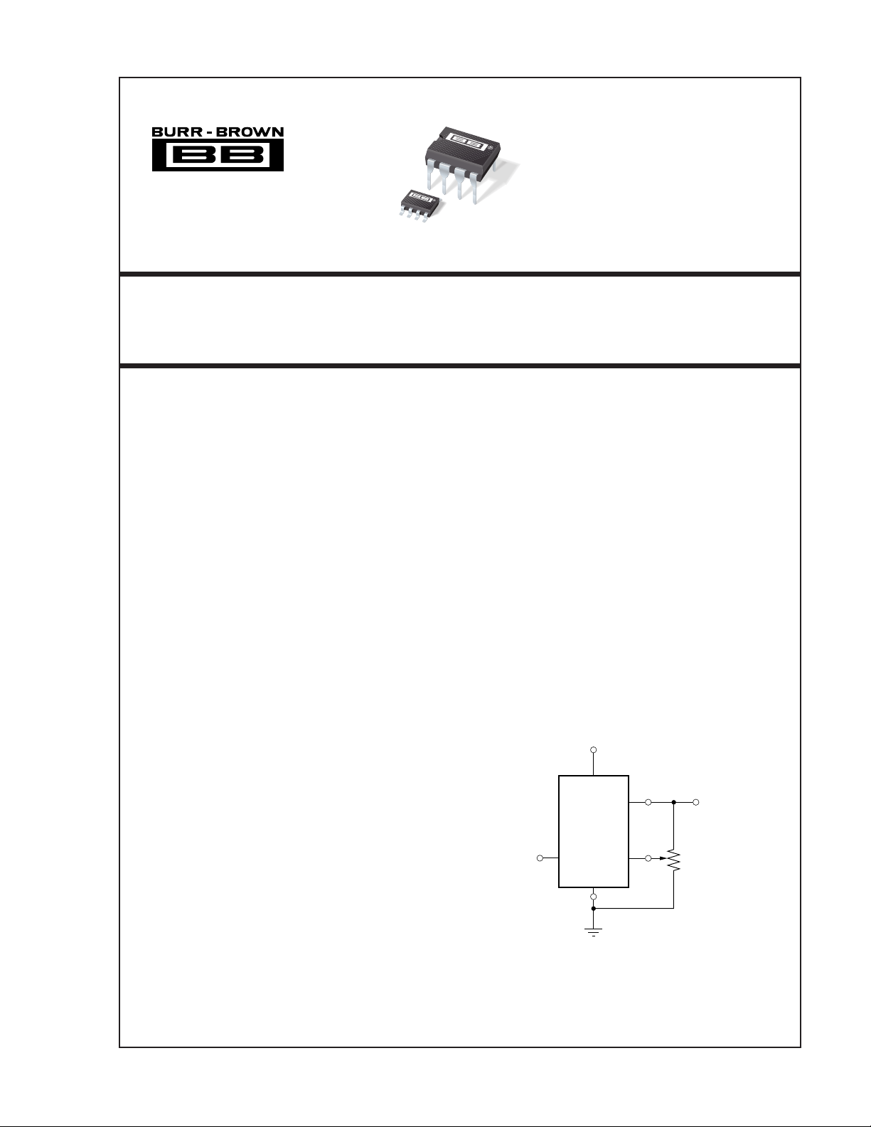
2
V
IN
6
V
OUT
REF02
3
Temp
GND
4
Trim
5
Output
R
POT
10kΩ
(Optional)
+5V Reference with Trimmed Output
International Airport Industrial Park • Mailing Address: PO Box 11400, Tucson, AZ 85734 • Street Address: 6730 S. Tucson Blvd., Tucson, AZ 85706 • Tel: (520) 746-1111 • Twx: 910-952-1111
Internet: http://www.burr-brown.com/ • FAXLine: (800) 548-6133 (US/Canada Only) • Cable: BBRCORP • Telex: 066-6491 • FAX: (520) 889-1510 • Immediate Product Info: (800) 548-6132
©
1993 Burr-Brown Corporation PDS-1177G Printed in U.S.A. December, 1993
Page 2
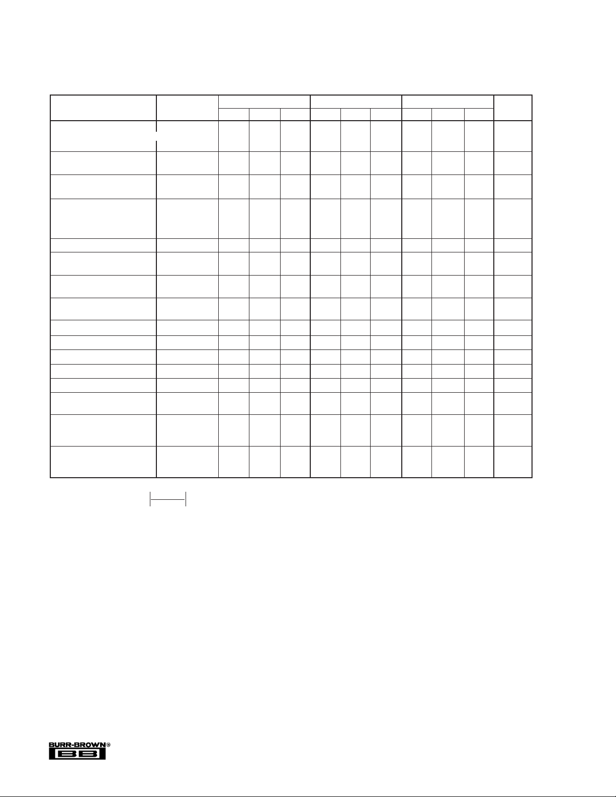
SPECIFICATIONS
ELECTRICAL
At TA = +25°C and VIN = +15V power supply, unless otherwise noted.
REF02A, R REF02B, S REF02C
PARAMETER CONDITIONS MIN TYP MAX MIN TYP MAX MIN TYP MAX UNITS
OUTPUT VOLTAGE I
Change with Temperature
(1, 2)
(∆VOT)
–40°C to +85°C 0.05 0.19 0.05 0.13 0.05 0.11 %
OUTPUT VOLTAGE DRIFT
(3)
–40°C to +85°C (TCVO) 4 15 4 10 4 8.5 ±ppm/°C
OUTPUT ADJUSTMENT
RANGE R
CHANGE IN V
COEFFICIENT WITH
TEMP
O
OUTPUT ADJUSTMENT
(–55°C to +125°C) R
OUTPUT VOLTAGE NOISE 0.1Hz to 10Hz
LINE REGULATION
(4)
–40°C to +85°CV
LOAD REGULATION
(4)
–40°C to +85°CI
TURN-ON SETTLING TIME To ±0.1% 5 ✻✻µs
QUIESCENT CURRENT No Load 1.0 1.4 ✻✻ ✻✻ mA
LOAD CURRENT (SOURCE) 10 21 ✻✻ ✻✻ mA
LOAD CURRENT (SINK) –0.3 –0.5 ✻✻ ✻✻ mA
SHORT-CIRCUIT CURRENT V
POWER DISSIPATION No Load 15 21 ✻✻ ✻✻mW
TEMPERATURE VOLTAGE
(7)
OUTPUT
TEMPERATURE COEFFICIENT
of Temperature Pin Voltage
–55°C to +125°C 2.1 mV/°C
TEMPERATURE RANGE
Specification
REF02A, B, C –40 +85 ✻✻✻✻°C
NOTES: (1) ∆VOT is defined as the absolute difference between the maximum output and the minimum output voltage over the specified temperature range expressed
as a percentage of 5V: (2) ∆V
V
∆V
= x 100
O
the temperature range. (4) Line and load regulation specifications include the effect of self heating. (5) Sample tested. (6) 10kΩ potentiometer connected between
V
and ground with wiper connected to Trim pin. See Figure on page 1. (7) Pin 3 is insensitive to capacitive loading. The temperature voltage will be modified by
OUT
7mV for each µA of loading.
= 0mA 4.985 5.0 5.015 4.990 ✻ 5.010 4.995 ✻ 5.005 V
LOAD
(6)
= 10kΩ
POT
= 10kΩ 0.7 ✻✻ppm/%
POT
±3 ±6 ✻✻ ✻✻ %
(5)
410 ✻✻ ✻✻µVp-p
VIN = 8V to 33V 0.006 0.010 ✻✻ 0.004 0.008 %/V
= 8.5V to 33V 0.008 0.012 ✻✻ 0.005 0.010
IN
IL = 0mA to +10mA 0.005 0.010 ✻ 0.008 0.003 0.005 %/mA
= 0mA to +10mA 0.007 0.012 ✻ 0.010 0.004 0.005
L
of Final Value
= 0 30 ✻✻mA
OUT
630 ✻✻mV
– V
MAX
MIN
5V
specification applies trimmed to +5.000V or untrimmed. (3) TCVO is defined as ∆VOT divided by
OT
The information provided herein is believed to be reliable; however, BURR-BROWN assumes no responsibility for inaccuracies or omissions. BURR-BROWN assumes
no responsibility for the use of this information, and all use of such information shall be entirely at the user’s own risk. Prices and specifications are subject to change
without notice. No patent rights or licenses to any of the circuits described herein are implied or granted to any third party. BURR-BROWN does not authorize or warrant
any BURR-BROWN product for use in life support devices and/or systems.
REF02
2
Page 3

ABSOLUTE MAXIMUM RATINGS PIN CONFIGURATIONS
Input Voltage ...................................................................................... +40V
Operating Temperature
G, P, U ........................................................................... –40°C to +85°C
Storage Temperature Range
G, P, U ........................................................................... –65°C to +125°
M .................................................................................... –65°C to +150°
Output Short Circuit Duration (to Ground or V
Junction Temperature ....................................................... –65°C to +150°
θ
P ......................................................................................... 120°C/W
JA
U ........................................................................................... 80°C/W
Lead Temperature (soldering, 60s) ............................................... +300°C
) ....................... Indefinite
IN
Top View DIP/SOIC
1
NC
2
V
IN
3
Temp
4
GND
ELECTROSTATIC
DISCHARGE SENSITIVITY
This integrated circuit can be damaged by ESD. Burr-Brown
recommends that all integrated circuits be handled with
appropriate precautions. Failure to observe proper handling
and installation procedures can cause damage.
ESD damage can range from subtle performance degradation
to complete device failure. Precision integrated circuits may
be more susceptible to damage because very small parametric
changes could cause the device not to meet its published
specifications.
8
NC
7
NC
6
V
OUT
5
Trim
PACKAGE INFORMATION
PRODUCT PACKAGE NUMBER
PACKAGE DRAWING
REF02AU SOIC 182
REF02BU SOIC 182
REF02AP Plastic DIP 006
REF02BP Plastic DIP 006
NOTE: (1) For detailed drawing and dimension table, please see end of data
sheet, or Appendix C of Burr-Brown IC Data Book.
(1)
ORDERING INFORMATION
PRODUCT V
REF02AU 5V±15mV ±15 –40°C to +85°C SOIC
REF02BU 5V±10mV ±10 –40°C to +85°C SOIC
REF02AP 5V±15mV ±15 –40°C to +85°C Plastic DIP
REF02BP 5V±10mV ±10 –40°C to +85°C Plastic DIP
AT 25°C (ppm/° C) TEMPERATURE PACKAGE
OUT
MAX DRIFT
3
REF02
Page 4

TYPICAL PERFORMANCE CURVES
AT TA = +25°C, unless otherwise noted.
OUTPUT WIDEBAND NOISE
1k
100
10
Output Noise (µVp-p)
vs BANDWIDTH (0.1Hz to frequency indicated)
Line Regulation (dB)
1
10 100 1k 10k 100k 1M
Frequency (Hz)
96
86
76
66
56
46
36
26
16
6
10 100 1k 10k 100k 1M
LINE REGULATION vs FREQUENCY
Frequency (Hz)
VS = 15V
= +25°C
T
A
0.0003
0.001
0.003
0.01
0.031
0.1
0.31
Line Regulation (%/V)
1.0
3.1
10.0
0.035
0.03
0.025
0.02
0.015
0.01
0.005
Percent Change in Output Voltage (%)
Line Regulation (%/V)
OUTPUT CHANGE DUE TO THERMAL SHOCK
TA =
25°C
0
–100102030405060
6
5
4
3
2
1
0
6 6.5 7 7.5 8 8.5 9 9.5 10
TA =
75°C
Device immersed
in 75°C oil bath
Time (s)
LINE REGULATION vs SUPPLY VOLTAGE
–55°C
Input Voltage (V)
VIN = 15V
125°C
85°C
25°C
MAXIMUM LOAD CURRENT vs INPUT VOLTAGE
35
30
25
20
15
10
Maximum Load Current (mA)
5
0
5 10152025
0.03
0.025
0.02
0.015
0.01
Line Regulation (%/V)
0.005
0
5
Short Circuit Protection
500mW
Maximum
Dissapation
TA = +25°C
Input Voltage (V)
LINE REGULATION vs SUPPLY VOLTAGE
TA = 25°C
10 15 20 25 30
Input Voltage (V)
REF02
4
Page 5

TYPICAL PERFORMANCE CURVES (CONT)
MAXIMUM LOAD CURRENT vs TEMPERATURE
Temperature (°C)
30
25
20
15
10
5
0
Maximum Load Current (mA)
–60 –40 –20 0 20 40 60 80 100 120 140
VIN = 15V
At TA = +25°C, unless otherwise noted.
NORMALIZED LOAD REGULATION (∆IL = 10mA)
1.6
VIN = 15V
1.5
1.4
1.3
1.2
1.1
1.0
0.9
0.8
Load Reg (T) / Load Reg (25°C)
0.7
0.6
–60
–40 –20 0 20 40 60 80 100 120 140
5.002
5.0015
5.001
5.0005
5
Volt
4.9995
4.999
4.9985
4.998
4.9975
–40 –20 0 20 40 60 80 100 120 140
–60
vs TEMPERATURE
Temperature (°C)
REF02 V
OUT
Temperature
NORMALIZED LINE REGULATION vs TEMPERATURE
1.4
1.3
1.2
1.1
1.0
0.9
0.8
0.7
0.6
Line Reg (T) / Line Reg (25°C)
0.5
0.4
–60
–40 –20 0 20 40 60 80 100 120 140
Temperature (°C)
1.1
1.08
1.06
1.04
1.02
Quiescent Current (mA)
1.0
0.98
QUIESCENT CURRENT vs TEMPERATURE
VIN = 15V
–60 –40 –20 0 20 40 60 80 100 120 140
Temperature (°C)
TYPICAL TEMPERATURE VOLTAGE OUTPUT
830
780
730
680
VIN = 15V
630
580
530
480
Temperature Voltage Output (mV)
430
–60 –40 –20 0 20 40 60 80 100 120 140
5
vs TEMPERATURE (REF02M)
Temperature (°C)
REF02
Page 6

OUTPUT ADJUSTMENT
The REF02 trim terminal can be used to adjust the voltage
over a 5V ±150mV range. This feature allows the system
designer to trim system errors by setting the reference to a
(1)
voltage other than 5V, including 5.12V
for binary applica-
tions (see circuit on page one).
Adjustment of the output does not significantly affect the
temperature performance of the device. The temperature
coefficient change is approximately 0.7ppm/°C for 100mV of
output adjustment.
NOTE: (1) 20mV LSB for 8-bit applications.
+18V
2
V
IN
TYPICAL APPLICATIONS
2
V
IN
6
V
O
0.1µF
REF02
35
Temp
GND
4
Trim
5kΩ
10kΩ
10kΩ
+15V
OPA177
–5V
–5V
REF02
GND
4
–18V
FIGURE 1. Burn-In Circuit.
REFERENCE STACKING
PROVIDES OUTSTANDING LINE REGULATION
By stacking two REF01s and one REF02, a systems designer
can achieve 5V, 15V and 25V outputs. One very important
advantage of this circuit is the near perfect line regulation at
5V and 15V outputs. This circuit can accept a 27V to 55V
change to the input with less than the noise voltage as a
change to the output voltage. (R
supplies current (I
) for the 15V regulator.
SY
), a load bypass resistor,
B
Any number of REF01s and REF02s can be stacked in this
configuration. If ten devices can be stacked in this configuration, for example, ten 5V or five 10V outputs are achieved.
The line voltage may range from 100V to 130V. Care should
be exercised to insure that the total load currents do not
exceed the maximum usable current which is typically
21mA.
–15V
FIGURE 2. ±5V Precision Reference.
REF02
6
 Loading...