

Page 1
RD7
®
TOPSwitch-II
PC Standby Reference Design Board
90 to 375 VDC Input, 3.5 W Output
Product Highlights
Low Cost Production Worthy Reference Design
• Up to 3.5 W of output power
• Meets Blue Angel requirements (5 W)
• Single sided board
• Low cost through-hole components
• Fully assembled and tested
• Easy to evaluate and modify
• Extensive performance data
• Light weight - no heat sink required for TOPSwitch-II
• Non-isolated +12 V output option
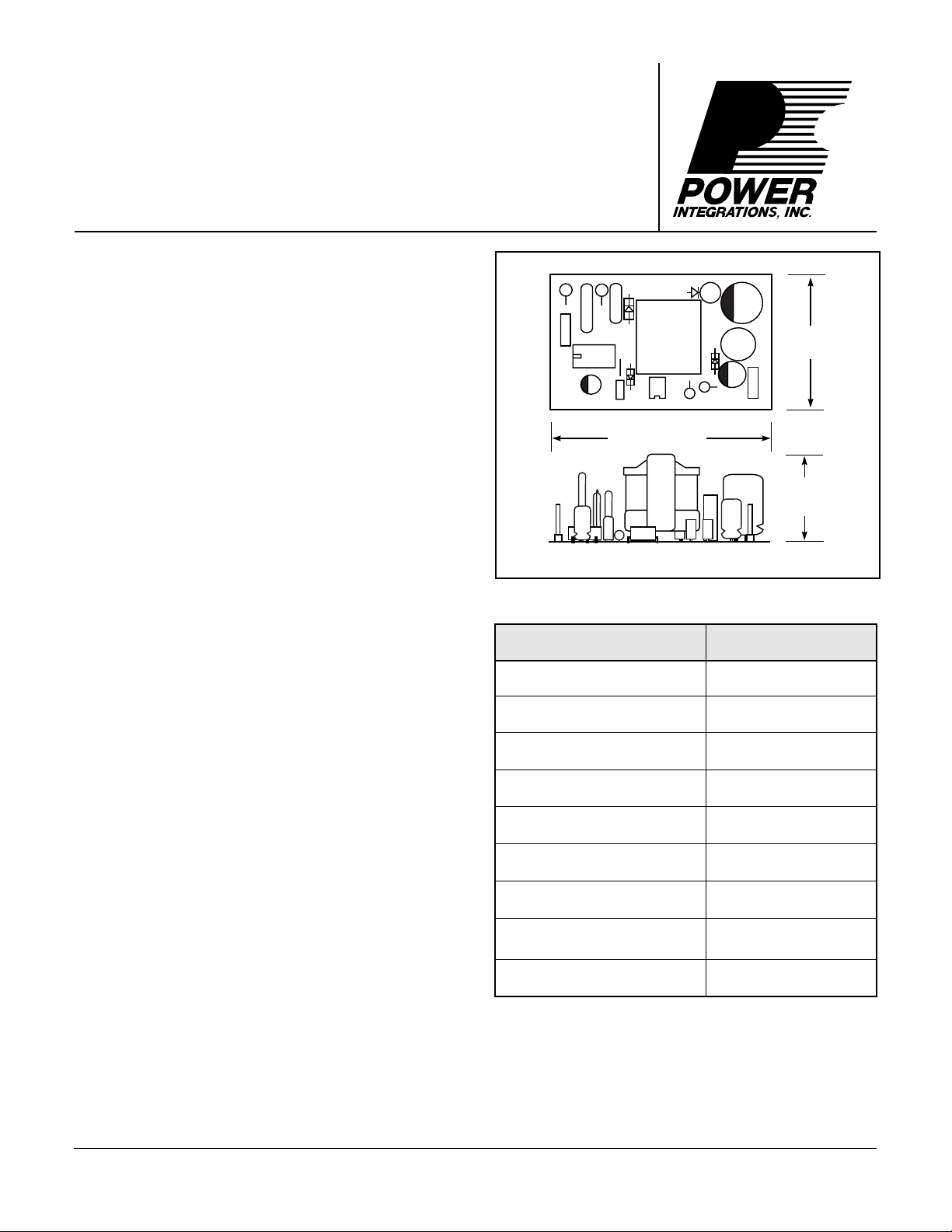
2 in. (48 mm)
®
1.19 in.
(29 mm)
Fully Protected by
• Primary safety current limit
• Output short circuit protection
• Thermal shutdown protects entire supply
Designed for World Wide Operation
• Designed for IEC/UL safety requirements
• Designed for wide range of input voltage
Typical Applications
• Desktop PC stand-by power supply (PS98, ATX, NLX,
SFX, Micro ATX)
• Consumer stand-by supply (e.g. TV, VCR, DVD)
TOPSwitch-II
Description
The RD7 reference design board is an example of a very low
cost production worthy DC input standby power supply design
using the TOPSwitch-II family of Three-terminal Off-line
PWM switchers. The reference design board is intended to help
TOPSwitch-II users quickly develop their products. It provides
a basic design that can be easily modified to fit a particular
application. The RD7 operates from a rectified and filtered AC
mains voltage and provides 3.5 W output at 5 V. Features such
as a 12 V non-isolated output or tighter output voltage tolerance
may be implemented by changing only a few components (See
Figure 4).
.75 in.
(18 mm)
Figure 1. RD7 Overall Physical Dimensions.
PARAMETER
Input Voltage Range 90 to 375 VDC
Temperature Range 0 to 50° C
Output Voltage (I = 0.7 A)
Output Power (continuous) 3.5 W
Line Regulation (90-375VDC) ± 1.0%
Load Regulation (10%-100%) ± 1.0%
Efficiency (At full load) 72%
Output Ripple Voltage ± 50 mV
Safety IEC950/UL1950
Table 1. Table of Key Electrical Parameters.
o
LIMITS
5 V ± 5%
PI-2271-062998
April 1999
Page 2
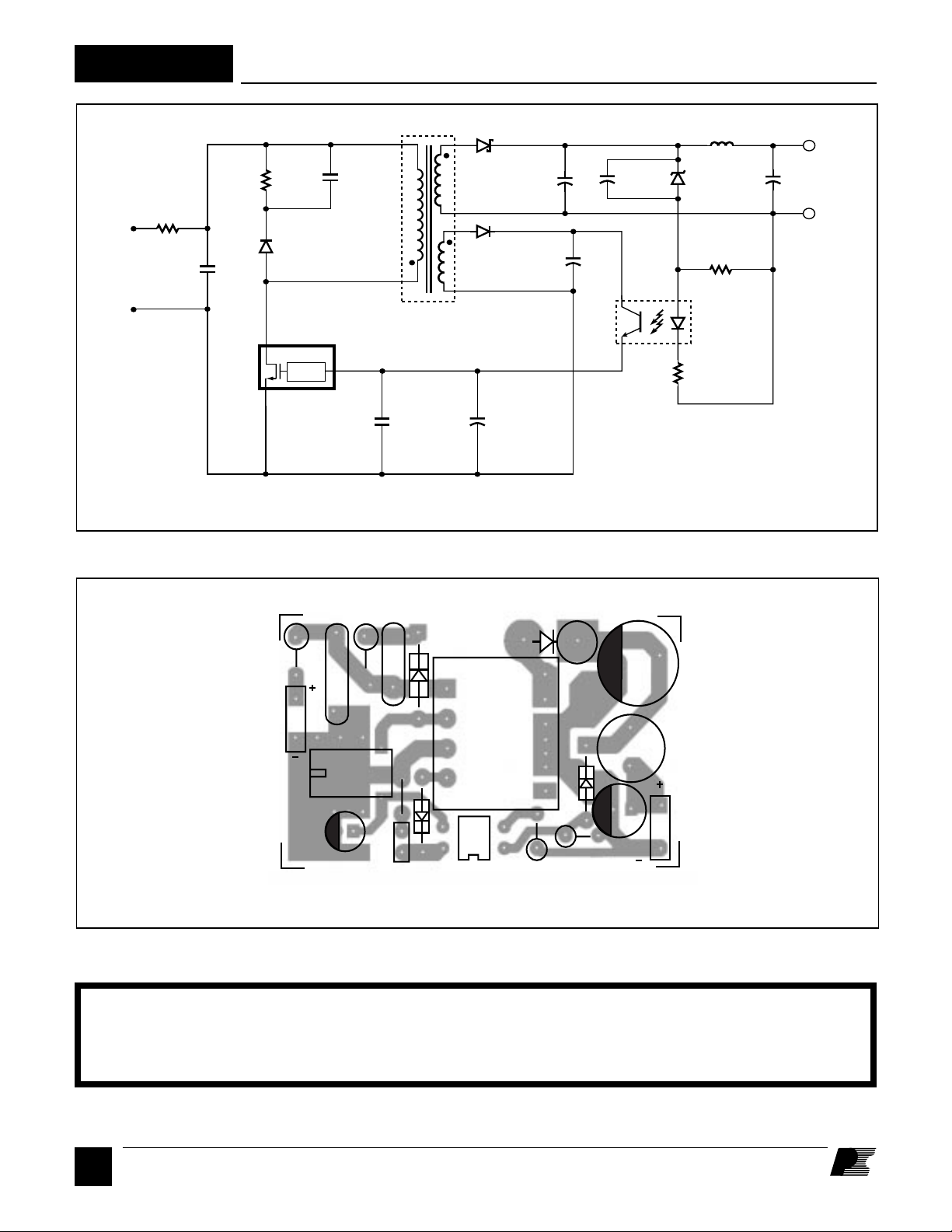
RD7
R1
C1
47 kΩ
D1
UF4005
+
90-375 VDC
Input
RF1
1
Ω
Fusible
10 nF
1 KV
-
D
TOPSwitch-II
CONTROL
S
TOP221P
U1
Figure 2. Schematic diagram of the RD7.
T1
C2
2.2 nF
1 KV
C
C
C
0.1 µF
*
D2
1N5822
D3
1N4148
C3
270 µF
25 V
0.1 µF
50 V
C5
47 µF
10 V
* optional component, not populated
C6
L1
3.3 µH
*
C
ss
VR1
IN5228C
C4
100 µF
25 V
+
5 V – 5%
0.7 A
-
R3
100 Ω
U2
PC817A
R2
10 Ω
PI-2187-062998
RF1
J1
U1
C5
Figure 3. RD7 Pinout and Component Legend.
The RD7 is designed for DC input. Please observe the proper polarity when applying power to this board.
Applying reverse polarity or AC power to the input terminals of the board can damage the TOPSwitch.
D2
U2
R1
C1
C6
S/N
C2
D1
JP1
D3
COMPONENT SIDE SHOWN
CAUTION
R2
R3
T1
VR1
C3
C4
L1
J2
PI-2269-070298
B
2
4/99
Page 3

Component Listing
Reference Value Part Number Manufacturer
C1 10 nF, 1 KV, Disc 5GAS10 Cera-Mite
C2 2.2 nF 1 KV, Disc DD222 Philips
C3 270 µF 25 V ECA-1EFQ271 Panasonic
C4 100 µF 25 V ECE-A1EGE101 Panasonic
C5 47 µF, 10 V ECE-A1AGE470 Panasonic
C6 0.1 µF, 50 V ECU-S1H104MEA Panasonic
Cc* 0.1 µF, 50 V ECU-S1H104MEA Panasonic
Css*
D1 600 V, 1A, UFR UF4005 General Instrument
D2 40 V, 3 A, Schottky 1N5822 General Instrument
D3 75 V, Switching 1N4148 Liteon
L1 3.3 µH, 5 A 622LY-3R3M Toko
RF1 1 Ω Fuse Resistor 1/2 W BW1/2F 1 Ω 5% RCD
R1 47 K, 1/2 W 5053CX47K00J Philips
R2 10 Ω, 1/4 W 5043CX10R00J Philips
R3 100 Ω, 1/4 W 5043CX100R0J Philips
T1** TRD7 Custom
U1 TOP221P or TOP221G*** Power Integrations
U2 Optocoupler, Controlled CTR LTV817A Liteon
VR1 3.9 V, Zener, 2% 1N5228C APD
RD7
Table 2. Parts List For the RD7. (* Optional, for Css values see Figure 9. **T1 is available from Premier Magnetics (714) 362-4211 as P/N
TDS-1185-9818, and from Coiltronics (561) 241-7876 as P/N CTX14-14193-X1. *** TOP221G can be used with layout modifications.)
General Circuit Description
The RD7 is a low-cost, flyback switching power supply using
the TOP221P. The circuit shown in Figure 2 provides a nominal
output power of 3.5 W at 5 VDC output. The power supply
operates from a DC voltage of 90 to 375 VDC. In a typical
application this DC voltage is derived from a rectified and
filtered AC main voltage of 85 to 265 VAC. The 5 V output is
directly sensed by optocoupler U2 and Zener diode VR1. The
output voltage is determined by the Zener diode (VR1) voltage
and the voltage drop across the optocoupler (U2) LED and
resistor R2. Other output voltages are possible by adjusting the
transformer turns ratios and the value of the Zener diode VR1.
The positive rail of the high voltage DC input is connected to
one side of the primary winding of T1. Capacitor C1 filters the
high voltage supply, and is necessary only if the connections
between the high voltage DC supply and the RD7 are long. The
other side of the transformer primary is driven by the integrated,
high-voltage MOSFET inside the TOP221. D1, R1, and C2
clamp voltage spikes caused by transformer leakage inductance
to a safe value and reduce ringing at the DRAIN of U1.
The secondary winding is rectified and filtered by D2 and C3
to generate a 5 V output. L1 and C4 provide additional filtering
to reduce high frequency ripple voltage. R3 and VR1 provide
a slight pre-load on the 5 V output to improve load regulation
at light loads. R3 also provides bias current for Zener VR1 to
improve regulation.
Soft start can be added to eliminate turn-on overshoot. With C
placed across VR1, the optocoupler current is increased during
turn-on time. This increased current limits the duty cycle and
slows down the rising output voltage (See Figure 9). The bias
winding output is rectified and filtered by D3 and C6 to provide
a bias voltage for U2. C5 filters internal MOSFET gate drive
charge current spikes on the CONTROL pin, determines the
auto-restart frequency, and compensates the control loop. Cc is
needed when the supply is operating in a noisy environment
(e. g. when the power supply is sharing the same input rectifier
and filter capacitor with another power supply). Cc filters high
frequency noise.
The schematic of Figure 4 shows an enhanced version of the
RD7. The circuit comprising R2, R3, R4, R5 and U3 improves
overall output regulation to ±2%. Optional soft start capacitor
Css is used to eliminate turn-on overshoot. The bias supply
output can be used to provide a +12 V, non-isolated output by
changing C6 to 100 µF as shown in Figure 4. C6 is added to
reduce output ripple to a primary load.
The circuit performance data shown in Figures 5 to 12 was
ss
4/99
B
3
Page 4
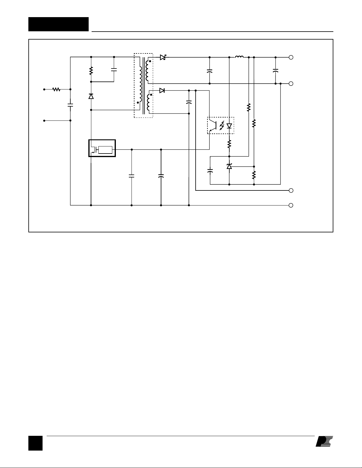
RD7
RF1
1
+
Fusible
90-375 VDC
Input
-
T1
*
D2
1N5822
D3
1N4148
C6
100 µF
35 V
C5
47 µF
10 V
R1
47 kΩ
Ω
D1
UF4005
C1
10 nF
1 KV
D
TOPSwitch-II
CONTROL
S
TOP221P
U1
C2
2.2 nF
1 KV
C
C
C
0.1 µF
C3
270 µF
25 V
C
*
SS
U2
PC817A
L1
3.3 µH
R3
75 Ω
R2
150 Ω
U3
TL431
C4
100 µF
25 V
R4
10 kΩ
R5
10 kΩ
+
5 V – 2%
0.6 A
-
+
12 V
Non-isolated
50 mA
-
*
optional component, not populated
PI-2189-071098
Figure 4. Schematic diagram of the RD7 with 12V Non-isolated output.
measured with DC voltage applied to RD7.
Load Regulation (Figure 5(a) and 5(b)) - The amount of change
in the DC output voltage for a given change in output current is
referred to as load regulation. The 5 V output stay within
±1.0% when the output current is between 0% to 100% of rated
load current at the 5 V output. The TOPSwitch-II overtemperature protection circuit will safely shut down the power
supply under prolonged overload conditions. When the output
load is disconnected, R3 acts as a preload and the output stays
in regulation.
Line Regulation (Figure 6(a) and 6(b)) - The amount of change
in DC output voltage for a given change in the DC input voltage
is called line regulation. The maximum change in output
voltage is within ±1%.
Efficiency (Line Dependent). Efficiency is the ratio of output
power to the input power. The curve in Figure 7 shows how the
efficiency changes with input voltage using a 3.5 W load. The
efficiency is greater than 72% throughout the input range.
Efficiency (Load Dependent). The curves in Figure 8 show
how the efficiency changes with output power at 155 and 310
VDC inputs. The efficiency is greater than 70% for loads
greater than 2.5 W.
Power Supply Turn On Sequence. An internal switched, high
voltage current source provides the initial bias current for
TOPSwitch when power is first applied. The waveforms shown
in Figure 8 illustrates the timing relationship between the high
voltage DC bus and 5 V output voltage for the RD7 circuit.
Capacitor C1 charges to the DC input voltage before TOPSwitch
turns on. The delay of 130 ms (typical) is caused by the time
required to charge the auto-restart capacitor C5 to 5.7 V. At this
point the power supply turns on as shown.
Figure 10 shows the output voltage turn on transient as well as
a family of curves associated with the additional soft-start
capacitor Css. The soft-start capacitor is placed across VR2 and
can range in value from 10 µF to 47 µF as shown.
Switching frequency ripple voltage is shown in Figure 11 for
the RD7 circuit at 155 VDC input and 3.5 W output. Peak to
peak ripple is less than 50 mV at 3.5 W.
The RD7 power supply transient response to a step load change
from 0.52 A to 0.75 A (75% to 100%) is shown in Figure 12.
The response is quick and well damped.
The RD7 is designed to meet worldwide safety specifications.
B
4
4/99
Page 5

RD7
(b) Input Voltage (VDC)
Output Voltage (% of Nominal)
PI-2233-071098
80 240 400
100
100
95
95
105
105
(a) Input Voltage (VDC)
80 240 400
Thermal Considerations
The RD7 utilizes the printed circuit copper for TOPSwitch-II
heatsinking. With a copper area of approximately 0.227 in
(1.46 cm2 ) and 2 oz. (610 g/m2) copper cladding, the temperature
of the TOPSwitch-II rises 6 oC at 50 oC ambient temperature
and 3.5 W load.
Transformer Specifications
The electrical specifications and construction details for
transformer TRD7 are shown in Figures 13 and 14. Transformer
TRD7 is supplied with the RD7 reference design board. This
design utilizes an EE16 core and a triple insulated wire secondary
105
100
95
105
0 100
200
300
(a) 5 V Load Current (mA)
VIN = 155 VDC
400
500
VIN = 310 VDC
600
PI-2231-071098
700
winding. The use of triple insulated wire allows the transformer
to be constructed using a smaller core and bobbin than a conventional magnet wire design due to the elimination of the creepage
2
margins required for safety spacing in a conventional design.
If a conventional margin wound transformer is desired, the
design of Figures 15 and 16 can be used. This design (TRD7-1)
uses an EEL16 core and bobbin to accommodate the 6 mm
creepage required to meet international safety standards when
using magnet wire rather than triple insulated wire, and has the
same pinout and printed circuit foot print as TRD7. The
transformer is approximately 50% taller than the triple insulated
wire design due to the inclusion of creepage margins required
to meet international safety standards.
100
Output Voltage (% of Nominal)
95
0 100
200
(b) 5 V Load Current (mA)
Figure 5 (a). Load Regulation at 155 VDC Input Voltage.
(b). Load Regulation at 310 VDC Input Voltage.
300
600
400
500
80
70
60
50
700
Efficiency (%)
40
30
80 240 400
Po = 3.5 W
Input Voltage (VDC)
Figure 7. Efficiency vs. Input Voltage, 3.5 W Output.
Figure 6 (a). Line Regulation at 3.5 W Output.
(b). Line Regulation at 0.35 W Output.
PI-2235-062998
4/99
B
5
Page 6

RD7
PI-2245-071098
0
10 20
400
- 50
0
600
Output Voltage (mV)
Time (ms)
50
100
200
0
Output Current (mA)
80
150
100
50
0
4
2
60
40
20
Efficiency (%)
0
DC BUS VOLTAGE
OUTPUT
VOLTAGE
0.0
0.5 1.0 1.5
Output Power (W)
Figure 8. Efficiency vs. Output Power.
PI-2239-060498
VIN = 155 VDC
VIN = 310 VDC
2.0 2.5 3.0 3.5
6
5
4
3
2
Output Voltage (V)
1
0 µF
10 µF
PI-2237-060398
22 µF
PI-2241-060498
47 µF
0
0
Figure 9. Turn on Delay. Figure 10. Output Voltage Turn On Transient vs. Soft Start Capacitor.
200
150
100
50
0
-50
Output Voltage (mV)
-100
-150
-200
0
Figure 11. Switching Frequency Ripple, 155 VDC Input, 3.5 W Output.
100 200
Time (ms)
25 50
Time (µs)
0
0
10 20
Time (ms)
PI-2243-062998
Figure 12. Transient Load Response (75% to 100% of load).
B
6
4/99
Page 7

TRIPLE INSULATED SECONDARY TRANSFORMER (TRD1)
1
116 T
#37 AWG
2
3
14 T
#37 AWG
4
CORE# - PC40 EE16-Z (TDK)
GAP FOR AL OF 182 nH/T
9, 10
6 T
#26 AWG
Triple-insulated
6, 7
2
BOBBIN# - YW-193 (Yih Hwa Enterprises)
ELECTRICAL SPECIFICATIONS
PIN FUNCTION
1
HIGH-VOLTAGE DC BUS
2
3
4
6, 7
9, 10
TOPSwitch
PRIMARY-SIDE COMMON
V
BIAS
SECONDARY RETURN
OUTPUT
DRAIN
RD7
4
1
5
10
Electrical Strength
Creepage
Primary Inductance
Resonant Frequency
Primary Leakage Inductance
NOTE: All inductance measurements should be made at 100 kHz
Figure 13. Electrical Specification of Transformer TRD7.
60 Hz, 1 minute,
from pins 1-4 to pins 5-10
Between pins 1-4 and pins 5-10
All windings open
All windings open
Between pins 1-2 (pins 6-10 shorted)
3000 VAC
6.00 mm (min)
2430 µH –10%
500 kHz (min)
63 µH (max)
PI-2273-070298
4/99
B
7
Page 8

RD7
TRIPLE INSULATED SECONDARY TRANSFORMER CONSTRUCTION
TAPE
TAPE
{
{
6, 7
9, 10
3
4
1
2
WINDING INSTRUCTIONS
Primary
Basic Insulation
Bias Winding
Basic Insulation
Secondary Winding
SECONDARY
BIAS
PRIMARY
Start at Pin 2. Wind one complete layer (about 58 turns)
of 37 AWG heavy nyleze wire from left to right. Insulate
first layer using 1 turn of polyester film tape, 8.3 mm
wide, 0.056 mm thick. Wind remaining 58 turns from
right to left for a total of 116 turns. Finish at Pin 1.
Apply 1 layer of tape for basic insulation.
Start at Pin 4. Wind 14 turns parallel bifilar of 37 AWG
wire from left to right in a single layer. Finish at Pin 3.
Apply 1 layer of tape for basic insulation.
Start at Pins 9, 10. Wind 6 turns parallel bifilar of 26 AWG
triple insulated wire from left to right. Finish on Pin 6, 7.
Outer Insulation
Final Assembly
* Triple insulated wire sources.
P/N: T27A01TXXX-3
Rubudue Wire Company
5150 E. La Palma Avenue
Suite 108
Anaheim Hills, CA 92807
(714) 693-5512
(714) 693-5515 FAX
Figure 14. Construction Details of Transformer TRD7.
B
8
4/99
P/N: order by description
Furukawa Electric America, Inc.
200 Westpark Drive
Suite 190
Peachtree City, GA 30269
(770) 487-1234
(770) 487-9910 FAX
Apply 3 layers of tape for basic insulation.
Assemble and secure core halves.
Impregnate uniformly with varnish.
P/N: order by description
The Furukawa Electric Co., Ltd
6-1, Marunouchi 2-chome,
Chiyoda-ku, Tokyo 100, Japan
81-3-3286-3226
81-3-3286-3747 FAX
PI-2275-070298
Page 9

RD7
MARGIN WOUND TRANSFORMER
1
116 T
#35 AWG
2
3
14 T
35 AWG
4
CORE# - PC40 EE16/24/5-Z (TDK)
GAP FOR AL OF 182 nH/T
9, 10
6 T
#26 AWG
6, 7
2
BOBBIN# - YW-035 (Yih Hwa Enterprises)
ELECTRICAL SPECIFICATIONS
Electrical Strength
Creepage
Primary Inductance
PIN FUNCTION
1
HIGH-VOLTAGE DC BUS
2
TOPSwitch DRAIN
3
PRIMARY-SIDE COMMON
4
V
BIAS
6, 7
9,10
RETURN
OUTPUT
60 Hz, 1 minute,
from pins 1-4 to pins 5-10
Between pins 1-4 and pins 5-10
All windings open
10
1
3000 VAC
6.0 mm (min)
2430 µH –10%
5
4
Resonant Frequency
Primary Leakage Inductance
Between pins 1-2 (pins 6-10 shorted)
NOTE: All inductance measurements should be made at 100 kHz
Figure 15. Electrical Specification of Transformer TRD7-1.
All windings open
300 kHz (min)
70 µH (max)
PI-2277-062998
4/99
B
9
Page 10

RD7
MARGIN WOUND TRANSFORMER CONSTRUCTION
TAPE
TAPE
WINDING INSTRUCTIONS
{
{
SLEEVING
6, 7
9, 10
4
1
2
TAPE MARGINS
(4 PLACES)
SECONDARY
3
BIAS
PRIMARY
Safety Margin
Primary
Basic Insulation
Bias Winding
Reinforced Insulation
Safety Margin
Construct margins on each side of bobbin using 3 mm
wide tape. Match height of primary plus bias winding.
Start at Pin 2. Wind one complete layer (about 58 turns)
of 35 AWG heavy nyleze wire from left to right between
margins. Insulate first layer using 1 layer of polyester
tape (polyester film 11.5 mm (0.456 in) wide and 0.056
(2.2 mil) thick) for basic insulation. Wind remaining 58 turns
in second layer from right to left. Finish on Pin 1. Sleeve
start and finish leads using safety approved insulating
sleeving with 0.4 mm (0.016 in) minimum wall thickness.
Apply 1 layer of 11.5 mm wide tape for basic insulation.
Start at Pin 4. Wind 14 parallel bifilar turns of 35 AWG
heavy nyleze wire from left to right in a single layer.
Finish on Pin 3. Sleeve start and finish leads as above.
Apply 3 layers of tape (polyester film, 17.5 mm (0.689 in)
wide and 0.056 mm (2.2 mil) thick) for reinforced
insulation.
Construct margins on each side of bobbin using 3 mm
wide tape. Match height of secondary winding.
Secondary Winding
Outer Insulation
Final Assembly
Figure 16. Contruction Details of Transformer TRD7-1.
B
10
4/99
Start at Pin 9 and 10. Wind 6 parallel bifilar turns of 26 AWG
heavy nyleze wire from left to right in a single layer. Finish
on Pin 6 and 7. Sleeve start and finish leads as above.
Apply 3 layers of 17.5 mm tape for outer insulation.
Assemble and secure core halves. Impregnate
uniformly with varnish.
PI-2281-062998
Page 11

RD7
4/99
B
11
Page 12

RD7
Revision
A
B
Notes
Measurement method for primary leakage inductance of TRD7 and TRD7-1 corrected.
Date
9/98
4/99
Power Integrations reserves the right to make changes to its products at any time to improve reliability or manufacturability.
Power Integrations does not assume any liability arising from the use of any device or circuit described herein, nor does it
convey any license under its patent rights or the rights of others.
PI Logo and
TOPSwitch
are registered trademarks of Power Integrations, Inc.
©Copyright 1998, Power Integrations, Inc. 477 N. Mathilda Avenue, Sunnyvale, CA 94086 http://www.powerint.com
WORLD HEADQUARTERS
NORTH AMERICA - WEST
Power Integrations, Inc.
477 N. Mathilda Avenue
Sunnyvale, CA 94086 USA
Main: +1•408•523•9200
Customer Service:
Phone: +1•408•523•9265
Fax: +1•408•523•9365
KOREA
Power Integrations International
Holdings, Inc.
Rm# 402, Handuk Building,
649-4 Yeoksam-Dong, Kangnam-Gu,
Seoul, Korea
Phone: +82•2•568•7520
Fax: +82•2•568•7474
NORTH AMERICA - EAST
& SOUTH AMERICA
Power Integrations, Inc.
Eastern Area Sales Office
1343 Canton Road, Suite C1
Marietta, GA 30066 USA
Phone: +1•770•424•5152
Fax: +1•770•424•6567
JAPAN
Power Integrations, K.K.
Keihin-Tatemono 1st Bldg.
12-20 Shin-Yokohama 2-Chome,
Kohoku-ku, Yokohama-shi,
Kanagawa 222, Japan
Phone: +81•(0)•45•471•1021
Fax: +81•(0)•45•471•3717
EUROPE & AFRICA
Power Integrations (Europe) Ltd.
Centennial Court
Easthampstead Road
Bracknell
Berkshire RG12 1YQ,
United Kingdom
Phone: +44•1344•462•300
Fax: +44•1344•311•732
INDIA (Technical Support)
Innovatech
#1, 8th Main Road
Vasanthnagar
Bangalore 560052, India
Phone: +91•80•226•6023
Fax: +91•80•228•2191
TAIWAN
Power Integrations International
Holdings, Inc.
2F, #508, Chung Hsiao E. Rd., Sec. 5,
Taipei 105, Taiwan
Phone: +886•2•2727•1221
Fax: +886•2•2727•1223
APPLICATIONS HOTLINE
World Wide +1•408•523•9260
APPLICATIONS FAX
World Wide +1•408•523•9361
12
B
4/99
 Loading...