

Page 1
®
RD2
TOPSwitch
Reference Design Board
85 to 132 VAC or 170 to 265 VAC Input,
8W(10W Peak) Output
Product Highlights
Low Cost Production Worthy Reference Design
• Only 21 components!
• Single sided board
• Low cost thru-hole components
• Fully assembled and tested
• Easy to evaluate and modify
• Extensive performance data
• Up to 77% efficiency
• Light weight - no heat sink required for TOPSwitch
®
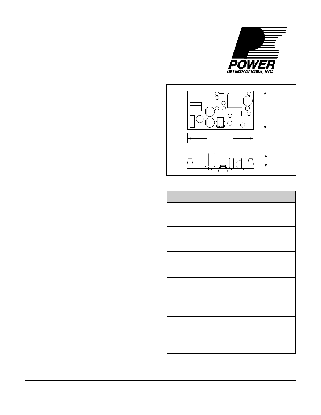
1.4 in.
2.6 in.
Fully Protected by
• Primary safety current limit
• Output short circuit protection
• Thermal shutdown protects entire power supply
Designed for World Wide Operation
• Designed for IEC/UL safety requirements
• Meets VDE Class B EMI specifications
Typical Applications
• Replacement for low power linear adapters
• Auxiliary power supply for appliance, motor control,
utility meters, smart building, UPS, etc.
TOPSwitch
Description
The RD2 reference design board is an example of a very low
cost production worthy power supply design using the
TOPSwitch family of Three-terminal Off-line Switchers from
Power Integrations. It is intended to help TOPSwitch users to
quickly develop their products by providing a basic design that
can be easily modified to fit a particular application. In most
cases, a minor change to the transformer for a different output
voltage or voltages is all that is needed. A complete set of
performance curves, the parts list, the board layout and details
on transformer design are provided to speed up the TOPSwitch
based switcher design.
0.8 in.
Figure 1. RD2 Board Overall Physical Dimensions.
PARAMETER LIMITS
Input Voltage Range
Input Frequency Range 47 to 440 Hz
Temperature Range 0 to 70°C
Output Voltage (I = 0.67A) 12 V ± 10%
Output Power (continuous) 8 W
Output Power (peak) 10 W
Line Regulation ± 0.7%
Load Regulation (10%-100%) ± 5%
Efficiency (115 V input, 8 W out) 75%
Output Ripple Voltage ± 50 mV MAX
o
(85-132 VAC)
(170-265 VAC)
85 to 132 VAC
85 to 132 VAC
or 170 to 265 VAC
PI-1768-020596
Safety IEC 950 / UL1950
EMI
Figure 2. Table of Key Electrical Parameters.
VDE B (VFG243 B)
CISPR22
May 1996
Page 2
RD2
C6
47nF
250VAC
X2
L
N
J1
+
-
F1
2A
BR1
DF06M
JUMPER
L2
8 mH
0.2A
470 KΩ
JP1*
RB
470 KΩ
RA
C9
10 µF
200 V
VR1
C1
+
BZY97-C200
10 µF
200 V
D1
UF4005
+
+
R1
6.8 Ω
C5
47 µF
U1
DC
TOP
210
SS
10 V
* JPI CLOSED FOR 115 VAC INPUT
JPI OPEN FOR 230 VAC INPUT
D3
1N4148
250 VAC
1
2
4
3
C7
1nF
Y1
T1
T1RD2
D2
MBR360
8
C2
++
330 µF
16 V
5
L1
3.3 µH
C3
120 µF
16 V
12 V
R2
390 Ω
1W
RTN
PI-1783-020596
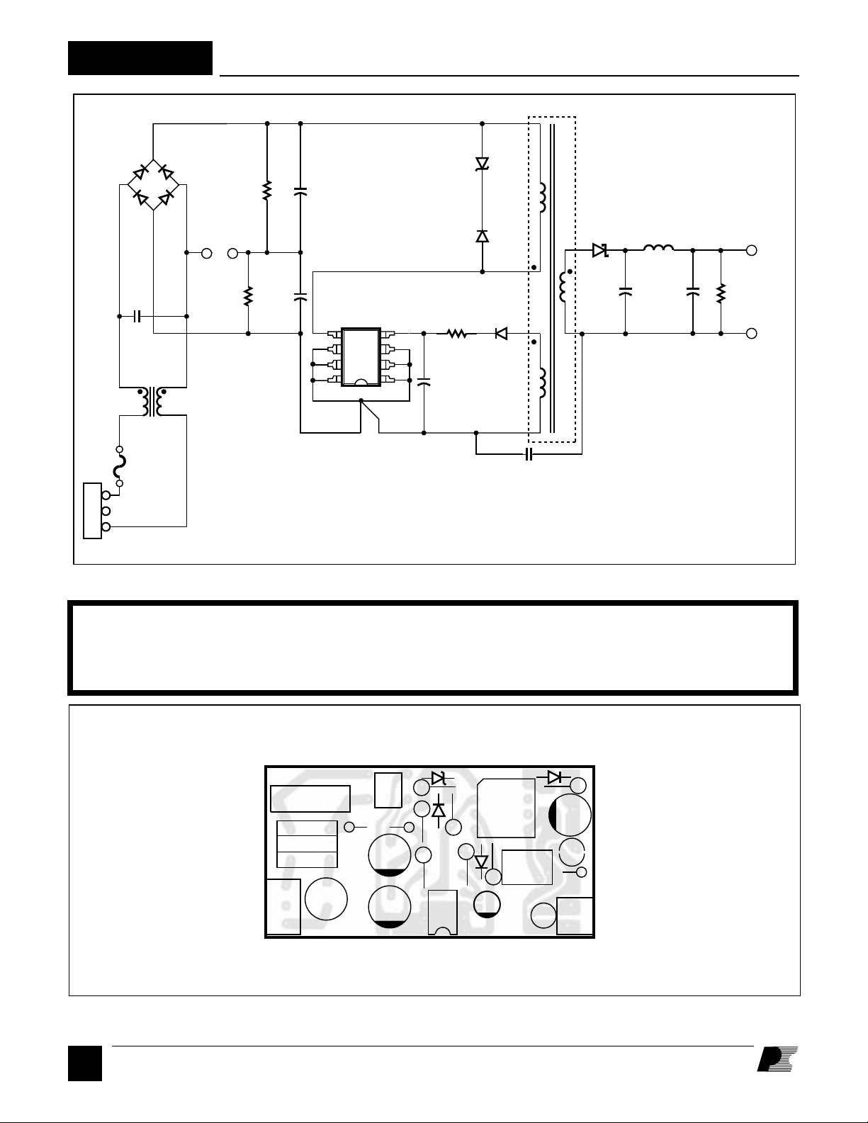
Figure 3. Schematic Diagram of the RD2 Power Supply.
CAUTION
The RD2 features a 115/230 VAC selectable input, and is shipped configured for 230 VAC operation (JP1 open).
If JP1 is used for 115 VAC operation, it must be removed before applying 230 VAC.
C6
L2
F1 C1
N
TOPSwitch
L
BR1
RD2
JP1
C9 8
-
+
RA
RB
+
U1
VR1
D1
R1
D2
C2
D3 T1
+
-
C5
C7
C3
+
R2
+
L1+
+
PI-1817-040296
Figure 4. Component Legend of the RD2.
B
2
5/96
Page 3

Component Listing
Reference Value Part Number Manufacturer
U1 TOP210PFI Power Integrations
D1 600V, 1A, UFR UF4005 General Instruments
D2 Schottky, 3A, 60V MBR360 Motorola
D3 75 V Switching 1N4148 Rohm
BR1 1 A, 600 V DF06M General Instruments
VR1 200 V Zener, 1.5 W BZY97-C200 SGS/Thomson, Fagor
L1 3.3 µH, 4A Custom
L2 8 mH, 0.2A SU9V-02080 Tokin
C1, C9 10 µF, 200V KMG200VB10RM10X16 United Chemicon
C2 330 µF, 16V LXF16VB331M8X15 United Chemicon
C3 120 µF, 16V LXF16VB121M6.3X11.5 United Chemicon
C5 47 µF, 10V KME10VB47RM5X12.5 United Chemicon
C6 47 nF, 250 VAC, X 2 F1772-347-2000 Roederstein
C7 1 nF, 250 VAC, Y1
RA, RB 470 K, 1/4 W 5043CX470K0J Philips
R1 6.8 Ω, 1/4 W 5043CX6R800J Philips
R2 390 ohms, 1 W MO-1 391J Koa/Speer
T1 Custom T1RD2
F1 2A, 250 VAC 19372, 2A Wickman
DE1110 E 102M ACT4K-KD
RD2
Murata
Figure 5. Parts List for the RD2.
General Circuit Description
The RD2 is a low-cost, isolated Buck-Boost or flyback switching
power supply using the TOP210 integrated circuit. The circuit
shown in Figure 3 produces a 12 V, 8 W power supply that
operates from 85 to 132 VAC or 170 to 264 VAC input voltage.
The 12 V output voltage is determined by the TOPSwitch
control pin shunt regulator voltage, the voltage drop of D3, and
the turns ratio between the bias and output windings of T1.
Other output voltages are also possible by adjusting the
transformer turns ratios. R1 and C5 provide filtering of the bias
winding to improve line and load regulation.
AC power is rectified and filtered by BR1, C1 and C9 to create
the high voltage DC bus applied to the primary winding of T1.
The other side of the transformer primary is driven by the
integrated high-voltage MOSFET inside the TOP210. JP1 is
a jumper used to select 115 V or 230 V operation. Adding JP1
selects 115 V operation. Leaving JP1 open selects 230 V
operation. RD2 is supplied with JP1 open. RA and RB equalize
leakage currents between C1 and C9. D1 and VR1 clamp the
leading-edge voltage spike caused by transformer leakage
inductance to a safe value and reduce ringing. The power
secondary winding is rectified and filtered by D2, C2, L1, and
C3 to create the 12 V output voltage. R2 provides a pre-load on
the 12 V output to improve load regulation at light loads. The
bias winding is rectified and filtered by D3, R1, and C5 to create
a bias voltage to the TOP210. Common-mode EMI currents
which flow between the primary windings of the transformer
and the secondary output circuitry are attenuated by L2 and C7.
Differential-mode EMI currents caused by pulsating currents at
the input of the power supply are attenuated by C6 and L2. C5
filters the internal MOSFET gate drive charge current spikes on
the Control pin, determines the auto-restart frequency, and
together with R1, compensates the control loop.
The circuit performance data shown in Figures 6-18 was
measured with AC voltage applied to the RD2.
Load Regulation (Figure 6) - The amount of change in the DC
output voltage for a given change in output current is referred
to as load regulation. The 12 V output stays within ±5% from
10% to 100% of rated load current. The TOPSwitch on-chip
overtemperature protection circuit will safely shut down the
power supply under sustained overload conditions.
5/96
B
3
Page 4
RD2
General Circuit Description (cont.)
Line Regulation (Figure 7) - The amount of change in the DC
output voltage for a given change in the AC input voltage is
called line regulation. The maximum change in output voltage
is less than ±0.7%.
Efficiency (Line Dependent) - Efficiency is the ratio of the
output power to the input power. The curves in Figures 8 and 9
show how the efficiency changes with input voltage. Curves
are also given to show the difference in efficiency when C1 and
C9 are changed from 10 µF to 22 µF.
Efficiency (Load Dependent) - The curves in Figures 10 and 11
show how the efficiency changes with output power at 115 and
230 VAC inputs. The curves also show the increase in efficiency
when C1 and C9 are changed from 10 µF to 22 µF.
Power Supply Turn On Sequence - The internal switched, highvoltage current source provides the initial bias current for
TOPSwitch when power is first applied. The waveforms shown
in Figure 12 illustrate the relationship between the high-voltage
DC bus and 12 V output voltage. Capacitors C1 and C9 charge
to the peak of the AC input voltage before TOPSwitch turns on.
The delay of 150 ms (typical) is caused by the time required to
charge the auto-restart capacitor C5 to 5.7 V. At this point the
power supply turns on as shown.
Figure 13 shows the output voltage turn on transient.
Line frequency ripple voltage is shown in Figure 14 for
115 VAC input and 8W output. Switching frequency ripple
voltage is shown in Figure 15 for the same test condition.
The power supply transient response to a step load change from
0.5 A to 0.67 A (75% to 100%) is shown in Figure 16. Note that
the response is quick and well damped.
The RD2 is designed to meet worldwide safety and EMI
(VDE B) specifications. Measured conducted emissions are
shown in Figure 17 for 115 VAC and Figure 18 for 230 VAC.
105
100
95
0
100
200 300
VIN = 115 VAC
PI-1769-020596
400 500 600 700
Load Current (mA)
105
100
Output Voltage (% of Nominal)
95
0
100
200 300
VIN = 230 VAC
400 500 600 700
Load Current (mA)
Figure 6. Load Regulation Figure 7. Line Regulation
B
4
5/96
101
100.5
100
99.5
99
90 100 110 120 130
Input Voltage (VAC)
101
100.5
100
Output Voltage (% of Nominal)
99.5
99
I
= 0.67 A
OUT
I
= 0.17 A
OUT
180 200 220 240 260
Input Voltage (VAC)
I
OUT
I
OUT
= 0.67 A
= 0.17 A
PI-1770-020596
Page 5

RD2
60
170 190 210 250 270230
Input Voltage (VAC)
Output Efficiency (%)
PI-1772-020596
70
80
75
65
I
OUT
= 0.17 A
I
OUT
= 0.67 A, C1, C9 = 22 µF
I
OUT
= 0.17 A, C1, C9 = 22 µF
I
OUT
= 0.67 A
60
123 56784
Output Power (W)
Output Efficiency (%)
PI-1774-020596
70
80
75
65
VIN = 230 VAC
VIN = 230 VAC, C1, C9 = 22 µF
80
PI-1771-020596
75
I
= 0.67 A
OUT
I
= 0.67 A, C1, C9 = 22 µF
70
65
Output Efficiency (%)
60
85 95 105 125 135115
Figure 8. Efficiency vs. Input Voltage, 85-132 VAC Figure 9. Efficiency vs. Input Voltage, 170-265 VAC
80
OUT
I
= 0.17 A
OUT
I
= 0.17 A, C1, C9 = 22 µF
OUT
Input Voltage (VAC)
75
70
65
Output Efficiency (%)
VIN = 115 VAC
VIN = 115 VAC, C1, C9 = 22 µF
60
123 56784
Output Power, (W)
Figure 10. Efficiency vs. Output Power, 115 VAC Input
DC BUS VOLTAGE
300
200
100
0
15
10
5
OUTPUT
VOLTAGE
PI-1773-020596
Figure 11. Efficiency vs. Output Power, 230 VAC Input
PI-1775-020596
12
10
8
6
Output Voltage (V)
4
2
PI-1776-020596
0
0
Figure 12. Turn On Delay Figure 13. Output Voltage Turn On Transient
250 500
Time (ms)
0
0
25 50
Time (ms)
B
5
5/96
Page 6

RD2
PI-1777-020596
0
25 50
-40
20
0
40
-20
Output Voltage (mV)
Time (µ sec)
40
20
0
-20
Output Voltage (mV)
-40
0
10 20
Time (m sec)
Figure 14. Line Frequency Ripple, 115VAC In, 8W Output
50
0
-50
Output Voltage (mV)
0.8
PI-1778-020596
Figure 15. Switching Frequency Ripple, 115 VAC In, 8W Output
PI-1779-020696
Figure 17. EMI Characteristics at 115 VAC Input.
Amplitude (dBµV)
100
80
60
40
20
0
0.01 0.1
0.6
0.4
0.2
0
Output Current (A)
01020
Figure 16. Transient Load Response (75% to 100% of load)
VDE B Limit
(VFG243)
1
Frequency (MHz)
10
PI-1818-040296
Time (ms)
100
80
60
40
Amplitude (dBµV)
20
0
0.01 0.1
Frequency (MHz)
Figure 18. EMI Characteristics at 230 VAC Input.
VDE B Limit
(VFG243)
1
PI-1819-040296
10
B
6
5/96
Page 7

RD2
1
130 T
#38 AWG
2
3
6 T
2X #28 AWG
Triple Insulated
4
8
12 T
#26 AWG
Triple Insulated
5
CORE# - PC40 EE16 (TDK)
GAP FOR AL OF 250 nH/T
2
BOBBIN# - BE-16-118CPH (TDK)
ELECTRICAL SPECIFICATIONS
Electrical Strength
Creepage
Primary Inductance
PIN FUNCTION
1
HIGH-VOLTAGE DC BUS
2
TOPSwitch
3
PRIMARY-SIDE COMMON
4
V
BIAS
5
RETURN
8
OUTPUT
60 Hz, 1 minute,
from pins 1-4 to pins 5, 8
Between pins 1-4 and pins 5, 8
All windings open
DRAIN
8
1
1
3000 VAC
5.0 mm (min)
4.3 mH, ±10%
5
4
4
Resonant Frequency
Primary Leakage Inductance
NOTE: All inductance measurements should be made at 100 kHz
Figure 19. Electrical specification of transformer T1RD2
All windings open
Pins 5 and 8 shorted
700 kHz (min)
50 µH (max)
PI-1820-040296
5/96
B
7
Page 8

RD2
BIAS
TAPE
{
PRIMARY
WINDING INSTRUCTIONS
3
4
5
8
1
2
SECONDARY
}
TAPE
Two-layer "C" Wound Primary
Basic Insulation
Triple Insulated Secondary
Basic Insulation
Parallel Bifilar Primary Bias
Outer Insulation
Final Assembly
* Triple insulated wire sources.
P/N: order by description
Rubudue Wire Company
5150 E. La Palma Avenue
Suite 108
Anaheim Hills, CA 92807
(714) 693-5512
(714) 693-5515 FAX
Start at pin 2. Wind 65 turns of 38 AWG heavy nyleze
wire from left to right. Apply 1 layer of tape (white
polyester film 8.3 mm (0.32 in.) wide by 0.056 mm
(2.2 mil) thick) for basic insulation. Continue winding
65 turns from right to left. Finish at pin1.
Apply 2 layers of tape for basic insulation.
Start at pin 8. Wind12 turns of triple-insulated
26 AWG wire* from right to left.
Finish at pin 5.
Apply 2 layers of tape for basic insulation.
Start at pin 4. Wind 6 turns of 28 AWG triple insulated
wire* parallel bifilar in a single layer, from left to right.
Finish at pin 3.
Apply 3 layers of tape for basic insulation.
Assemble and secure core halves.
Impregnate uniformly with varnish.
P/N: order by description
Furukawa Electric America, Inc.
200 Westpark Drive
Suite 190
Peachtree City, GA 30269
(770) 487-1234
(770) 487-9910 FAX
P/N: order by description
The Furukawa Electric Co., Ltd
6-1, Marunouchi 2-chome,
Chiyoda-ku, Tokyo 100, Japan
81-3-3286-3226
81-3-3286-3747 FAX
PI-1740-010596
Figure 20. Construction details of transformer T1RD2
B
8
5/96
Page 9

Notes
RD2
5/96
B
9
Page 10

RD2
Notes
10
B
5/96
Page 11

Notes
RD2
5/96
B
11
Page 12

RD2
Power Integrations reserves the right to make changes to its products at any time to improve reliability or manufacturability.
Power Integrations does not assume any liability arising from the use of any device or circuit described herein, nor does it
convey any license under its patent rights or the rights of others.
PI Logo and
TOPSwitch
are registered trademarks of Power Integrations, Inc.
©Copyright 1994, Power Integrations, Inc. 477 N. Mathilda Avenue, Sunnyvale, CA 94086
WORLD HEADQUARTERS
Power Integrations, Inc.
477 N. Mathilda Avenue
Sunnyvale, CA 94086
USA
Main: 408•523•9200
Customer Service:
Phone: 408•523•9265
Fax: 408•523•9365
JAPAN
Power Integrations, Inc.
Keihin-Tatemono 1st Bldg.
12-20 Shin-Yokohama 2-Chome.Kohoku-ku
Yokohama-shi, Kanagawa 222
Japan
Phone: 81•(0)•45•471•1021
Fax: 81•(0)•45•471•3717
AMERICAS
For Your Nearest Sales/Rep Office
Please Contact Customer Service
Phone: 408•523•9265
Fax: 408•523•9365
ASIA & OCEANIA
For Your Nearest Sales/Rep Office
Please Contact Customer Service
Phone: 408•523•9265
Fax: 408•523•9365
EUROPE & AFRICA
Power Integrations (Europe) Ltd.
Mountbatten House
Fairacres
Windsor SL4 4LE
United Kingdom
Phone: 44•(0)•1753•622•208
Fax: 44•(0)•1753•622•209
APPLICATIONS HOTLINE
World Wide 408•523•9260
APPLICATIONS FAX
Americas 408•523•9361
Europe/Africa
44•(0)•1753•622•209
Japan 81•(0)•45•471•3717
Asia/Oceania 408•523•9364
12
B
5/96
 Loading...