

Page 1
www.fairchildsemi.com
RC5060
ACPI Switch Controller
Features
¥ Implements ACPI control with PWROK, SLP_S3# and
SLP_S5 #
¥ Switch and linear regulator controller for 3.3V Dual (PCI)
¥ Linear regulator controller and linear regulator for 2.5V
Dual (RAMBUS)
¥ Two switch controller for 5V Dual (USB)
¥ Switch controller and linear regulator for 3.3V SDRAM
¥ Provides SDRAM and RAMBUS power simultaneously
¥ Adaptive Break-before-Make
¥ Integrated Power Good
¥ Drives all N-Channel MOSFETs plus NPN
¥ Latched overcurrent protection for outputs
¥ Power-up softstarts for the linear regulators
¥ UVLO guarantees correct operation for all conditions
¥ 20 pin SOIC package
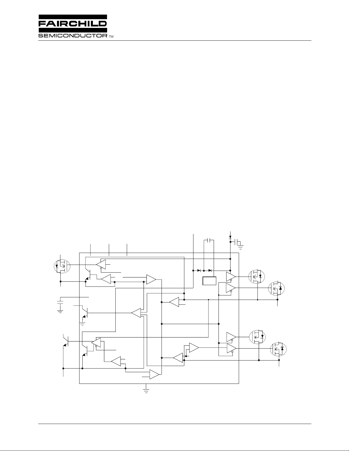
Block Diagram
3.3V Main
3.3V SDRAM
3
4
13
9
PWROK
12
Softstart
PWRGD
SLP_S3#
10
+
-
SLP_S5#
Over Current
Ref
11
+
-
Applications
¥ Camino Platform ACPI Controller
¥ Whitney Platform ACPI Controller
¥ Tehama Platform ACPI Controller
Description
The RC5060 is an ACPI Switch Controller for the Camino,
Whitney and Tehama Platforms. It is controlled by PWROK,
SLP_S3# and SLP_S5#, and provides 3.3V Dual for PCI, 3.3V
for SDRAM, 2.5V Dual for RAMBUS, and 5V Dual voltages.
An on-board precision low TC reference achieves tight tolerance voltage regulation without expensive external components.
The RC5060 also offers integrated Power Good and Current
Limiting that protects each output, and softstart for the linear
regulators. The RC5060 is available in a 20 pin SOIC.
+5V Standby
-
+
REF
521
Osc
+12V
20
+5V Main
19
18
17
+5V Standby
+5V Dual (USB)
3.3V MAIN
2.5V Dual
(
RAMBUS
Over Current
+3.3V Main
16
-
Over Current
REF
+
15
)
-
+
REF
14
+
REF
+
-
6
7
8
+5V Standby
+3.3V Dual (PCI)
REV. 1.0.2 9/14/01
Page 2
2
RC5060 PRODUCT SPECIFICATION
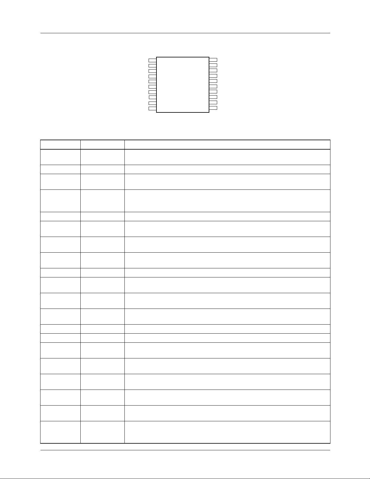
Pin Assignments
QCAP
PUMP
SDRAMOUT
SDRAMFB
5VSTBY
3VOUT1
3VOUT2
3VFB
PWRGD
SLP_S3#
1
2
3
4
5
6
7
8
9
10
RC5060
20
19
18
17
16
15
14
13
12
11
VCCP
5VOUT1
5VOUT2
5VFB
RAMBUSOUT
RAMBUSFB
GND
SS
PWROK
SLP_S5#
Pin Definitions
Pin Number Pin Name Pin Function Description
1 QCAP
2 PUMP
3 SDRAMOUT 3.3V SDRAM gate control. Attach this pin to a transistor powering 3.3V SDRAM
4 SDRAMFB
5 5VSTBY
6 3VOUT1
7 3VOUT2
8 3VFB
9 PWRGD
10 SLP_S3#
11 SLP_S5#
12 PWROK
13 SS
14 GND
15 RAMBUSFB
16 RAMBUSOUT 2.5V base drive control. Attach this pin to an NPN transistor powering 2.5V dual
17 5VFB
18 5VOUT2
19 5VOUT1
20 VCCP
Charge pump cap. Attach flying capacitor between this pin and PUMP to
generate high voltage from standby power.
Charge pump switcher.
from the 3.3V main supply.
3.3V SDRAM voltage feedback. Pin 4 is used as the input for the voltage
feedback control loop for 3.3V SDRAM, and also sources 3.3V SDRAM in
standby.
5V Standby. Apply +5V standby on this pin to run the circuit in standby mode.
3.3V main gate control. Attach this pin to a transistor powering 3.3V dual from
the 3.3V main supply.
3.3V standby gate control. Attach this pin to a transistor powering 3.3V dual
from the 5V standby supply.
3.3V voltage Feedback. Pin 8 is used as the input for the voltage feedback
control loop for 3.3V dual.
Power Good. Open collector output is high when all outputs are valid.
SLP_S3#. Control signal governing the Soft Off state S3. Internal current source
pulls this line high if left open.
SLP_S5#. Control signal governing the Soft Off state S5. Internal current source
pulls this line high if left open.
PWROK. Control signal for switches. Internal current source pulls this line high if left
open.
Softstart. Attach a capacitor to this pin to determine the softstart rate.
Ground. Connect this pin to ground.
2.5V feedback. Pin 15 is used as the input for the voltage feedback control loop for
2.5V dual (RAMBUS), and also sources 2.5V dual in standby.
(RAMBUS) from the 3.3V main supply.
5V Voltage Feedback. Pin 17 is used to sense undervoltage to protect the 5V dual
from overcurrent.
5V standby gate control. Attach this pin to a transistor powering 5V dual from the
5V standby supply.
5V main gate control. Attach this pin to a transistor powering 5V dual from the 5V
main supply.
Main Power. Apply +12V through a diode on this pin to run the circuit in normal
mode. Bypass with a 0.1µF capacitor. When 12V is not present, this pin produces
voltage doubled 5V standby.
REV. 1.0.2 9/14/01
Page 3
PRODUCT SPECIFICATION RC5060
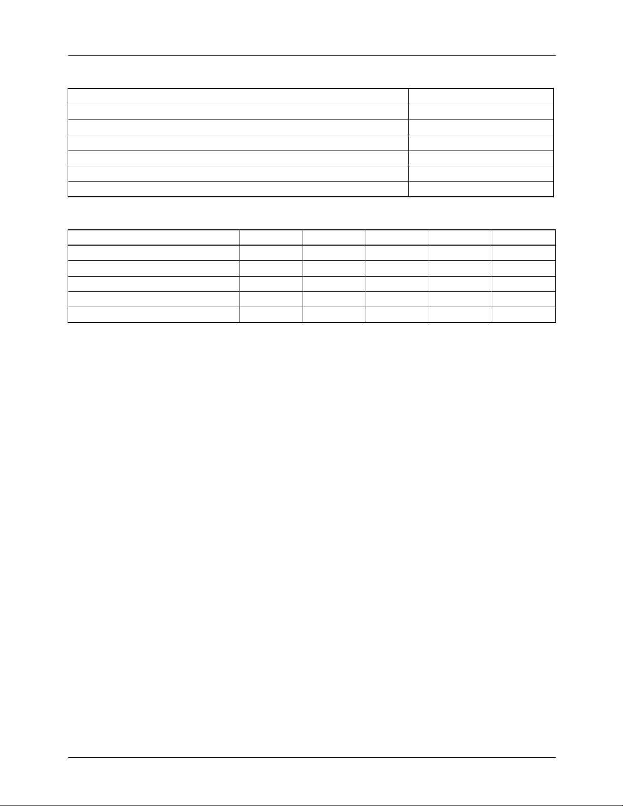
Absolute Maximum Ratings
VCCP 15V
All Other Pins 13.5V
Junction Temperature, T
J
150°C
Storage Temperature -65 to 150°C
Lead Soldering Temperature, 10 seconds 300°C
Thermal Resistance Junction to Ambient Θ
Thermal Resistance Junction-to-case, Θ
JC
JA
85°C/W
24°C/W
Recommended Operating Conditions
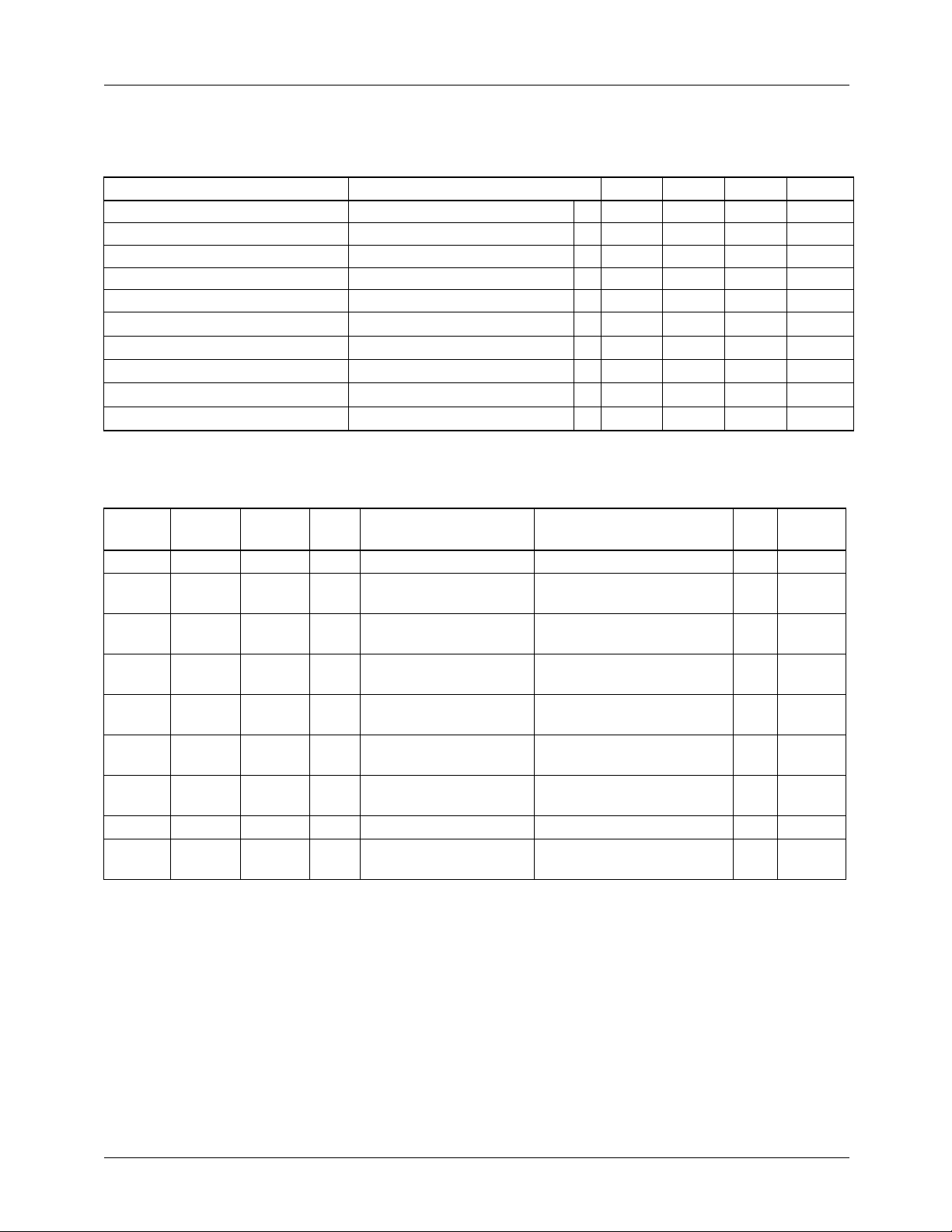
Parameter Conditions Min. Typ. Max. Units
+3.3VMAIN 3.135 3.3 3.465 V
+5VMAIN 4.75 5 5.25 V
+5VSTBY 4.75 5 5.25 V
+12V 11.4 12 12.6 V
Ambient Operating Temperature 0 70 °C
REV. 1.0.2 9/14/01
3
Page 4
4
RC5060 PRODUCT SPECIFICATION
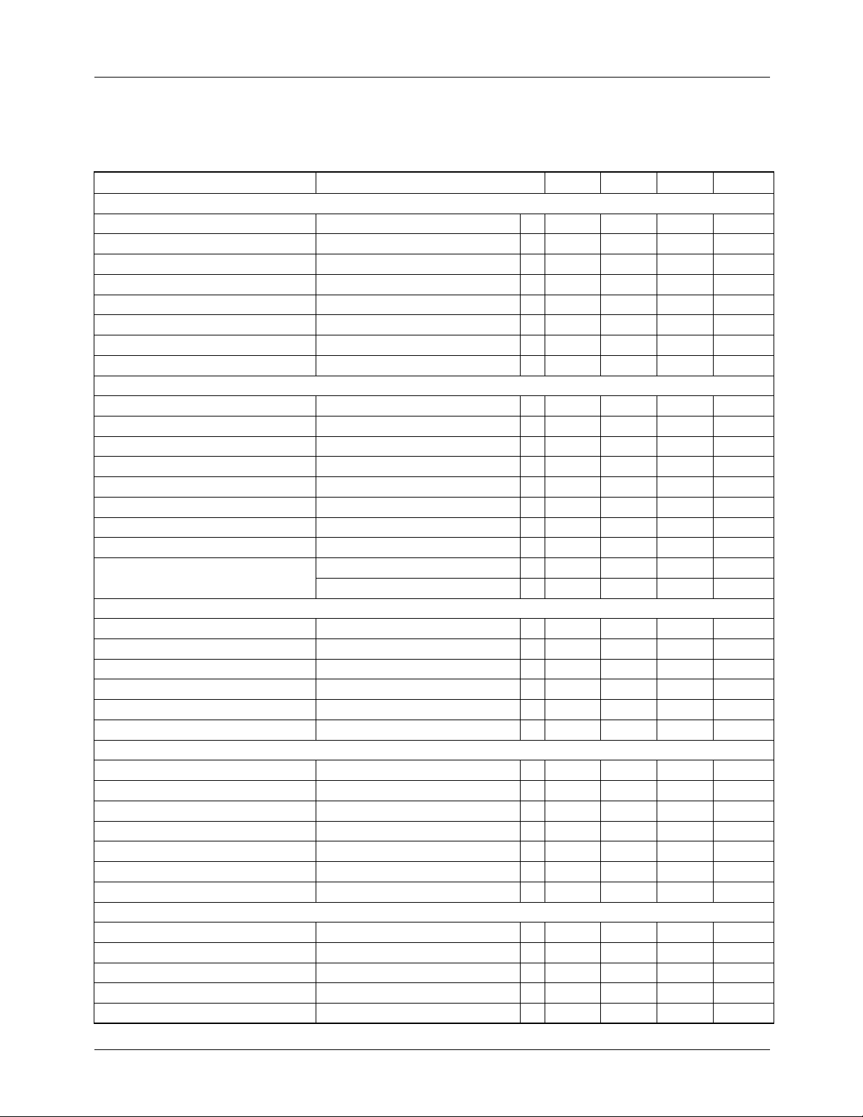
Electrical Specifications
(V
+5VSTBY
The • denotes specifications which apply over the full operating temperature range.
Parameter Conditions Min. Typ. Max. Units
+5V DUAL
V
Out1
V
Out1
V
GS
V
Out2
Maximum Drive Current, Each • 10 mA
Overcurrent Limit: Undervoltage 80 %V
Overcurrent Delay Time 150 µsec
Output Driver Overlap Time See Figure 2 • 1 5 µsec
+3.3V DUAL
V
Out1
V
Out1
V
Out2
Total Output Voltage Variation
Maximum Drive Current 3VOUT1 On • 90 mA
Minimum Load Current 3VOUT2 On • 50 mA
Overcurrent Limit: Undervoltage 80 %Vout
Overcurrent Delay Time 150 µsec
Output Driver Deadtime See Figure 2: Main → Standby • 2 6 µsec
+2.5V DUAL
I
B
I
Out
Total Output Voltage Variation
Overcurrent Limit 80 %Vout
Overcurrent Delay Time 150 µsec
Output Driver Overlap Time See Figure 2 • 1 5 µsec
+3.3V SDRAM
V
out
V
out
I
Out
Overcurrent Limit 80 %Vout
Total Output Voltage Variation
Overcurrent Delay Time 150 µsec
Output Driver Dead Time • 200 1500 nsec
Common Functions
PWRGD Threshold 80 %Vout
PWRGD Delay Time 150 µsec
PWRGD Sink Current • 1 mA
Charge Pump Frequency 250 KHz
+5VSTBY UVLO 4.5 V
= V
+5VMAIN
=5V, V
+3.3V
= 3.3V, V
= 12V and T
+12V
= +25°C using circuit in Figure 4, unless otherwise noted.)
A
, On • 10 V
, Off I = 10µA • 200 mV
,
Out2
Standby • 2.7 V
, Off I = 10µA • 200 mV
, On • 10 V
, Off I = 10µA • 200 mV
, On Standby • 5 mA
1
3VOUT2 On • 3.135 3.3 3.465 V
: Standby → Main • 200 1000 nsec
, On RAMBUSOUT On • 200 mA
RAMBUSOUT Off • 144 mA
1
• 2.375 2.5 2.625 V
, On • 10 V
, Off I = 10µA • 200 mV
SDRAMOUT Off • 100 mA
1
SDRAMFB On • 3.135 3.3 3.465 V
out
REV. 1.0.2 9/14/01
Page 5
PRODUCT SPECIFICATION RC5060
→
Electrical Specifications (continued)
(V
+5VSTBY
The • denotes specifications which apply over the full operating temperature range.
Parameter Conditions Min. Typ. Max. Units
+5VSTBY UVLO Hysteresis 0.5 V
+12V UVLO 7.5 V
+12V UVLO Hysteresis 1 V
+5VSTBY Current MAIN Power Present 10 25 mA
+12V Current 2.5 10 mA
Input Logic HIGH • 2.0 V
Input Logic LOW • 0.8 V
Softstart Current 3 6 9 µA
Control Line Input Current SLP_S5#, SLP_S3#, PWROK • 10 µA
Over Temperature Shutdown 150 °C
Note:
1. Voltage Regulation includes Initial Voltage Setpoint and Output Temperature Drift.
= V
+5VMAIN
=5V, V
+3.3V
= 3.3V, V
= 12V and T
+12V
= +25°C using circuit in Figure 4, unless otherwise noted.)
A
Table 1. Power Descriptors
2.5V RAMBUS/
PWROK SLP_S3# SLP_S5# Main 5V/3.3V Duals
1 1 1 ON ON, Powered from MAIN ON, Powered from MAIN S0 S0
1 0 1 OFF ON, Powered from
STANDBY
0 0 1 OFF ON, Powered from
STANDBY
0 1 1 OFF ON, Powered from
STANDBY
1 0 0 OFF ON, Powered from
STANDBY
0 0 0 OFF ON, Powered from
STANDBY
0 1 0 OFF ON, Powered from
STANDBY
1 1 0 ON ON, Powered from MAIN OFF S5 Not Used
000
1 OFF ON, Powered from
STANDBY
*When PWROK = SLP_S3# = 0 and SLP_S5# transitions from 0 to 1, the RC5060 remains in the S5 state. See Table 2.
3.3V SDRAM State Usage
ON, Powered from
S3 S0 → S3
STANDBY
ON, Powered from
S3 S3
STANDBY
ON, Powered from
S3 S3 → S0
STANDBY
OFF S5 S0 → S5
OFF S5 S5
OFF S5 S5 → S0
OFF S5* *
REV. 1.0.2 9/14/01
5
Page 6
6
RC5060 PRODUCT SPECIFICATION
101
111
S0
011
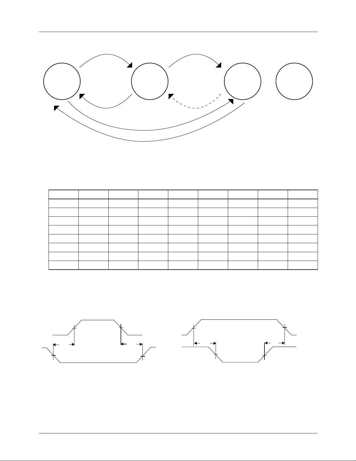
Table 2. State Transition Table
000 001 010 011 100 101 110 111
000
001
010
011
100
101
Initial Control Signal
110
111
—x-x—x—S0
S5 — S5 - S5 — S5 S0
—x-x—x—S0
S5 — S5 — S5 — S5 S0
—x—x—x—S0
S5 — S5 — S5 — S5 S0
—x—x—x—S0
S5 S3 S5 S3 S5 S3 S5 —
001
S3
Blocked
100
010
Figure 1. Power State Usage Diagram
Final Control Signal
000 110
S5
Not
Used
Notes:
1. Control Signal order: PWROK, SLP_S3#, SLP_S5#
2. Dash (—) signifies that no state change takes place.
3. X signifies that the state transition is blocked, and the RC5060 remains in the S5 state.
2V
t
DT
2V 2V
2V
t
DT
OUTPUT 1
OUTPUT2
2V
t
OT
2V
Figure 2. Deadtime and Overlap Time Measurements
2V
2V
t
OT
OUTPUT1
OUTPUT2
REV. 1.0.2 9/14/01
Page 7
PRODUCT SPECIFICATION RC5060
SLP_S3#
PWROK
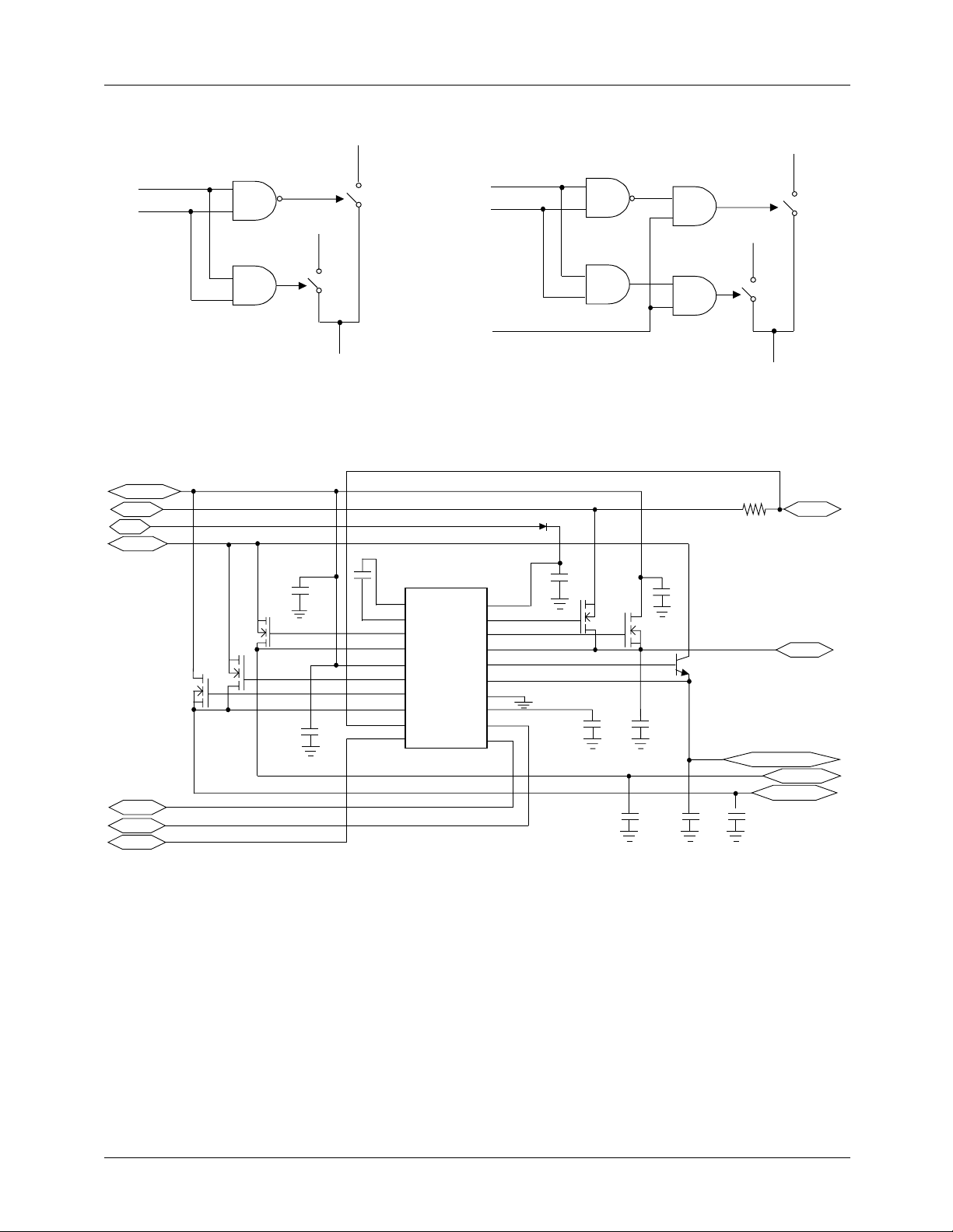
Figure 3. Control Logic for Dual Voltages and Memory Voltages
Application Circuits
+5V Standby
5V Main
+12V
3.3V Main
C3
Q1
Q3
Q4
SLP_S5#
PWROK
SLP_S3#
MAIN
C10
DUAL
STBY
C1
STBY
SLP_S3#
PWROK
MAIN
SLP_S5#
MEMORY
D1
C2
1
2
3
4
U1
5
RC5060
6
7
8
9
10
20
19
18
17
16
15
14
13
12
11
Q5
C7
C5
C9
Q6
Q2
C8
C6
R1
2.5V Dual (RAMBUS)
C4
PWRGD
+5V Dual
3.3V SDRAM
3.3V Dual (PCI)
REV. 1.0.2 9/14/01
Figure 4. Camino ACPI Selector
7
Page 8
PRODUCT SPECIFICATION RC5060
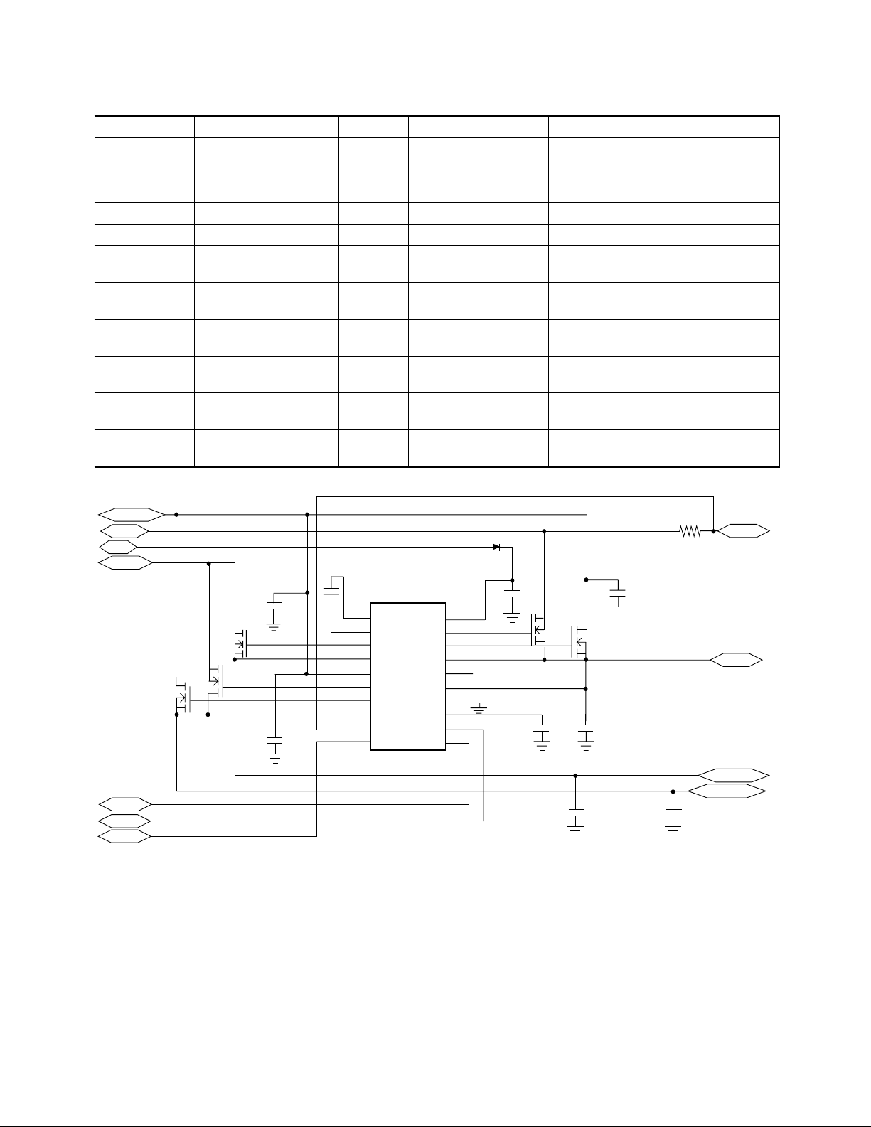
Table 3. RC5060 Application Bill of Materials for Camino
Reference Manufacturer, Part # Quantity Description Comments
C1-3, C8 Various 4 100nF, 25V Ceramic
C4–6, C9 Various 4 220µF, 6V Tantalum, ESR ~ 0.1 Ω
C7 Various 1 100nF, 50V Ceramic
C10 Various 1 47µF, 10V Tantalum
R1 Various 1 10K Ω Resistor
D1 Fairchild
MBR0520L
Q1, Q3 Fairchild
FDS4410DY
Q2 Fairchild
TIP41A
Q4 Fairchild
FDS6630A
Q5-6 Fairchild
NDH833N
U1 Fairchild
RC5060
1 20V, 1/2A Schottky
2 N-channel
MOSFET
1 NPN V
1 N-channel
MOSFET
2 N-channel
MOSFET
1 ACPI Switch
Controller
R
= 20m Ω @ V
ds,on
~0.4V @ I
CE
SO-8
R
= 25mΩ @ Vgs = 2.7V
ds,on
= 4.5V
gs
= 2A, IB = 100mA
C
+5V Standby
5V Main
+12V
3.3V Main
SLP_S5#
PWROK
SLPS3#
Q4
Q3
Q1
C3
C10
D1
C1
1
2
3
4
5
6
7
8
9
10
U1
RC5060
20
19
18
17
16
15
14
13
12
11
Figure 5. Whitney ACPI Selector
C2
Q5
C7
C5
R1
PWRGD
C9
Q6
+5V Dual
C8
3.3V SDRAM
3.3V Dual (PCI)
C4
REV. 1.0.2 9/14/01
8
Page 9
PRODUCT SPECIFICATION RC5060
Table 4. RC5060 Application Bill of Materials for Whitney
Reference Manufacturer, Part # Quantity Description Comments
C1-3, C8 Various 4 100nF, 25V Ceramic
C4-5, C9 Various 3 220µF, 6V Tantalum, ESR ~ 0.1Ω
C7 Various 1 100nF, 50V Ceramic
C10 Various 1 47µF, 10V Tantalum
R1 Various 1 10KΩ Resistor
D1 Fairchild
MBR0520L
Q1, Q3 Fairchild
FDS4410DY
Q4 Fairchild
FDS6630A
Q5-6 Fairchild
NDH833N
U1 Fairchild
RC5060
1 20V, 1/2A Schottky
2 N-channel
MOSFET
1 N-channel
MOSFET
2 N-channel
MOSFET
1 ACPI Switch
Controller
R
= 20mΩ @ Vgs = 4.5V
ds,on
SO-8
= 25mΩ @ Vgs = 2.7V
R
ds,on
ATX
5Vmain, 18A
5Vstdby 720mA
12V, 6A
3.3Vmain, 14A
Switch Switch
RC5060
SO20
PWROK SLP_S3# SLP_S5#
Typedet
Linear
RC5058
Switch
SO24
RC1587
Linear
Linear
Vcore 2V/17.4A
Synchronous
Conversion
Vnb 1.8V/2A
Linear
Linear/Switch
Linear
5Vdual 1A/1A/200mA USB
3.3Vdual 2.4A/500mA/500mA PCI
Vagp 3.3V/1.5V/2A
Vck 2.5V/600mA
2.5V RAMBUS @ 2A/144mA
Vtt 1.5V/2A
Linear
Switch
3.3V SDRAM @ 4.8A/100mA
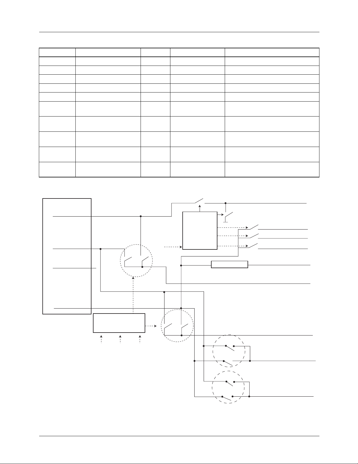
Figure 6. Camino System Architectural Block Diagram (Power Paths Only)
REV. 1.0.2 9/14/01 9
Page 10

RC5060 PRODUCT SPECIFICATION
Application Information
The RC5060 Controller
The RC5060 is a fully compliant ACPI controller IC. Used
with an ATX power supply, it generates a 5V Dual voltage, a
3.3V Dual for PCI, and power for both SDRAM and RAMBUS, and has a large array of additional protection functions
integrated in. Used in conjunction with Fairchild’s RC5058,
it provides the complete set of control and power functions
necessary to implement a Camino or Whitney motherboard.
It can also be used to generate the dual voltages necessary for
a Tehama motherboard.
Overview of ACPI
The Advanced Configuration and Power Interface, or ACPI,
is a system for controlling the use of power in a computer. It
enables the computer manufacturer and the computer user to
determine the computer’s power usage dynamically. For
example, when the computer has been unused for a certain
time, the monitor and peripherals could be turned off, and
their states saved to memory. After a longer period, the
processor could be turned off, and the memory saved to disk.
A peripheral could then re-awaken the entire system on the
occurrence of an event, such as the arrival of a FAX on a
modem.
As shown in Figure 6, the available power inputs to the computer system from the ATX power supply are +5V main, +12V
main, +3.3V main, and +5V standby. “Main” means that
these power outputs are available under full-power operation
of the system, but can be turned off in some of the powersaving modes. “Standby” means that this power output is
always present.
The most general ACPI system requires four dual outputs:
5V dual, 3.3V dual, 3.3V SDRAM, and 2.5V RAMBUS (or
2.5V dual). “Dual” means that the power can be (but is not
necessarily) present whether the main power supplies are
present or not. To ensure the presence of these outputs, while
not overloading the standby power, they have dual inputs,
from both main power and standby. The presence or absence
of the dual outputs is determined by the control signals to the
RC5060.
ACPI States
As shown in Table 1, there are three ACPI states that are of
primary concern to the system designer, designated S0, S3
and S5. S0 is the full-power state, the state of the computer
when it is being actively used. The other two states are sleep
states, reflecting differing levels of power-down.
S5 is a state in which memory is off, and the last state of the
processor has been written to the hard disk. Since the disk is
slow, the computer takes longer to come back to full operation.
However, since memory is off, this state draws minimal
power.
It is anticipated that only the following state transitions will
occur: S0 → S3, S0 → S5, S3 → S5, S5 → S0, and S3 → S0;
the transition S5 → S3 will occur only as an intermediate state
during the transition from S5 → S0. To prevent overcurrent
limit from activating, the RC5060 blocks this transition. For
example, when PWROK = SLP_S3# = 0, and SLP_S5# transitions from 0 to 1, the RC5060 remains in the S5 state. See
Table 2.
5V Dual Output
The RC5060 controls four separate dual outputs, the first of
which is the 5V dual. This output is intended to run subsystems such as the USB ports. A typical application that
would require the use of 5V dual rather than +5V main for a
USB port would be the use of a USB mouse: if the system
needs to be able to awaken from sleep when the mouse is
moved, then the mouse must be powered from dual, because
main power is off.
5V dual is generated by two MOSFET switches, one from
+5V main, the other from +5V standby, as shown in Figures
4 or 5. When main power is present, the first switch is on and
the second off, and the opposite when main power is absent.
Note carefully the polarity of the MOSFET Q5 that delivers
power from the +5V main to the 5V dual: opposite to the
connection of Q6, the source is connected to the +5V main
input, and the drain is connected to the 5V dual output. This
connection must be done this way because of Q5’s body
diode. When +5V main is not present, 5V dual is still on, and
if Q5 were connected with the same polarity as Q6, the dual
voltage would conduct through the body diode of Q5,
attempting to power up the entire +5V main line. It is to
avoid this overload that Q5 must be connected as shown.
The state of the switches is controlled by the SLP_ S3# and
PWROK lines, as shown in Figure 3. When both SLP_ S3#
and PWROK are asserted, the main switch is on, and the
standby switch is off. If either line is de-asserted, the main
switch is off and the standby switch is on.
Note that Q5 and Q6 should be low-gate-voltage type
MOSFETs, with guaranteed operation at 2.7V Vgs, in order
to ensure full enhancement in worst case. In a typical system,
it is anticipated that full-power current will be about 1A maximum, and standby current will be about 200mA maximum.
S3 is a state in which the processor is powered down, but its
last state is being preserved in IC memory, which is kept on.
Since memory is fast, the computer can quickly come back
up to full operation. However, this state continues to draw
moderate power, due to the memory being kept alive.
10 REV. 1.0.2 9/14/01
3.3V Dual Output
The 3.3V dual output is intended to power subsystems such
as the computer’s PCI slots. A typical application that would
require the use of 3.3V dual rather than +3.3V main for a PCI
slot would be the use of a modem: if the system needs to be
Page 11
PRODUCT SPECIFICATION RC5060
able to awaken from sleep when the modem receives incoming data, then that slot must be powered from dual, because
main power is off. Other slots not requiring dual power can
be configured using the control signals.
3.3V dual is generated by two MOSFETs, one from +3.3V
main, the other from +5V standby, as shown in Figures 4 or
5. When main power is present, the MOSFET Q3 is turned
on as a switch, so that input and output are connected
together. When main power is absent, the MOSFET Q4 is
controlled by the RC5060 as a linear regulator, generating a
regulated 3.3V from +5V standby. As with the 5V dual, the
MOSFET Q3 must
be connected as shown in the figures, to
avoid back-feed.
The state of the MOSFETs is controlled by the SLP_S3# and
PWROK lines, as shown in Figure 3. When both SLP_S3#
and PWROK are asserted, the main switch is on, and the linear
regulator is off. If either line is de-asserted, the main switch
is off and the linear regulator is on.
Q3 and Q4 as shown in Tables 3 or 4 have different R
DS,on
ratings. In a typical system, it is anticipated that full-power
current will be about 2.4A maximum, and standby current
will be about 500mA maximum. The difference in maximum
currents means that Q4 can be a less expensive device than Q3.
The design of the linear regulator for the 3.3V Dual necessitates a minimum load current of 50mA. Furthermore, in
order to guarantee stable operation, the output capacitor on
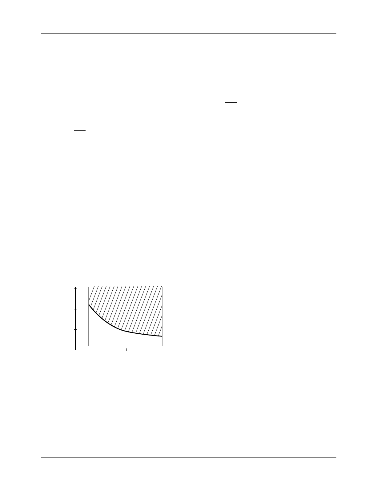
the 3.3V Dual must have a minimum ESR as shown in Figure 7. The hatched region shows acceptable values of ESR
vs. output capacitance. Values of the output capacitor less
than 47µF or greater than 300µF are not recommended.
300
200
ESR (mΩ)
100
47 330100 200
C (µF)
Figure 7. Recommended C vs. ESR for
Stable Operation of the 3.3V Dual
300 400
3.3V SDRAM is generated by one external MOSFET switch
from +3.3V main, and one linear regulator internal to the
RC5060 from +5V standby, as shown in Figures 4 or 5, and
in the block diagram on the front page. When main power is
present, the MOSFET Ql is turned on as a switch, so that
input and output are connected together. When main power
is absent, the internal linear regulator is on, generating a regulated 3.3V from +5V standby. As with the other duals, the
MOSFET Ql must be connected as shown in the figures, to
avoid back-feed.
The state of the external MOSFET and the internal linear
regulator is controlled by the SLP_S3# and PWROK lines,
and additionally the SLP_S5# line, as shown in Figure 3.
When SLP_S5# is de-asserted, both the external MOSFET
and the internal linear regulator are off, and there is no output voltage on the 3.3V SDRAM line.
If the SLP_S5# line is asserted, the 3.3V SDRAM output is
on. In this condition, if either the SLP_S3# or the PWROK
line, or both, are de-asserted, the linear regulator is on and
the MOSFET is off. Only in the case if both the SLP_S3#
and the PWROK lines are asserted, the MOSFET is on and
the linear regulator is off.
In a typical system, it is anticipated that standby current will
be about 100mA maximum. Full power current will be as
high as 4.8A maximum, so that Ql must have a low R
DS,on
in order to prevent excessive voltage drop across it.
2.5V Dual Output
The 2.5V dual output is intended to provide power to RAMBUS memory. Only high-end systems will use this power.
Those systems using RAMBUS may also use the SDRAM
power, possibly piped to the same slots, to ensure backward
compatibility or even mixed operation of SDRAM with
RAMBUS.
2.5V dual is generated by one external NPN bipolar acting as
a linear regulator from +3.3V main, and one linear regulator
internal to the RC5060 from +5V standby, as shown in Figure 4, and in the block diagram on the front page. When
main power is present, the NPN Q2 linear regulates, and
when main power is absent, the internal linear regulator is
on. Q2 cannot be substituted with a MOSFET. If used in one
direction, the MOSFET’s body diode would permit backfeed; if used in the other direction, it would short-circuit the
linear regulator action.
3.3V SDRAM Output
3.3V SDRAM output is intended to provide power to
SDRAM memory. Most systems will use this power. Those
systems using RAMBUS may also use the SDRAM power,
possibly piped to the same slots, to ensure backward compatibility or even mixed operation of SDRAM with RAMBUS.
REV. 1.0.2 9/14/01 11
2.5V dual output is controlled in the same way and by the
same lines as the 3.3V SDRAM output. In a typical system,
it is anticipated that standby current will be a maximum of
144mA, and full-power current may be as high as 2A. This
places some significant constraints on the selection of Q2.
Since its input may be as low as (3.3V - 5%) = 3.135V, there
is only 3.135V -2.5V = 635mV of V
headroom for its
CE
Page 12

RC5060 PRODUCT SPECIFICATION
operation as a linear regulator. For this reason the RC5060
can provide up to 200mA of steady-state base current. The
TIP41A device shown has a sufficiently low V
tee worst-case regulation even at 2A IE with this base current.
CE, sat
to guaran-
RC5060 ACPI Control Lines
As already discussed, the RC5060 outputs are controlled by
the three ACPI control lines, SLP_S3#, SLP_S5# and
PWROK, as summarized in Tables 1 and 2. System designers must in particular be careful to ensure that their system is
designed with SLP_S5#, not SLP_S5; if SLP_S5 is used, it
must be inverted before being used with the RC5060.
The control lines have internal pull-ups of approximately
10µA, and so can be controlled by open collector drivers if
desired. In a noisy system, it may be desirable to filter these
lines, which can be done with a 1KΩ resistor and a small
capacitor.
RC5060 Dynamic Operation
The RC5060 is designed to minimize the output capacitance
required to hold up the various output lines during transitions
between different states. Thus in particular, the 5V dual and
2.5V dual outputs have guaranteed minimum overlap times,
the time (as shown in Figure 2) during a state transition during which both main and standby are connected to the output. This overlap time guarantees that a power source is
always connected to the output, so that there will be no dip in
the output voltage during state transitions. There is also a
maximum overlap time, to ensure that the standby power
doesn’t have to source main power very long, thus minimizing thermal stress on the standby device.
The 3.3V dual and 3.3V SDRAM are different than the other
outputs, because they are powered by both a linear regulator
and a switch. If the linear regulator were to turn on while the
switch is on (or vice versa) the linear regulator would supply
power to the main line through the switch. For this reason,
the linear regulator must be off before the switch is on, and
vice versa. Thus, these two outputs have guaranteed minimum
deadtime when both linear regulator and switch are off. During this time, the output capacitors must hold up the load,
and so there is also a specified maximum deadtime, allowing
a maximum necessary capacitance to be selected, see below.
Stability
As with all linear regulators, the RC5060’s linear regulators
require a minimum load. With the exception of the 3.3V dual
output, however, all of these minimum loads are internal to
the RC5060. The 3.3V dual output requires a minimum load
of 50mA; if a situation may occur in which the load is less than
50mA, additional steps may be necessary to ensure stability.
Furthermore, depending on location, it may be necessary to
bypass the drain (or collector) of the linear regulator with a
low ESR capacitor for stability. As a rule of thumb, if the
pass element is more than 1” from its power source, it should
have a bypass.
Softstart
Pin 13 of the RC5060 functions as a softstart. When power is
first applied to the chip, a constant current is applied from
the pin into an external capacitor, linearly ramping up the
voltage. This ramp in turn controls the internal reference of
the RC5060. providing a softstart for the linear regulators.
The actual state of the RC5060 on power up will be determined by the state of its control lines.
The switches in the system must be either on or off, and so
softstart has no effect on their characteristics: if the appropriate control signals are asserted, they will turn on at once.
The softstart is effective only during power on. During a
transition between states, such as from S5 → S0, the linear
regulators are not softstarted.
It is important to note that the softstart pin is not
pulling it low will not necessarily turn off all outputs.
an enable;
Charge Pump
In main power operation, the RC5060 is run from the +12V
main supply. This supply also provides voltage to the various
MOSFET gates. However, during standby, this supply is off.
To provide power to the chip and the appropriate gates, the
RC5060 incorporates a free-running charge pump. As shown
in Figures 4 and 5, and in the block diagram on the front
page, a capacitor attached between pins 1 and 2 of the RC5060
acts as a charge pump with internal diodes. The charge pump
output is internally diode or’red with the 12V input. The 12V
input must have a series diode to prevent back-feeding the
charge pump to the + 12V main when in standby. The 12V
input line needs a bypass capacitor for high-frequency noise
rejection.
Overcurrent
The RC5060 does not directly detect current through the
eight devices that power its outputs. Instead, it monitors the
four output voltages. In the event of a hard short, the voltage
drops below 80% of nominal, and all outputs are latched off,
and remain off until 5V standby power is recycled. The overcurrent latch off is delayed by 150µsec to prevent nuisance trips.
In the S5 state, when the memory outputs are off, the voltage
monitors on the memory lines are disabled, to prevent tripping the overcurrent. When turning these lines back on from
the S5 state, overcurrent is prevented from tripping because
the S3 state is blocked. See Table 2.
If the 2.5V dual is not used, its feedback line, pin 15, must be
connected to 5V dual as shown in Figure 5, to prevent an
overcurrent trip.
UVLO
If the +5V standby is below approximately 4.5V, the RC5060
will leave off or turn off all outputs. Similar comments apply
to the +12V main at 7.5V. The +5V standby UVLO has
approximately 0.5V hysteresis, the +12V main UVLO 1V.
12 REV. 1.0.2 9/14/01
Page 13
PRODUCT SPECIFICATION RC5060
Power Good
The Power Good is an open collector that pulls low if any of
the outputs are less than 80% of nominal.
Over Temperature
The RC5060 is capable of sourcing substantial current, 200mA
minimum to the RAMBUS transistor’s base during S0, 144mA
to the RAMBUS line during S3, and 100mA to SDRAM
during S3. As a result, there can be heavy power dissipation
in the IC. While the RC5060 is designed to accept this power
dissipation, any overloading of outputs can cause excessive
heating. If the RC5060 die temperature exceeds about 150°,
all outputs are shut off. Outputs remain off until the die
temperature returns to its safe area.
Transistor Selection
External transistor selection depends on usage, differing for
the linear regulators and the switches.
The MOSFET switches, Ql, Q3, Q5 and Q6 should be sized
based on regulation requirements and power dissipation.
Since the ATX outputs are ±5%, the outputs driven from
them must be wider. As an example, if we want to hold 3.3V
SDRAM to -10%, we can drop only 5% = 165mV across Q1.
At 4.8A, this means Ql must have a maximum R
165mV/4.8A = 34mΩ, including tolerance and self-heating
effects. We thus choose a Fairchild FDS4410Y, which has
20mΩ maximum R
at 4.5V VGS at 25°C. We can esti-
DS, on
mate power dissipation as (4.8A)2 * 20mΩ = 460mW, which
should be acceptable for this package. Similar calculations
apply to the other MOSFET switches.
Q4 is a MOSFET functioning as a linear regulator. Since it
delivers only 500mA, it is easy to select a MOSFET, it need
only be able to handle 500mA * (5V±5%–3.3V) = 1W. We
select the Fairchild FDS6630A in an SO-8 package.
DS,on
of
Alternate for 2.5V Dual
I
nstead of the bipolar transistor shown in Figure 4 for Q2, the
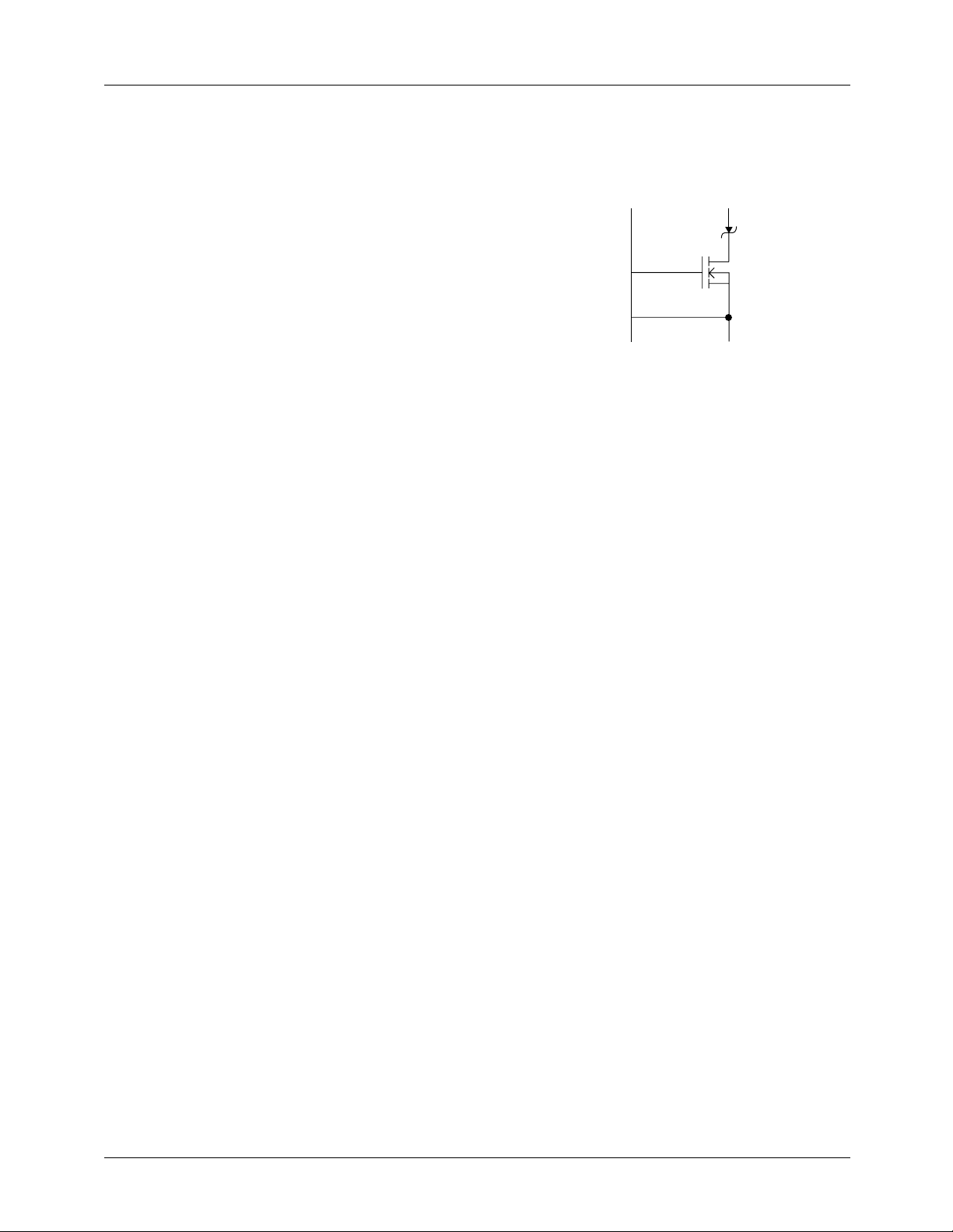
linear pass element for the 2.5V dual for RAMBUS, a MOSFET and schottky diode can be used as shown in Figure 8.
3.3V Main
RC5060
Figure 8. 2.5V Dual with MOSFET
16
15
2.5V Dual
(RAMBUS)
The schottky should be chosen to have a low Vf at the specified RAMBUS current. The MOSFET’s R
lower than (3.3V—5% -2.5V - Vf)/I
RAMBUS
must then be
DS,on
including temperature. An additional constraint is that the MOSFET must
have a gate threshold voltage lower than 1.5V. For example, for
2.8A, choose the diode to be an MBR835, and the MOSFET a
Fairchild NDH833N. This same technique can then also be
used for RAMBUS currents higher than can be achieved
with the bipolar transistor.
Output Capacitor Selection
Output capacitor selection depends on whether the line has
overlap time or not.
For both the 5V dual and the 2.5V dual, there is guaranteed
overlap time between when one source is turned on and the
other source turned off. For these outputs, the output capacitor is not needed to hold up the supply, but only for noise
filtering and to respond to transient loading.
Q2 is an NPN bipolar functioning as a linear regulator. As
already discussed, it must have a V
lower than 635mV
CE,sat
at IE = 2A and IB = 200mA. Its power dissipation can be as
high as (3.3V + 5%–2.5V) * 2A = l.9W.
The 3.3V dual and 3.3V SDRAM outputs have deadtime
between when one source is turned off and the other source
turned on. During the time when both are off, the output current must be supplied by the output capacitor. Mitigating
this, it must be realized that the system will be designed in
such a way that the current has gone to its sleep value before
the transition occurs. For example, the 3.3V dual has a sleep
current of 500mA maximum. Maximum deadtime is 6µsec,
and so charge depletion is 500mA * 6µsec = 3µC. Suppose
that we have a total of 8% drop due to the source tolerance
and the MOSFET drop, and we are trying to hold 10%
regulation. The remaining 2% = 66mV implies a minimum
capacitance of 3µC/66mV = 45µF.
REV. 1.0.2 9/14/01 13
Page 14
PRODUCT SPECIFICATION RC5060
Mechanical Dimensions
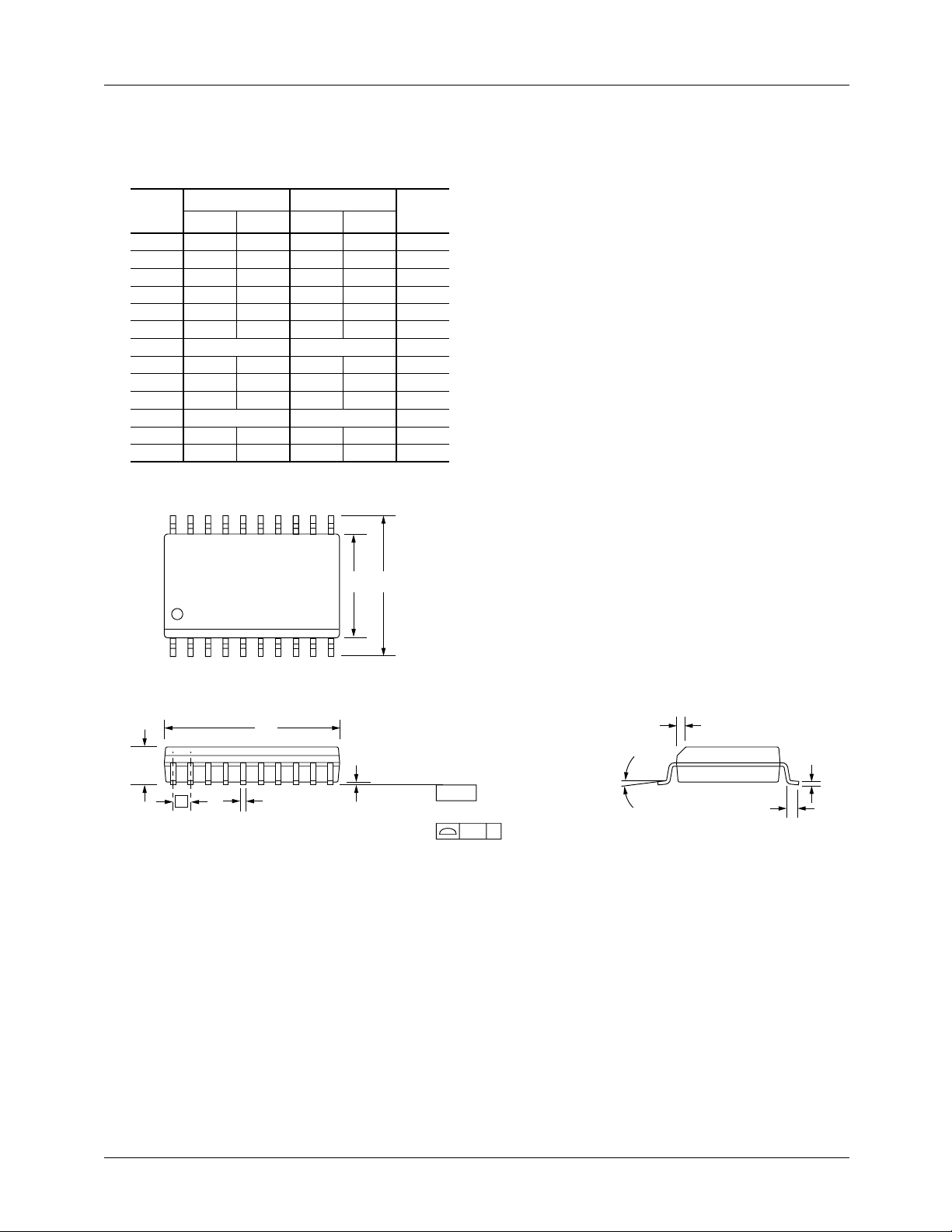
20 Lead SOIC
Symbol
A .093 .104 2.35 2.65
A1 .004 .012 0.10 0.30
B .013 0.33
C .009 .013 0.23 0.32
D .496 .512 12.60 13.00
E .291 .299 7.40 7.60
e
H
h
L .016 .050 0.40 1.27
N20 20
α
ccc .004 0.10——
20
Inches
Min. Max. Min. Max.
.020 0.51
.050 BSC 1.27 BSC
.394 .419 10.00 10.65
.010 .029 0.25 0.75
0° 8° 0° 8°
Millimeters
11
EH
Notes
5
2
2
3
6
Notes:
1.
Dimensioning and tolerancing per ANSI Y14.5M-1982.
2.
"D" and "E" do not include mold flash. Mold flash or
protrusions shall not exceed .010 inch (0.25mm).
3.
"L" is the length of terminal for soldering to a substrate.
4.
Terminal numbers are shown for reference only.
5.
"C" dimension does not include solder finish thickness.
6.
Symbol "N" is the maximum number of terminals.
1
D
A
e
B
10
A1
SEATING
PLANE
– C –
LEAD COPLANARITY
ccc C
h x 45°
C
α
L
REV. 1.0.2 9/14/01 14
Page 15
RC5060 PRODUCT SPECIFICATION
Ordering Information
Product Number Package
RC5060M 20 pin SOIC
DISCLAIMER
FAIRCHILD SEMICONDUCTOR RESERVES THE RIGHT TO MAKE CHANGES WITHOUT FURTHER NOTICE TO ANY
PRODUCTS HEREIN TO IMPROVE RELIABILITY, FUNCTION OR DESIGN. FAIRCHILD DOES NOT ASSUME ANY
LIABILITY ARISING OUT OF THE APPLICATION OR USE OF ANY PRODUCT OR CIRCUIT DESCRIBED HEREIN; NEITHER
DOES IT CONVEY ANY LICENSE UNDER ITS PATENT RIGHTS, NOR THE RIGHTS OF OTHERS.
LIFE SUPPORT POLICY
FAIRCHILD’S PRODUCTS ARE NOT AUTHORIZED FOR USE AS CRITICAL COMPONENTS IN LIFE SUPPORT DEVICES
OR SYSTEMS WITHOUT THE EXPRESS WRITTEN APPROVAL OF THE PRESIDENT OF FAIRCHILD SEMICONDUCTOR
CORPORATION. As used herein:
1. Life support devices or systems are devices or systems
which, (a) are intended for surgical implant into the body,
or (b) support or sustain life, or (c) whose failure to perform
when properly used in accordance with instructions for use
2. A critical component is any component of a life support
device or system whose failure to perform can be
reasonably expected to cause the failure of the life support
device or system, or to affect its safety or effectiveness.
provided in the labeling, can be reasonably expected to
result in significant injury to the user.
www.fairchildsemi.com
9/14/01 0.0m 003
2000 Fairchild Semiconductor Corporation
Stock#DS30005060
 Loading...