

Page 1
www.fairchildsemi.com
RC1584
7A Adjustable/Fixed Low Dropout Linear Regulator
Features
• Fast transient response
• Low dropout voltage at up to 7A
• Load regulation: 0.05% typical
• Trimmed current limit
• On-chip thermal limiting
• Standard TO-220, TO-263 and TO-263 center cut
packages
Applications
• Pentium® Class GTL+ bus supply
• Low voltage logic supply
• Post regulator for switching supply
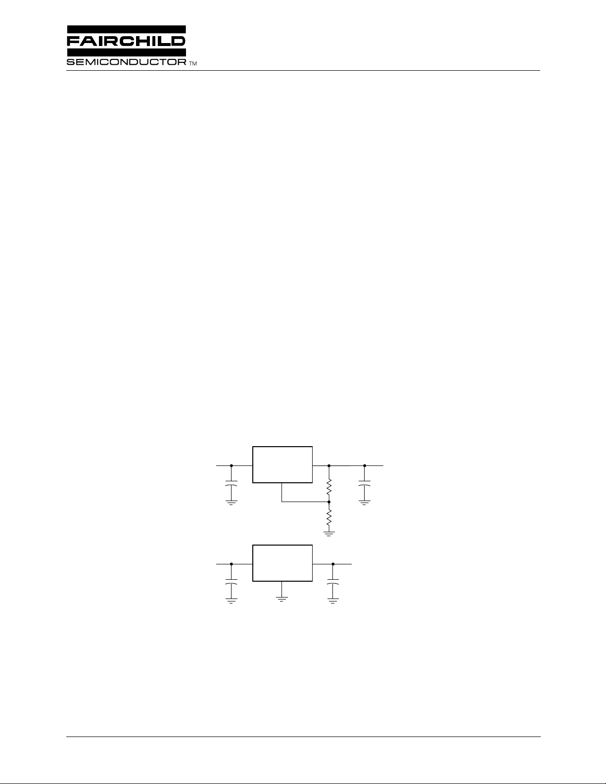
Typical Applications
= 3.3V
V
IN
+
10µF
V
IN
RC1584
ADJ
Description
The RC1584 and RC1584-1.5 are low dropout three-terminal
regulators with 7A output current capability . These devices
have been optimized for low voltage applications including
VTT bus termination, where transient response and minimum
input voltage are critical. The RC1584 is ideal for low
voltage microprocessor applications requiring a regulated
output from 1.5V to 3.6V with an input supply of 5V or less.
The RC1584-1.5 offers fixed 1.5V with 7A current capability for GTL+ bus V
Current limit is trimmed to ensure specified output current
and controlled short-circuit current. On-chip thermal limiting
provides protection against any combination of overload and
ambient temperature that would create excessive junction
temperatures.
The RC1584 and RC1584-1.5 are available in the industrystandard TO-220, TO-263 and TO-263 center cut power
packages.
V
OUT
124Ω
+
TT
22µF
termination.
1.5V at 7A
= 3.3V
V
IN
10µF
Pentium is a registered trademark of Intel Corporation.
+
RC1584-1.5
V
IN
GND
V
OUT
24.9Ω
+
22µF
1.5V at 7A
65-1584-16
REV. 1.0.5 7/13/00
Page 2
RC1584 PRODUCT SPECIFICATION
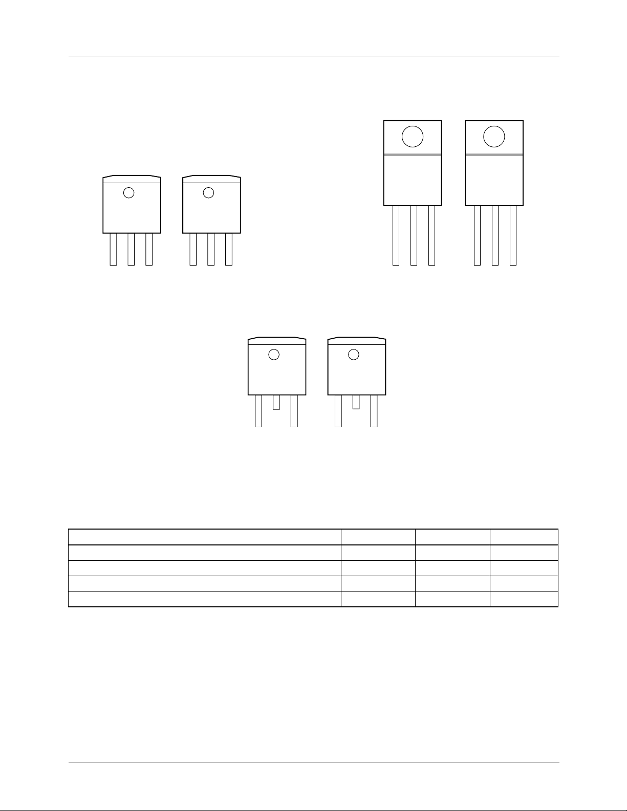
Pin Assignments
RC1584T-1.5RC1584T
FRONT VIEW
FRONT VIEW
RC1584MRC1584M-1.5
FRONT VIEW
FRONT VIEW
123
123
GND OUT
IN
3-Lead Plastic TO-263
θJC = 3°C/W*
* θJA can vary from 20°C/W to >40°C/W with various mounting techniques.
123
IN
RC1584MCRC1584MC-1.5
FRONT VIEW
123
GND
3-Lead Plastic TO-263 Center Cut
IN
θJC = 3°C/W*
FRONT VIEW
123
ADJ
IN
ADJ
OUT
INADJ OUT
3-Lead Plastic TO-220
θJC = 3°C/W
Tab is Out.
123
GND OUT
65-1584-02
IN
Absolute Maximum Ratings
Parameter Min. Max. Unit
V
IN
Operating Junction Temperature Range 0 125 °C
Storage Temperature Range -65 150 °C
Lead Temperature (Soldering, 10 sec.) 300 °C
2 REV. 1.0.5 7/13/00
7V
Page 3

PRODUCT SPECIFICATION RC1584
Electrical Characteristics
Tj = 25°C unless otherwise specified.
The • denotes specifications which apply over the specified operating temperature range.
Parameter Conditions Min. Typ. Max Units
Reference Voltage
Output Voltage
Line Regulation
Load Regulation
3
4
1, 2
1, 2
Dropout Voltage ∆V
Current Limit (VIN – V
Adjust Pin Current
3
Adjust Pin Current Change31.5V ≤ (VIN – V
Minimum Load Current 1.5V ≤ (VIN – V
Quiescent Current VIN = 5V • 413mA
Ripple Rejection f = 120Hz, C
Thermal Regulation TA = 25°C, 30ms pulse 0.004 0.02 %/W
Temperature Stability • 0.5 %
Long-Term Stability TA = 125°C, 1000 hrs. 0.03 1.0 %
RMS Output Noise
(% of V
OUT
)
Thermal Resistance,
Junction to Case
Thermal Shutdown 150 °C
Notes:
1. See thermal regulation specifications for changes in output voltage due to heating effects. Load and line regulation are
measured at a constant junction temperature by low duty cycle pulse testing.
2. Line and load regulation are guaranteed up to the maximum power dissipation (18W). Power dissipation is determined by
input/output differential and the output currrent. Guaranteed maximum output power will not be available over the full input/
output voltage range.
3. RC1584 only.
4. RC1584-1.5 only.
1.5V ≤ (VIN – V
10mA ≤ I
OUT
3.3V ≤ VIN ≤ 7V
10mA ≤ I
(V
I
OUT
(VIN – V
10mA ≤ I
OUT
+ 1.5V) ≤ VIN ≤ 7V,
OUT
= 10mA
) = 3V
OUT
OUT
= 1%, I
REF
) = 2V • 7.1 8 A
OUT
OUT
≤ 7A
) ≤ 5.75V,
• 1.225
(-2%)
1.250 1.275
(+2%)
• 1.47 1.5 1.53 V
≤ 7A
• 0.005 0.2 %
• 0.05 0.5 %
≤ 7A
= 7A • 1.150 1.300 V
OUT
V
• 35 120 µA
10mA ≤ I
(VIN – V
OUT
OUT
) ≤ 5.75V,
OUT
≤ 7A
) ≤ 5.75V • 10 mA
OUT
= 22µF Tantalum,
OUT
) = 3V, I
OUT
= 7A
• 0.2 5 µA
60 72 dB
TA = 25°C, 10Hz ≤ f ≤ 10kHz 0.003 %
TO-220 3 °C/W
TO-263 3 °C/W
REV. 1.0.5 7/13/00 3
Page 4
RC1584 PRODUCT SPECIFICATION
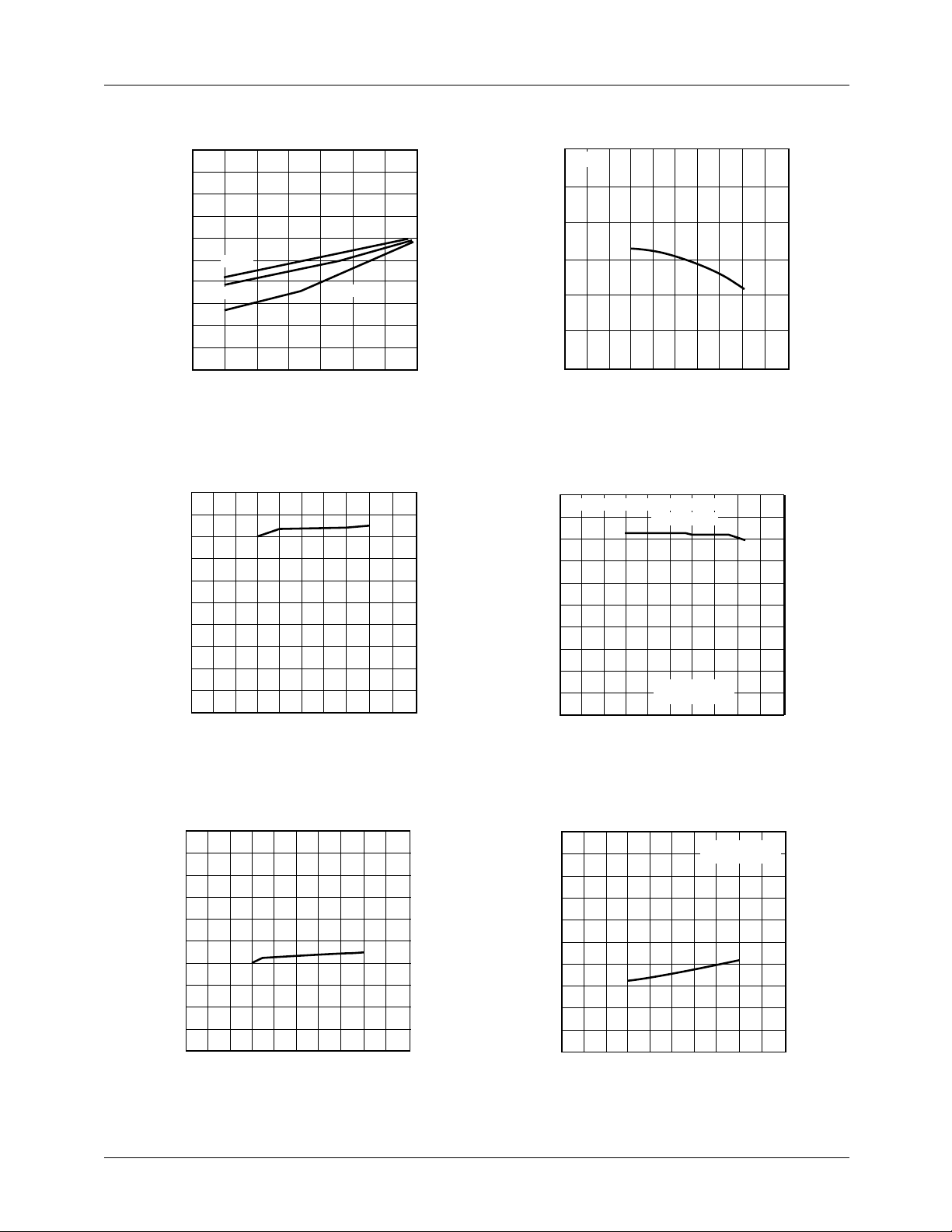
Typical Performance Characteristics
1.5
1.4
1.3
1.2
1.1
1.0
0.9
0.8
DROPOUT VOLTAGE (V)
0.7
0.6
0.5
T=0°C
T=25°C
123
OUTPUT CURRENT (A)
T=125°C
65-1584-03
54760
0.10
∆I = 7A
0.05
0
-0.05
-0.10
-0.15
OUTPUT VOLTAGE DEVIATION (%)
-0.20
-75 -50 -25 0 25 50 75 100 125 150 175
JUNCTION TEMPERATURE (°C)
65-1584-04
Figure 1. Dropout Voltage vs. Output Current Figure 2. Load Regulation vs. Temperature
1.275
1.270
1.265
1.260
1.255
1.250
1.245
1.240
REFERENCE VOLTAGE (V)
1.235
1.230
1.225
-75 -50 -25 0 25 50 75 100 125 150 175
JUNCTION TEMPERATURE (°C)
65-1584-05
3.70
V
SET WITH 1% RESISTORS
OUT
3.65
3.60
3.55
3.50
3.45
3.40
3.35
REFERENCE VOLTAGE (V)
3.30
3.25
3.20
-75 -50 -25 0 25 50 75 100 125 150 175
JUNCTION TEMPERATURE (°C)
V
= 3.6V
OUT
Note:
1. RC1584 Only
1
65-1584-06
Figure 3. Reference Voltage vs. Temperature Figure 4. Output Voltage vs. Temperature
5
4
3
2
1
MINIMUM LOAD CURRENT (mA)
0
-75 -50 -25 0 25 50 75 100 125 150 175
JUNCTION TEMPERATURE (°C)
65-1584-07
100
90
80
70
60
50
40
30
20
ADJUST PIN CURRENT (µA)
10
0
-75 -50 -25 0 25 50 75 100 125 150 175
JUNCTION TEMPERATURE (°C)
Note:
1. RC1584 Only
65-1584-08
Figure 5. Minimum Load Current vs. Temperature Figure 6. Adjust Pin Current vs. Temperature
4 REV. 1.0.5 7/13/00
Page 5
PRODUCT SPECIFICATION RC1584
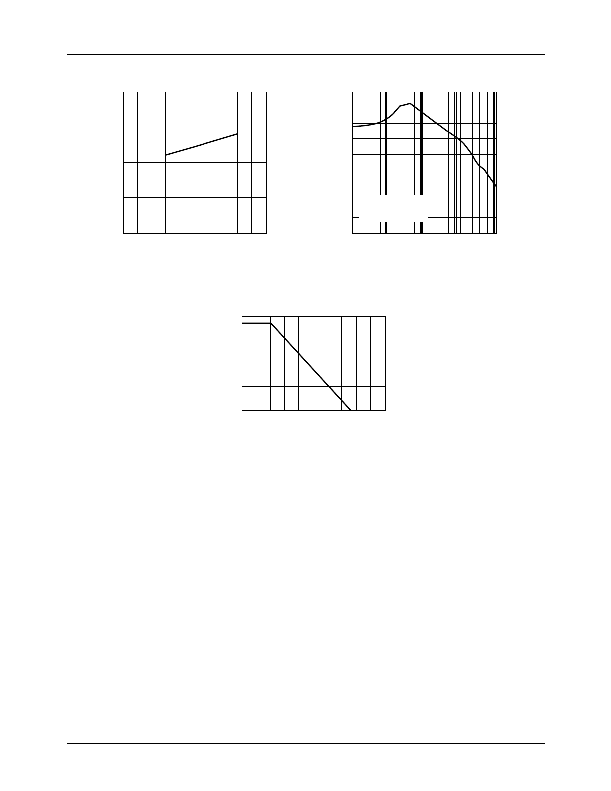
Typical Performance Characteristics (continued)
10
9
8
7
SHORT-CIRCUIT CURRENT (A)
6
-75 -50 -25 0 25 50 75 100 125 150 175
JUNCTION TEMPERATURE (°C)
65-1584-09
90
80
70
60
50
40
30
(VIN – V
20
RIPPLE REJECTIONS (dB)
0.5V ≤ V
I
10
OUT
0
10 100 1K 10K 100K
≤ 3V
OUT)
RIPPLE
= 7A
FREQUENCY (Hz)
≤ 2V
Figure 7. Short-Circuit Current vs. Temperature Figure 8. Ripple Rejection vs. Frequency
20
15
10
POWER (W)
5
65-1584-10
0
50 60 70 80 90 100 110 120 130 140 150
CASE TEMPERATURE (°C)
Figure 9. Maximum Power Dissipation
65-1584-11
REV. 1.0.5 7/13/00 5
Page 6
RC1584 PRODUCT SPECIFICATION
Applications Information
General
D1
The RC1584 and RC1584-1.5 are three-terminal regulators
optimized for GTL+ VTT termination applications. These
devices are short-circuit protected, and offer thermal shutdown to turn off the regulator when the junction temperature
exceeds about 150°C. The RC1584 series provides lo w dropout voltage and fast transient response. Frequency compensation uses capacitors with low ESR while still maintaining
stability. This is critical in addressing the needs of low voltage high speed microprocessor buses like GTL+.
Stability
The RC1584 series require an output capacitor as a part of
the frequency compensation. It is recommended to use a
22µF solid tantalum or a 100µF aluminum electrolytic on the
output to ensure stability. The frequency compensation of
these devices optimizes the frequency response with low
ESR capacitors. In general, it is suggested to use capacitors
with an ESR of <1Ω. It is also recommended to use bypass
capacitors such as a 22µF tantalum or a 100µF aluminum on
the adjust pin of the RC1584 for low ripple and fast transient
response. When these bypassing capacitors are not used at
the adjust pin, larger values of output capacitors provide
equally good results.
Protection Diodes
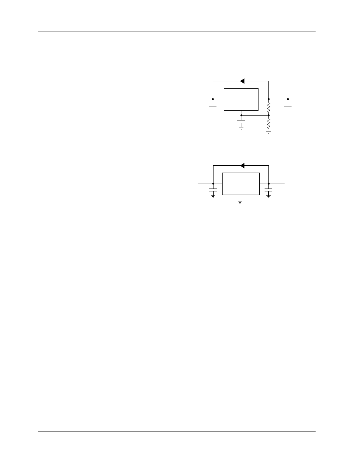
In normal operation, the RC1584 series does not require any
protection diodes. For the RC1584, internal resistors limit
internal current paths on the adjust pin. Therefore, even with
bypass capacitors on the adjust pin, no protection diode is
needed to ensure device safety under shortcircuit conditions.
A protection diode between the input and output pins is usually not needed. An internal diode between the input and output pins on the RC1584 series can handle microsecond surge
currents of 50A to 100A. Even with large value output
capacitors it is difficult to obtain those values of surge currents in normal operation. Only with large values of output
capacitance, such as 1000µF to 5000µF, and with the input
pin instantaneously shorted to ground can damage occur. A
crowbar circuit at the input can generate those levels of current; a diode from output to input is then recommended, as
shown in Figure 10. Usually , normal po wer supply cycling or
system “hot plugging and unplugging” will not generate current large enough to do any damage.
The adjust pin can be driven on a transient basis ±7V with
respect to the output, without any device degradation. As
with any IC regulator, exceeding the maximum input-tooutput voltage differential causes the internal transistors to
break down and none of the protection circuitry is then
functional.
V
V
IN
IN
10µF
10µF
V
V
IN
IN
+
+
C1
C1
+ +
+ +
C1
C1
10µF
10µF
Figure 10. Optional Protection
Ripple Rejection
In applications that require improved ripple rejection, a
bypass capacitor from the adjust pin of the RC1584 to
ground reduces the output ripple by the ratio of V
The impedance of the adjust pin capacitor at the ripple frequency should be less than the value of R1 (typically in the
range of 100Ω to 120Ω) in the feedback divider network in
Figure 10. Therefore, the value of the required adjust pin
capacitor is a function of the input ripple frequency. For
example, if R1 equals 100Ω and the ripple frequency equals
120Hz, the adjust pin capacitor should be 22µF. At 10kHz,
only 0.22µF is needed.
Output V oltage
The RC1584 regulator develops a 1.25V reference voltage
between the output pin and the adjust pin (see Figure 11).
Placing a resistor R1 between these two terminals causes a
constant current to flow through R1 and down through R2 to
set the overall output voltage. Normally, this current is the
specified minimum load current of 10mA.
The current out of the adjust pin adds to the current from R1
and is typically 35µA. Its output voltage contribution is
small and only needs consideration when very precise output
voltage setting is required.
D1
1N4002
1N4002
(OPTIONAL)
(OPTIONAL)
RC1587
RC1584
IN OUT
IN OUT
ADJ
ADJ
+
+
C
C
ADJ
ADJ
D1
D1
1N4002
1N4002
(OPTIONAL)
(OPTIONAL)
RC1587-1.5, -3.3
RC1584-1.5
IN OUT
IN OUT
GND
GND
R1
R1
R2
R2
C2
C2
22µF
22µF
+
+
V
V
OUT
OUT
65-1587-13
65-1584-13
OUT
V
V
C2
C2
22µF
22µF
/1.25V.
OUT
OUT
6 REV. 1.0.5 7/13/00
Page 7
PRODUCT SPECIFICATION RC1584
R
RC1584
C2
22µF
65-1584-14
V
OUT
V
V
IN
OUT
+
= V
REF
IN
C1
10µF
I
ADJ
35µA
(1 + R2/R1) + I
ADJ
OUT
ADJ
(R2)
V
REF
+
R1
R2
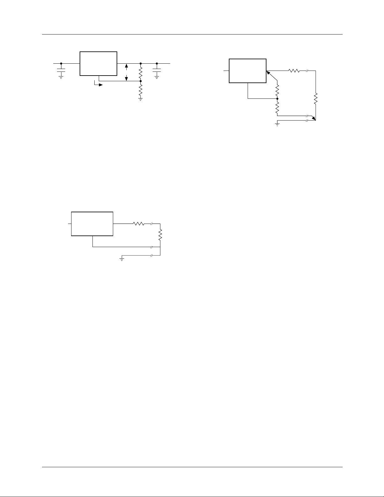
Figure 11. Basic Regulator Circuit
Load Regulation
It is not possible to provide true remote load sensing because
the RC1584 series are three-terminal devices. Load regulation is limited by the resistance of the wire connecting the
regulators to the load. Load regulation per the data sheet
specification is measured at the bottom of the package.
For fixed voltage devices, negative side sensing is a true
Kelvin connection with the ground pin of the device returned
to the negative side of the load. This is illustrated in
Figure 12.
R
P
PARASITIC
LINE RESISTANCE
R
L
V
IN
RC1584-1.5
IN OUT
GND
RC1584
V
IN OUT
IN
ADJ
CONNECT R1 TO CASE
*
CONNECT R2 TO LOAD
LINE RESISTANCE
Figure 13. Connection for Best Load Regulation
Thermal Considerations
The RC1584 series protect themselves under overload conditions with internal power and thermal limiting circuitry.
However, for normal continuous load conditions, do not
exceed maximum junction temperature ratings. It is important to consider all sources of thermal resistance from junction-to-ambient. These sources include the junction-to-case
resistance, the case-to-heat sink interface resistance, and the
heat sink resistance. Thermal resistance specifications have
been developed to more accurately reflect device temperature and ensure safe operating temperatures.
For example, look at using an RC1584T to generate 7A @
P
PARASITIC
R1*
R2*
65-1584-15
R
L
1.5V ± 2% from a 3.3V source (3.135V to 3.465V).
65-1584-17
Figure 12. Connection for Best Load Regulation
For adjustable voltage devices, ne gativ e side sensing is a true
Kelvin connection with the bottom of the output divider
returned to the negative side of the load. The best load regulation is obtained when the top of resistor divider R1 connects directly to the regulator output and not to the load.
Figure 13 illustrates this point.
If R1 connects to the load, then the effective resistance
between the regulator and the load would be:
RP × (1 + R2/R1), R
= Parasitic Line Resistance
P
The connection shown in Figure 13 does not multiply RP by
the divider ratio. As an example, RP is about four milliohms
per foot with 16-gauge wire. This translates to 4mV per foot
at 1A load current. At higher load currents, this drop represents a significant percentage of the overall regulation. It is
important to keep the positive lead between the regulator and
the load as short as possible and to use large wire or PC
board traces.
Assumptions:
•V
= 3.465V worst case
IN
•V
•I
= 1.47V worst case
OUT
= 7A continuous
OUT
•TA = 40°C
• θ
Case-to-Ambient
= 3°C/W (assuming both a heatsink and
a thermally conductive material)
The power dissipation in this application is:
PD = (VIN – V
OUT
) * (I
) = (3.465 – 1.47) * (7) = 13.97W
OUT
From the specification table:
TJ = TA + (PD) * (θ
Case-to-Ambient
+ θJC)
= 40 + (13.97) * (3 + 3) = 124°C
The junction temperature is below the maximum rating.
REV. 1.0.5 7/13/00 7
Page 8
RC1584 PRODUCT SPECIFICATION
Junction-to-case thermal resistance is specified from the IC
junction to the bottom of the case directly below the die. This
is the lowest resistance path for heat flow. Proper mounting
ensures the best thermal flow from this area of the package to
the heat sink. Use of a thermally conductive material at the
U1
V
3.3V
IN
C1
10µF
+
V
IN
C2
100µF
RC1584
ADJ
case-to-heat sink interface is recommended. Use a thermally
conductive spacer if the case of the device must be electrically isolated and include its contribution to the total thermal
resistance. The cases of the RC1584 series are directly connected to the output of the device.
V
V
OUT
+
R1
124Ω
R2
24.9Ω
+
OUT
1.5V
C3
100µF
65-1584-18
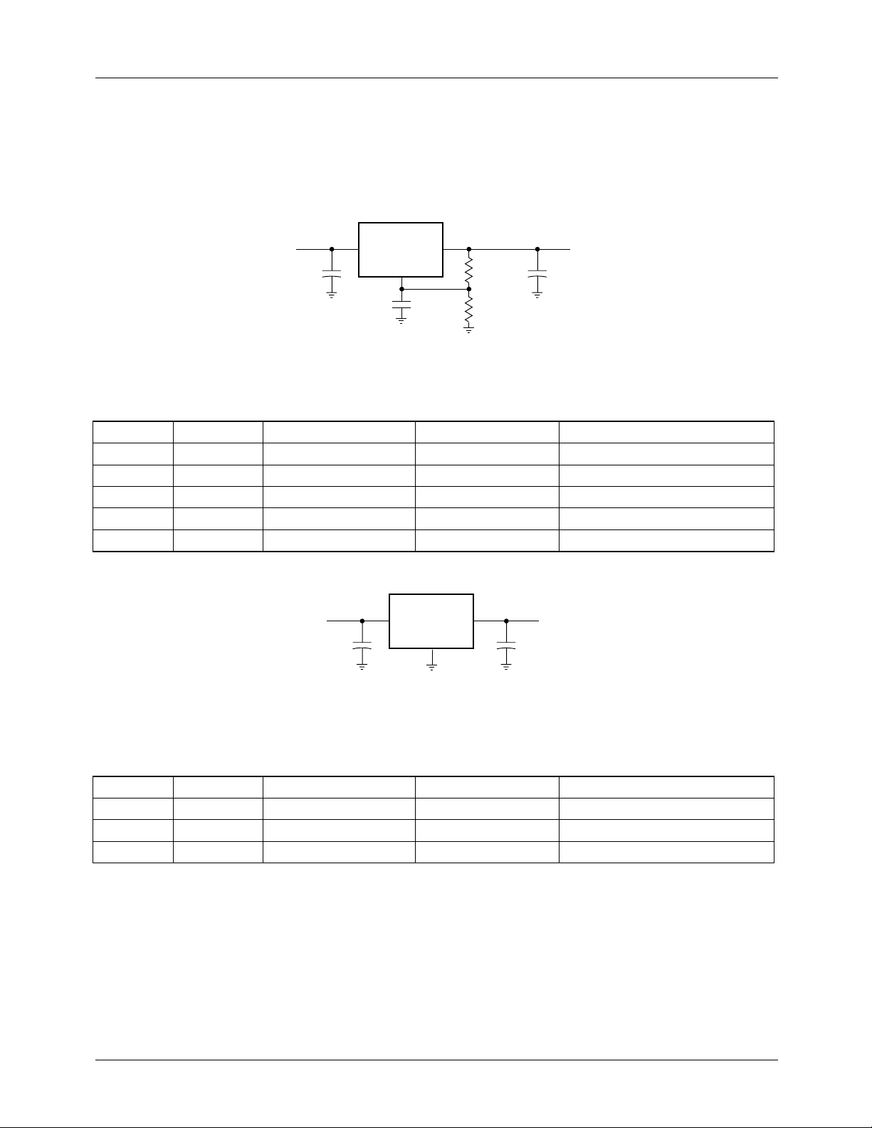
Figure 14. Application Circuit (RC1584)
Table 1. Bill of Materials for Application Circuit for the RC1584
Item Quantity Manufacturer Part Number Description
C1 1 Xicon L10V10 10µF, 10V Aluminum
C2, C3 2 Xicon L10V100 100µF, 10V Aluminum
R1 1 Generic 124Ω, 1%
R2 1 Generic 24.9Ω, 1%
U1 1 Fairchild RC1584T 7A Regulator
U1
+
RC1584-1.5
V
IN
GND
V
OUT
+
V
1.5V
C3
100µF
65-1584-19
OUT
V
3.3V
IN
C1
10µF
Figure 15. Application Circuit (RC1584-1.5)
Table 2. Bill of Materials for Application Circuit for the RC1584-1.5
Item Quantity Manufacturer Part Number Description
C1 1 Xicon L10V10 10µF, 10V Aluminum
C3 1 Xicon L10V100 100µF, 10V Aluminum
U1 1 Fairchild RC1584T-1.5 7A Regulator
8 REV. 1.0.5 7/13/00
Page 9
PRODUCT SPECIFICATION RC1584
Mechanical Dimensions
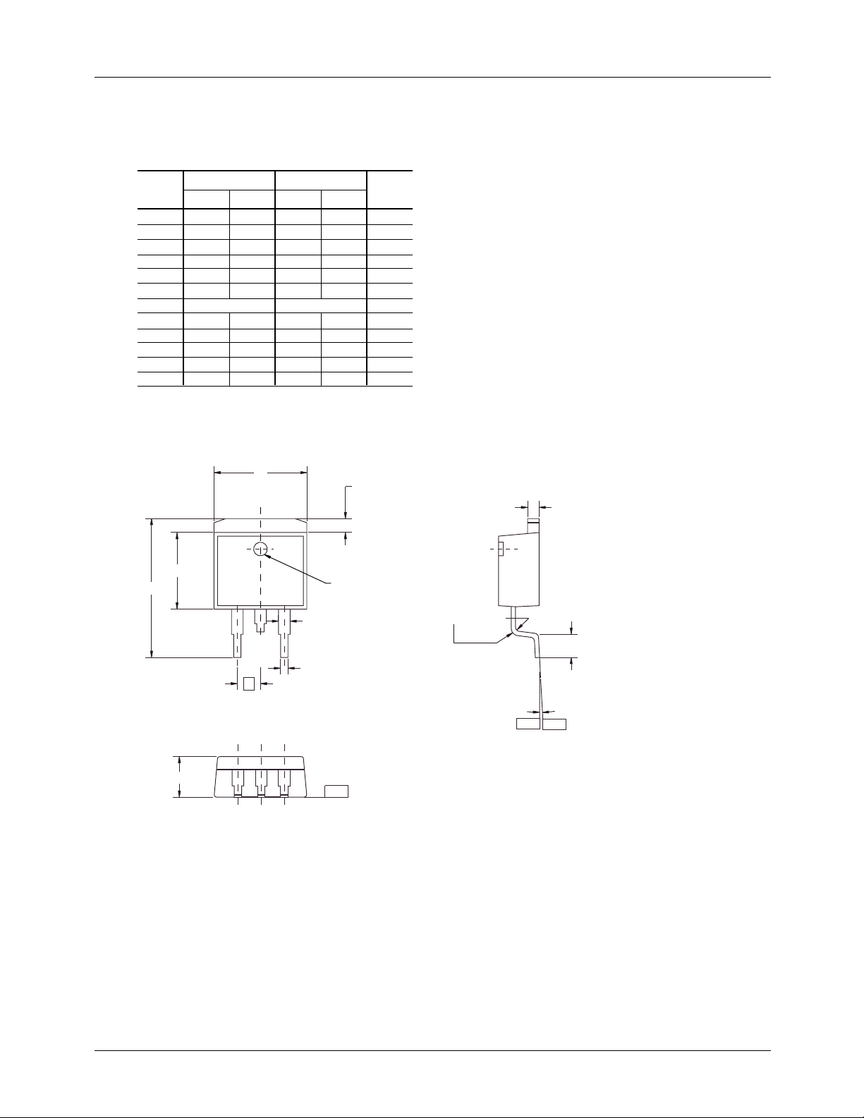
3-Lead TO-263 Package
Symbol
A .160 .190 4.06 4.83
b .020 .036 0.51 0.91
b2
c2
D
E
e
L .575 .625 14.61 15.88
L1
L2
R
α
L
Inches
Min. Max. Min. Max.
.049 .051 1.25 1.30
.045 .055 1.14 1.40
.340 .380 8.64 9.65
.380 .405 9.65 10.29
.100 BSC
.090
.017 .019 0.43 0.78
D
.110
— .055 — 1.40
0° 8° 0° 8°
@PKG/
@HEATSINK
Millimeters
2.54 BSC
2.29 2.79
E
E-PIN
L2
Notes
Notes:
1. Dimensions are exclusive of mold flash and metal burrs.
2. Standoff-height is measured from lead tip with ref. to Datum -B-.
3. Foot length is measured with ref. to Datum -A- with lead surface
(at inner R).
4. Dimensiuon exclusive of dambar protrusion or intrusion.
5. Formed leads to be planar with respect to one another at seating
place -C-.
c2
b2
b
e
A
-C-
R (2 PLCS)
L1
-A--B-
REV. 1.0.5 7/13/00 9
Page 10
RC1584 PRODUCT SPECIFICATION
Mechanical Dimensions (continued)
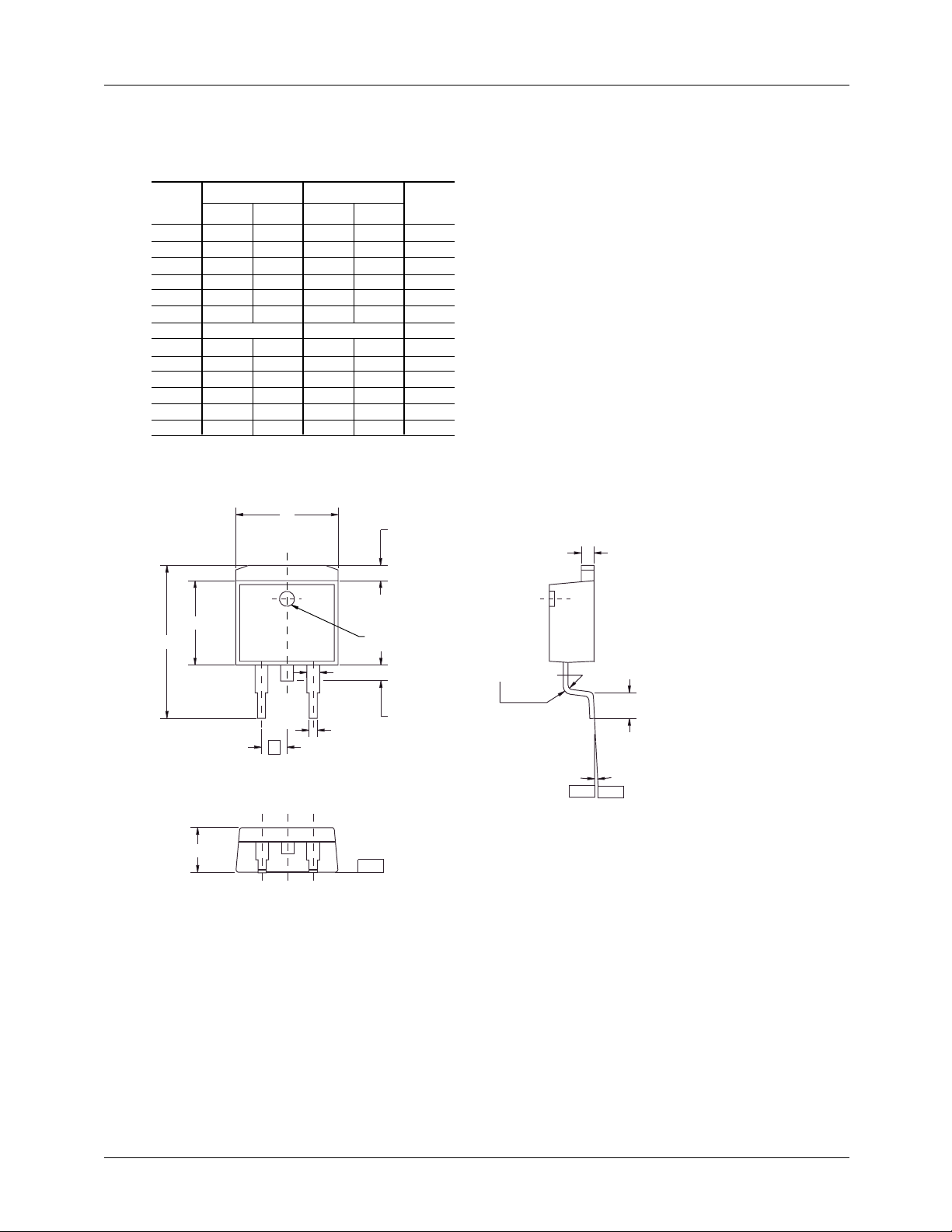
3-Lead TO-263 Center Cut Package
Symbol
A .160 .190 4.06 4.83
b .020 .036 0.51 0.91
b2
c2
D
E
e
L .575 .625 14.61 15.88
L1
L2
L3
R
α
Inches
Min. Max. Min. Max.
.049 .051 1.25 1.30
.045 .055 1.14 1.40
.340 .380 8.64 9.65
.380 .405 9.65 10.29
.100 BSC
.090
.050
.017 .019 0.43 0.78
.110
— .055 — 1.40
.070
0° 8° 0° 8°
@PKG/
@HEATSINK
Millimeters
2.54 BSC
2.29 2.79
1.27 1.78
E
Notes
L2
Notes:
1. Dimensions are exclusive of mold flash and metal burrs.
2. Standoff-height is measured from lead tip with ref. to Datum -B-.
3. Foot length is measured with ref. to Datum -A- with lead surface
(at inner R).
4. Dimensiuon exclusive of dambar protrusion or intrusion.
5. Formed leads to be planar with respect to one another at seating
place -C-.
c2
D
L
E-PIN
b2
b
e
A
L3
-C-
R (2 PLCS)
L1
-A--B-
10 REV. 1.0.5 7/13/00
Page 11
PRODUCT SPECIFICATION RC1584
Mechanical Dimensions (continued)
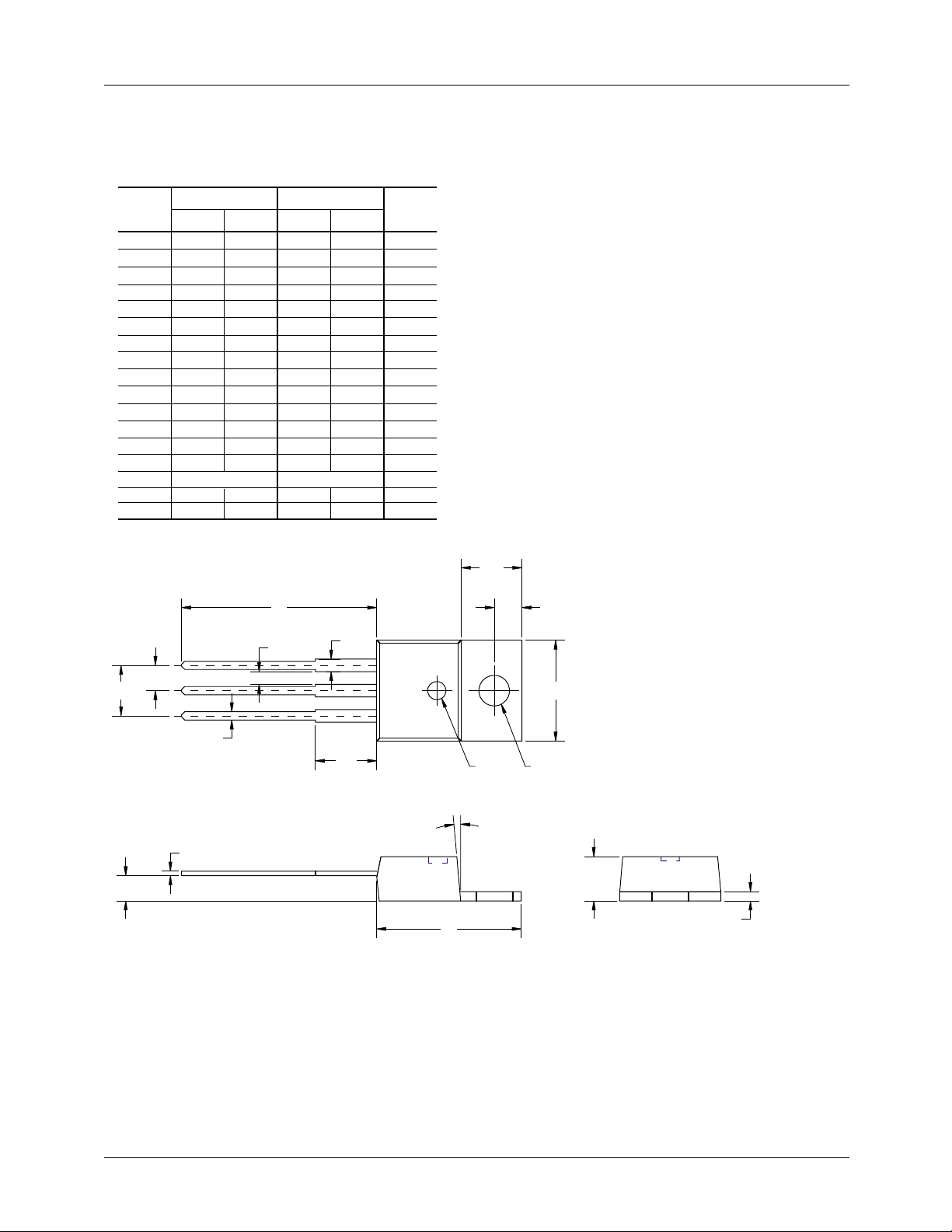
3-Lead TO-220 Package
Symbol
A .140 .190 3.56 4.83
b .015 .040 .38 1.02
b1 .045 1.14
c1 .014 .022 .36 .56
øP .139 .161 3.53 4.09
D .560 .650 14.22 16.51
E
e
e1 .190 .210 4.83 5.33
e3
F
H1 .230 .270 5.94 6.87
J1
L
L1
Q
α
Inches
Min. Max. Min. Max.
.070 1.78
.380 .420 9.65 10.67
.090 .110 2.29 2.79
.045 — 1.14 —
.020 .055 .51 1.40
.080 .115 2.04 2.92
.500 .580 12.70 14.73
.100 .135 2.54 3.43
3° 7° 3° 7°
Millimeters
6.35 BSC.250 BSC
L
e3
b1
Notes
Notes:
1. Dimension c1 apply for lead finish.
H1
Q
e1
J1
e
E
b
L1
E-PIN øP
(5X)
α
c1
A
D
F
REV. 1.0.5 7/13/00 11
Page 12
RC1584 PRODUCT SPECIFICATION
Ordering Information
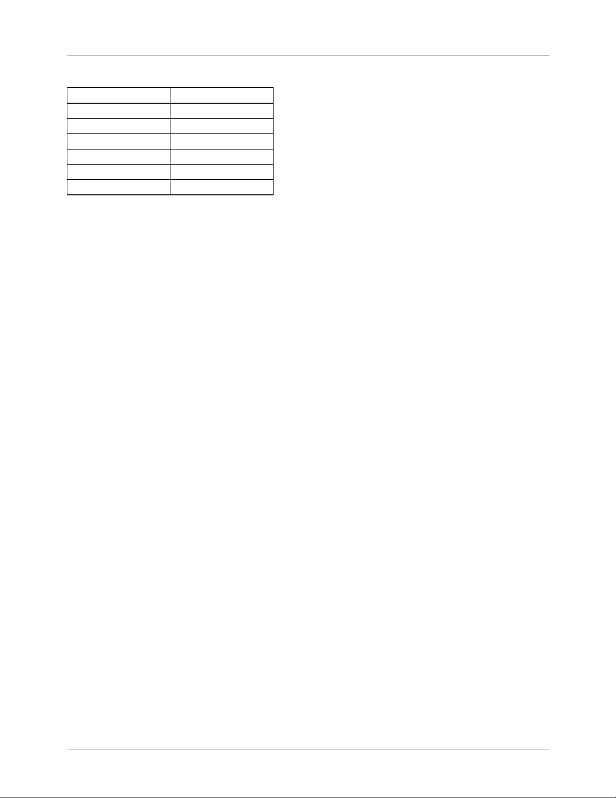
Product Number Package
RC1584M TO-263
RC1584MC TO-263 center cut
RC1584T TO-220
RC1584M-1.5 TO-263
RC1584MC-1.5 TO-263 center cut
RC1584T-1.5 TO-220
LIFE SUPPORT POLICY
FAIRCHILD’S PRODUCTS ARE NOT AUTHORIZED FOR USE AS CRITICAL COMPONENTS IN LIFE SUPPORT DEVICES
OR SYSTEMS WITHOUT THE EXPRESS WRITTEN APPROVAL OF THE PRESIDENT OF FAIRCHILD SEMICONDUCTOR
CORPORATION. As used herein:
1. Life support devices or systems are devices or systems
which, (a) are intended for surgical implant into the body,
or (b) support or sustain life, and (c) whose failure to
perform when properly used in accordance with
instructions for use provided in the labeling, can be
reasonably expected to result in a significant injury of the
user.
2. A critical component in any component of a life support
device or system whose failure to perform can be
reasonably expected to cause the failure of the life support
device or system, or to affect its safety or effectiveness.
www.fairchildsemi.com
7/13/00 0.0m 001
1998 Fairchild Semiconductor Corporation
Stock#DS30001584
 Loading...