

Page 1
www.fairchildsemi.com
RC0431A (RC431A)
Low-Voltage Adjustable Precision Shunt Regulator
Features
•Low voltage operation to 1.24V
• 1% reference voltage tolerance
• Output voltage adjustable from V
•Low 80µA operational cathode current
• 0.25Ω typical output impedance
•TO-92, SOT23-3 and SOT23-5 packages
to 12V
ref
Applications
•Voltage reference for discrete power circuits
Description
The RC0431A is a low-voltage 3-terminal adjustable
precision voltage reference regulator. It has an excellent
thermal stability over the standard commercial temperature
range. The output voltage can be set to any value between
Vref (1.24V) and 12V using two external resistors. The
RC0431A operates from a lower voltage (1.24V) than the
traditional shunt regulator references which operate from
2.5V. When used with an optocoupler, the RC0431A will be
an ideal voltage reference in an isolated feedback circuit for
use in switched-mode power supplies and modular DC-DC
converters. The RC0431A has a low output impedance of
active output circuitry offering a very sharp turn-on
characteristic. The RC0431A will be an excellent
replacement for low-voltage zener diodes in many
applications such as on-board regulation and adjustable
power supplies.
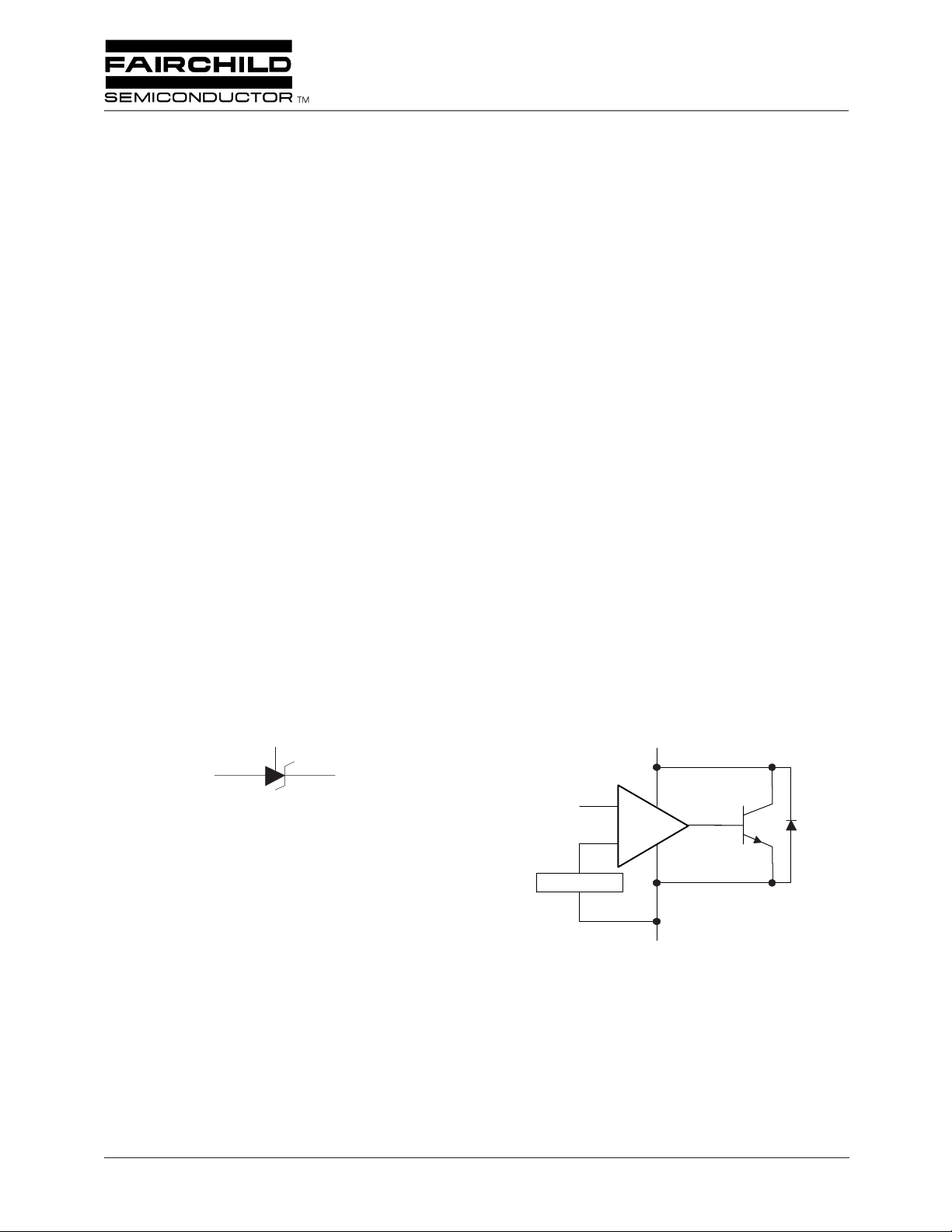
Symbol Block Diagram
REF
Anode Cathode
65-431A-01
REF
V
= 1.24V
ref
CATHODE
+
_
65-431A-02
ANODE
REV. 1.0.7 8/5/03
Page 2
RC0431A (RC431A) PRODUCT SPECIFICATION
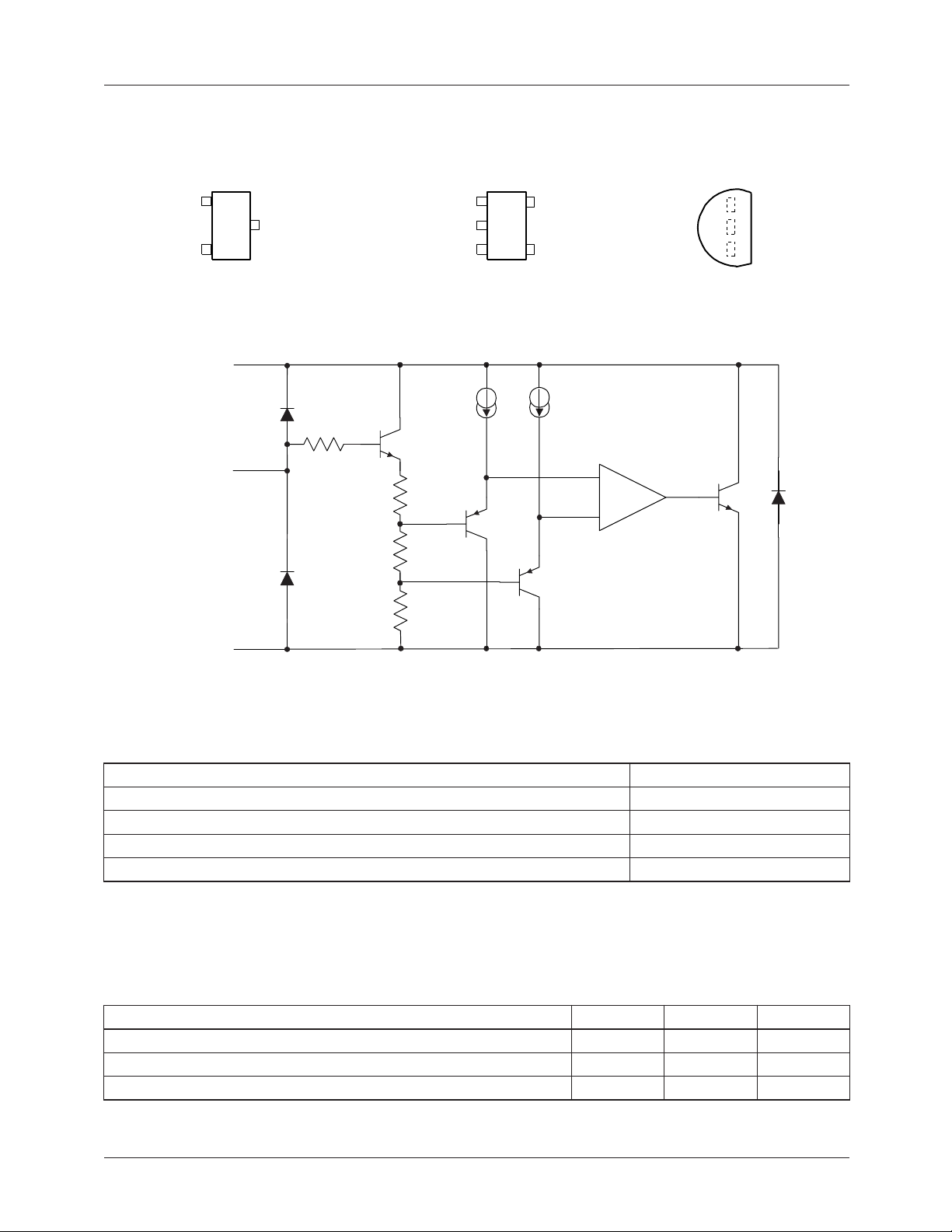
Pin Assignments
SOT-23 PACKAGE (3-Lead)
(TOP VIEW)
REF
1
3
CATHODE
2
Equivalent Schematic
CATHODE
REF
ANODE
SOT-23 PACKAGE (5-Lead)
(TOP VIEW)
1
5
NC
2
NC
CATHODE
NC = No internal connection
34
ANODE
REF
TO-92 PACKAGE
(TOP VIEW)
CATHODE
ANODE
REF
65-431A-03
A
ANODE
65-431A-04
Absolute Maximum Ratings
Ratings are over full operating free-air temperature range unless otherwise noted.
Cathode voltage, V
KA
Continuous cathode current I
Reference current, I
ref
K
13.2V
–20mA to 20mA
–0.05mA to 3mA
Power dissipation See Dissipation Rating Table
Storage temperature range -65° to 150°C
Notes:
1. Functional operation under these conditions is not implied. Permanent damage may occur if the device is subjected to
conditions outside these ratings.
Recommended Operating Conditions
Parameter Min. Max. Units
Cathode voltage, V
Cathode current, I
Operating temperature range in free-air, T
V
KA
K
A
REF
0.1 15 mA
070°C
12 V
2 REV. 1.0.7 8/5/03
Page 3
PRODUCT SPECIFICATION RC0431A (RC431A)
Dissipation Rating Table
Package
Power Rating
TA ≤ 25°C
Derating Factor
TA ≥ 25°C
Power Rating
TA = 70°C
TO-92 775mW 6.2mW/OC 496mW
o
SOT23-5 150mW 1.2mW/
C 96mW
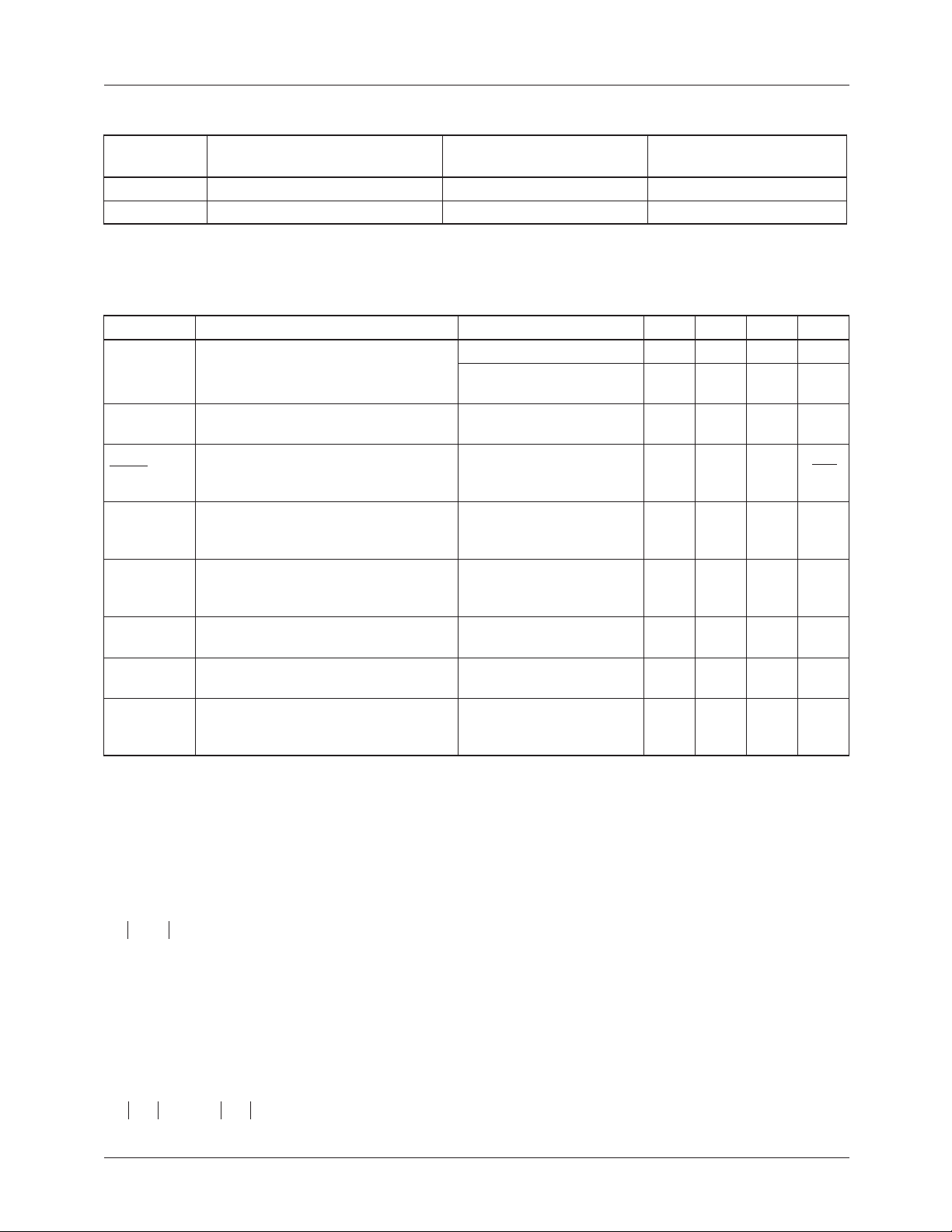
Electrical Specifications
TA = 25°C (unless otherwise noted), at free-air
Symbol Parameters Conditions Min. Typ. Max. Units
V
ref
V
ref (dev)
∆V
ref
∆V
KA
I
ref
I
ref(dev)
I
K(min)
I
off
|ZKA| Dynamic impedance (see note 3) VKA = V
Reference Voltage VKA = V
ref
IK = 10mA,
TA = 0 to 70°C
V
deviation over full temperature
ref
range (see note 2)
Ratio of V
change in cathode
ref
voltage change
VKA = V
ref
See note 2 and Figure 1.
IK = 10mA,
∆VKA = V
ref
See figure 2.
Reference terminal current IK = 10mA,
R1 = 10KΩ, R2 = ∞
See figure 2.
I
deviation over full temperature
ref
range (see note 2)
IK = 10mA,
R1 = 10KΩ, R2 = ∞
See note 1 & figure 2.
Minimum cathode current for
regulation
VKA = V
ref
See figure 1.
Off-state cathode current VKA = 6V, V
See figure 3.
IK = 0.1mA to 15mA,
ref
See figure 1.
, TA = 25°C 1.228 1.24 1.252 V
1.221 1.259
, IK = 10mA,
412mV
-1.5 -2.7 mV
to 6V.
0.15 0.5 µA
0.05 0.3 µA
= 0
ref
, f ≤ 1KHz
55 80 µA
0.001 0.1 µA
0.25 0.4 Ω
V
Notes:
1. Functional operation under these conditions is not implied. Permanent damage may occur if the device is subjected to
conditions outside these ratings.
2. Full temperature range is 0°C to 70°C.
3. The deviation parameters V
obtained over the rated temperature range. The average full-range temperature coefficient of the reference input voltage,
∞V
, is defined as:
ref
V
ref dev()VrefTA
----------------------------------------------------------------------------------------------
∞V
where ∆T
∞V
temperature.
4. The dynamic impedance is defined as: Z
When the device is operating with two external resistors (see Figure 2), the total dynamic impedance of the circuit is given
by:
Z
REV. 1.0.7 8/5/03 3
ppm/°C〈〉
ref
is the rated operating free-air temperature range of the device.
A
can be positive or negative depending on whether minimum V
ref
∆V
--------
KA
∆I
=
×≈=
Z
KA
1
ref(dev)
R
1
-------+
R
2
and I
are defined as the differences between the maximum and minimum values
ref(dev)
25°C=〈〉⁄{}106×
∆T
A
= ∆VKA/ ∆I
KA
or maximum V
ref
K
, respectively, occurs at the lower
ref
Page 4
RC0431A (RC431A) PRODUCT SPECIFICATION
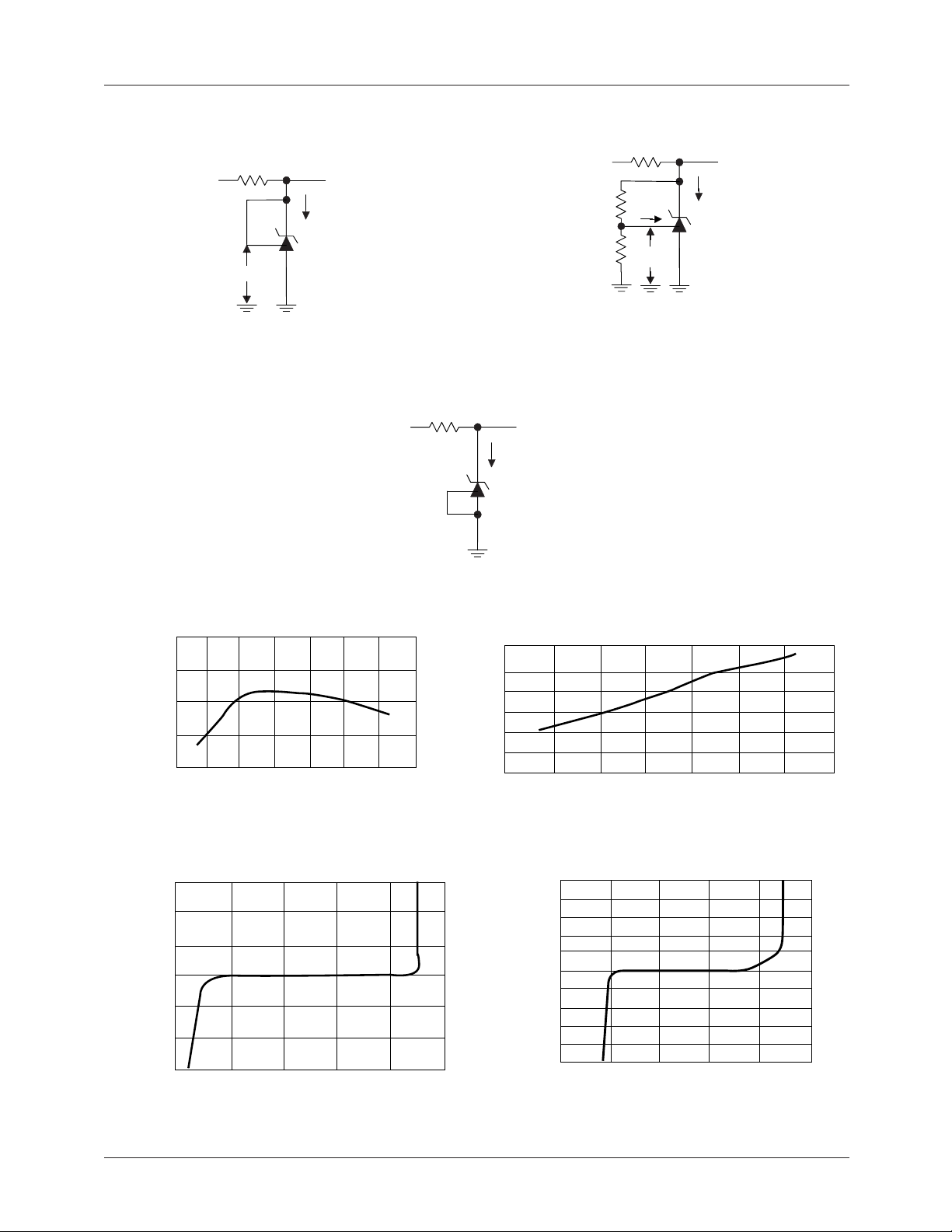
Parameter Measurement Information
I
K
V
OUT
65-431A-06
V
V
IN
V
ref
I
K
V
OUT
65-431A-05
IN
R1
I
ref
R2
V
ref
Figure 1. Test Circuit for Figure 2. Test Circuit for
V
= V
KA
REF
, V
= VKA = V
OUT
REF
V
IN
VKA > V
I
Figure 3. Test Circuit for I
V
OFF
65-431A-07
REF
OUT
OFF
, V
= VKA = V
OUT
x (1+R1/R2) + I
REF
REF
x R1
lk = 10 mA
1.250
1.246
1.242
1.238
1.230
Vref–Reference Voltage (V)
–20–40 200406080100
Tj—Junction Temp. (°C)
lk = 10 mA, R1 = 10 kΩ, R2 = infinite
250
200
150
100
50
–40 –20 0 20 40 60 80 100
Iref–Reference Input Current (nA)
Tj—Junction Temp. (°C)
Figure 4. Reference Voltage vs. Junction Temp. Figure 5. Reference Input Current vs. Junction Temp.
15
V
KA
= Vref, T = 25°C
150
KA
= Vref, T = 25°C
V
120
10
5
0
90
60
30
0
–30
–5
lk–Cathode Current (mA)
–10
–15
–0.5-1 0 0.5 1 1.5
VKA–Cathode Voltage (V)
lk–Cathode Current (µA)
–120
–150
–60
–90
–0.5–1 0 0.5 1 1.5
VKA–Cathode Voltage (V)
Figure 6. Cathode Current vs. Cathode Voltage Figure 7. Cathode Current vs. Cathode Voltage
4 REV. 1.0.7 8/5/03
Page 5
PRODUCT SPECIFICATION RC0431A (RC431A)
= 6V, Vref = 0V
V
KA
40.0
30.0
20.0
10.0
0.0
–40 0–20 20 40 60 80 100
Ioff–Off State Cathode Current (nA)
Tj—Junction Temperature (°C)
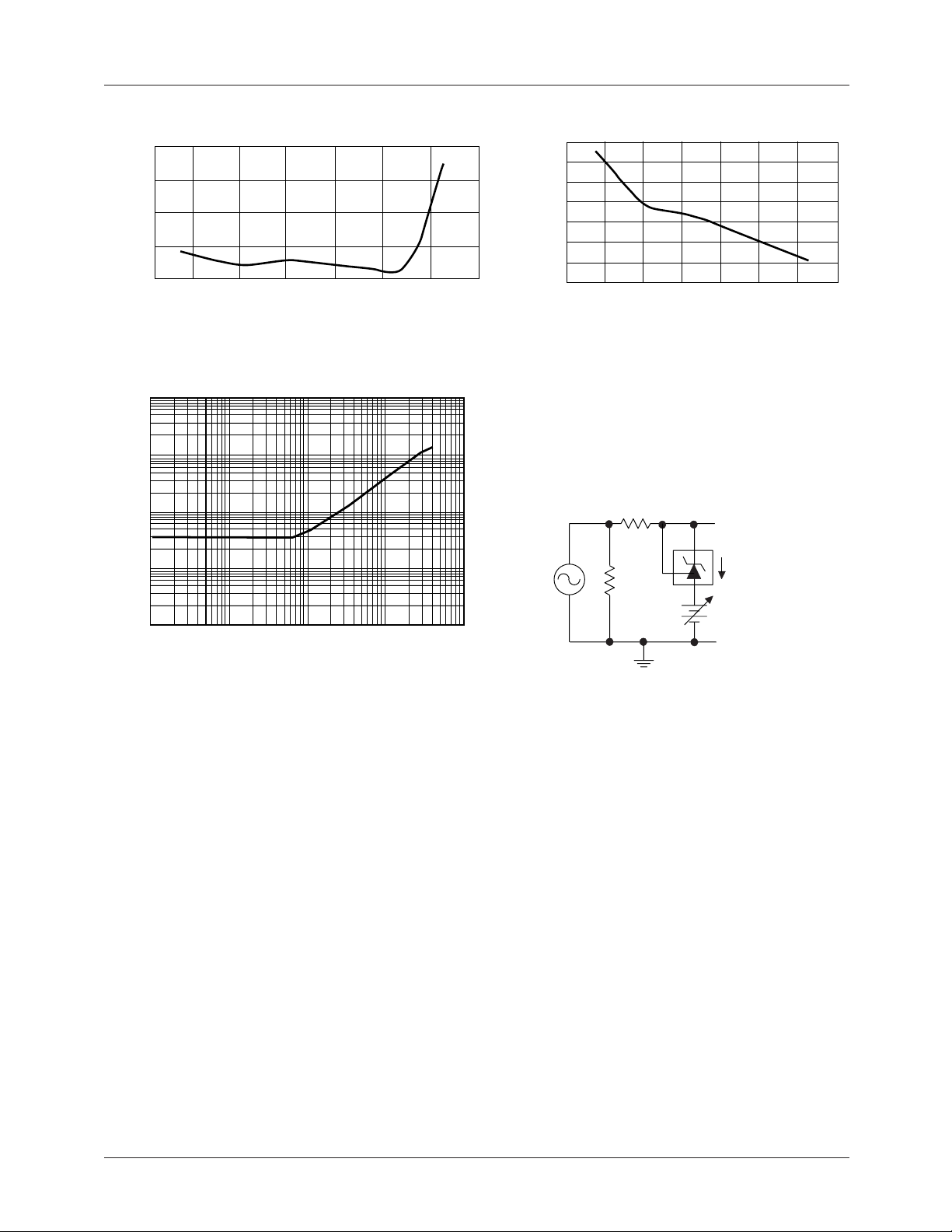
Figure 8. Off-State Cathode Current vs. Figure 9. Ratio of Delta Reference Voltage
Junction Temperature to Delta Cathode Voltage vs. Junction Temperature
100
10
1
0.1
|Zka|–Reference Impedance (Ω)
lk = 10 mA, Del V
1.4
1.2
1.0
0.8
0.6
0.4
0.2
Del Vref / Del Vka (mV/V)
0.0
–40 –20 0 20 40 60 80 100
100Ω
100Ω
= Vref to 6V
KA
Tj—Junction Temperature (°C)
OUTPUT
I
K
+
0.01
10000 100000
f–Frequency (Hz)
1000000 100000001000
GND
Figure 10. Reference Impedance vs. Frequency Figure 11. Test Circuit for Reference Impedance
REV. 1.0.7 8/5/03 5
Page 6
RC0431A (RC431A) PRODUCT SPECIFICATION
Mechanical Dimensions
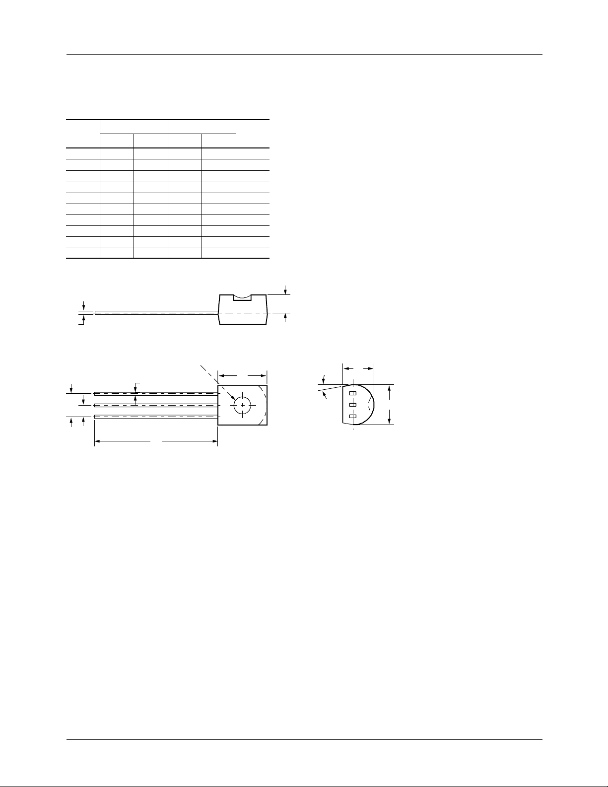
TO-92 Package
Symbol
A .170 .210
b .015 .021
c .014
øD .175 .205
E .125 .165
e .095 .105 2.41 2.67
e1 .045 .055
L
S
α
c
e
e1
Inches
Min. Max. Min. Max.
.020
.500 —
.080 .115
4° 6°
b
Millimeters
4.32 5.33
.38 .53
.36
4.45 5.21
3.18 4.19
1.14 1.40
12.70 —
2.03 2.92
4° 6°
E-PIN C 1/16
.51
Notes
A
Notes:
1. 2.Package outline exclusive of any mold flashes dimension.
Package outline exclusive of burr dimension.
S
α
E
øD
L
6 REV. 1.0.7 8/5/03
Page 7
PRODUCT SPECIFICATION RC0431A (RC431A)
Mechanical Dimensions (continued)
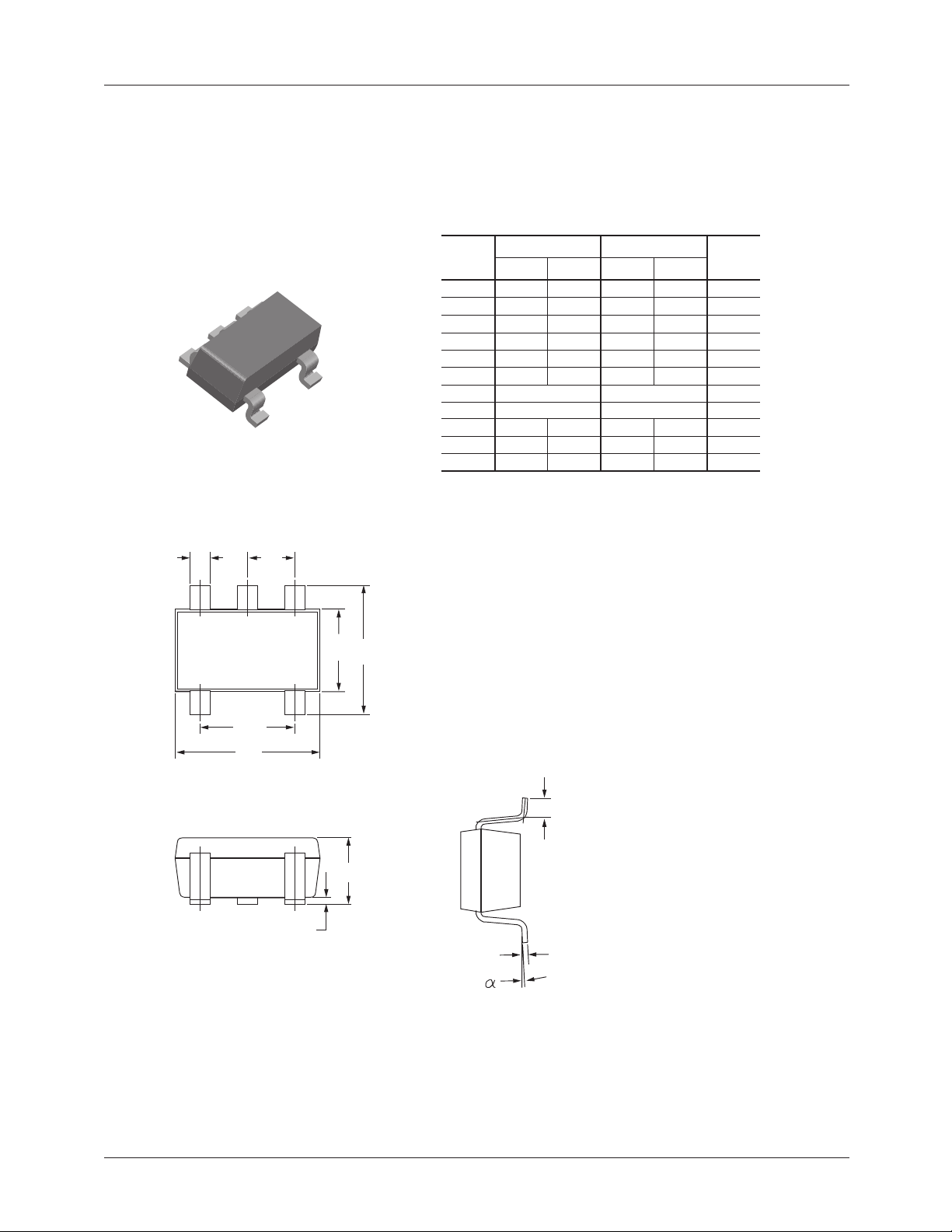
SOT23-5 Package
SOT23 5-Lead
Symbol
A .035 .057
A1 .000 .006
B
c .003
D .106 .122
E .059
e
e1
H .087 .126
L
Notes:
1.
Package outline exclusive of mold flash & metal burr.
2.
Package outline exclusive of solder plating.
3.
B
e
EIAJ Ref Number SC-74A.
Inches
Min. Max. Min. Max.
.008
.004 .024 .10 .60
0 10
.020
.010
.071
.037 BSC
.075 BSC
Millimeters
.90 1.45
.00 .15
.20
.08 .25
2.70
1.50 1.80
2.20 3.20
0 10
.50
3.10
.95 BSC
1.90 BSC
Notes
E
H
e1
D
L
A
A1
c
REV. 1.0.7 8/5/03 7
Page 8
RC0431A (RC431A) PRODUCT SPECIFICATION
Mechanical Dimensions (continued)
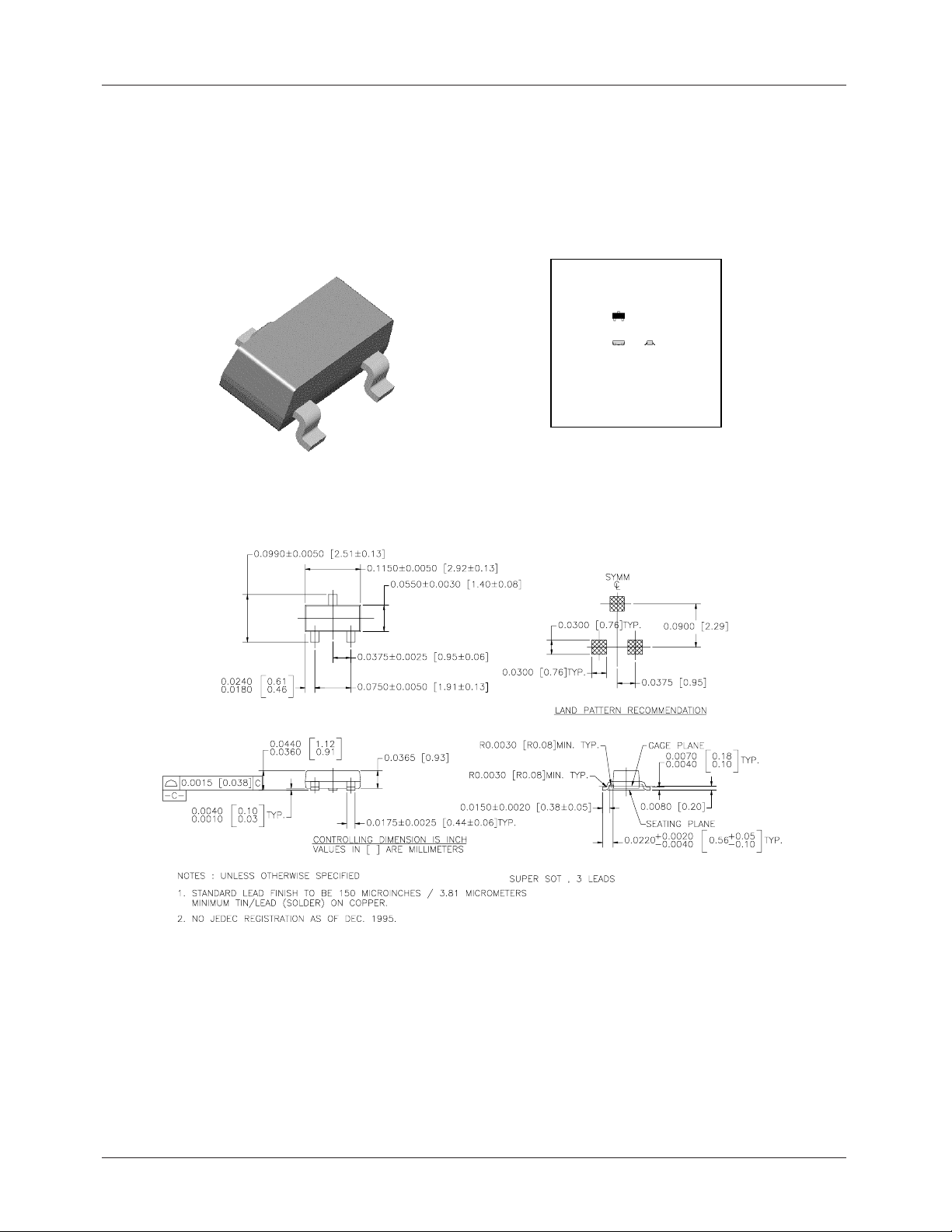
SuperSOT™-3 Package
SuperSOT-3 (FS PKG Code 32)
1 : 1
Scale 1:1 on letter size paper
Di mensi ons sh own below are in:
inches [millimeters]
Part Weight per unit (gram): 0.0097
8 REV. 1.0.7 8/5/03
Page 9

RC0431A (RC431A) PRODUCT SPECIFICATION
Ordering Information
Product Number Package
RC0431AM SOT23-5
RC0431AT TO-92
RC0431AS SOT23-3
DISCLAIMER
FAIRCHILD SEMICONDUCTOR RESERVES THE RIGHT TO MAKE CHANGES WITHOUT FURTHER NOTICE TO
ANY PRODUCTS HEREIN TO IMPROVE RELIABILITY, FUNCTION OR DESIGN. FAIRCHILD DOES NOT ASSUME
ANY LIABILITY ARISING OUT OF THE APPLICATION OR USE OF ANY PRODUCT OR CIRCUIT DESCRIBED HEREIN;
NEITHER DOES IT CONVEY ANY LICENSE UNDER ITS PATENT RIGHTS, NOR THE RIGHTS OF OTHERS.
LIFE SUPPORT POLICY
FAIRCHILD’S PRODUCTS ARE NOT AUTHORIZED FOR USE AS CRITICAL COMPONENTS IN LIFE SUPPORT DEVICES
OR SYSTEMS WITHOUT THE EXPRESS WRITTEN APPROVAL OF THE PRESIDENT OF FAIRCHILD SEMICONDUCTOR
CORPORATION. As used herein:
1. Life support devices or systems are devices or systems
which, (a) are intended for surgical implant into the body,
or (b) support or sustain life, and (c) whose failure to
perform when properly used in accordance with
instructions for use provided in the labeling, can be
reasonably expected to result in a significant injury of the
user.
2. A critical component in any component of a life support
device or system whose failure to perform can be
reasonably expected to cause the failure of the life support
device or system, or to affect its safety or effectiveness.
www.fairchildsemi.com
8/5/03 0.0m 002
2003 Fairchild Semiconductor Corporation
Stock#DS3000431A
 Loading...