

Page 1
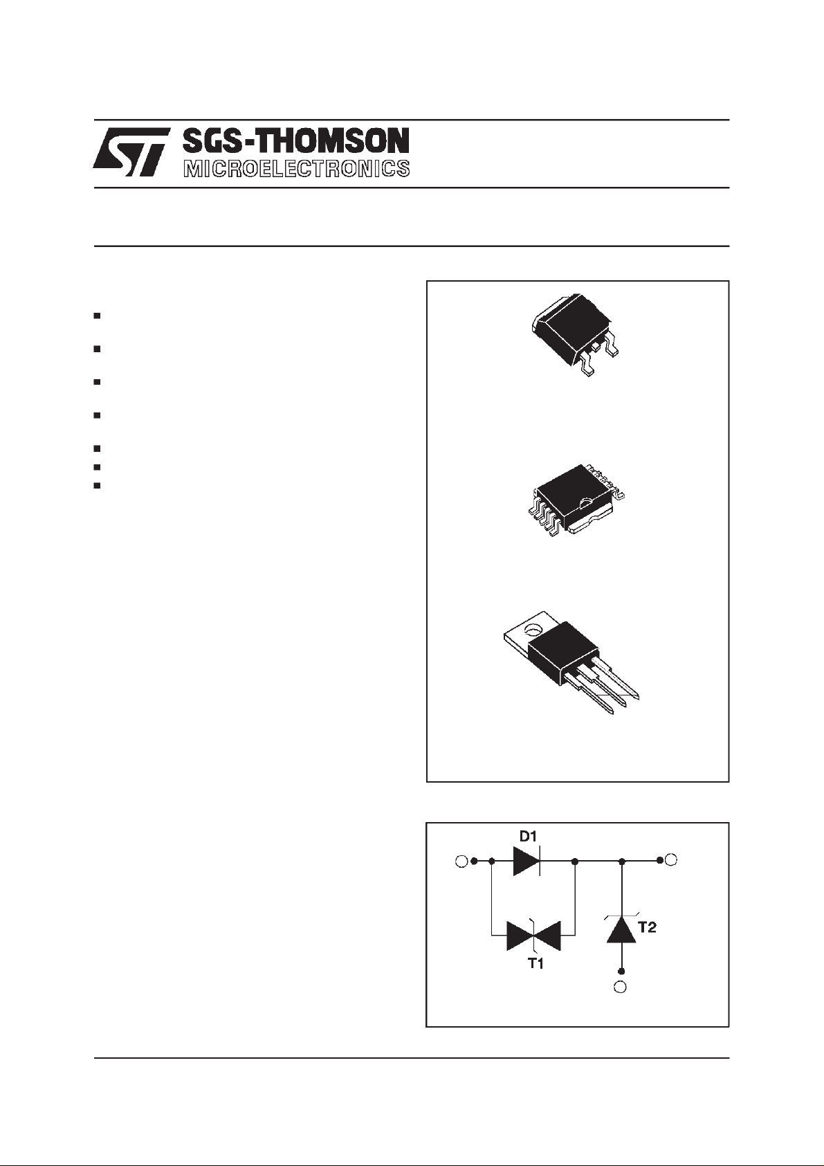
RBO08-40G/M/T
ApplicationSpecificDiscretes
A.S.D.
FEATURES
8ADIODETOGUARDAGAINSTBATTERYREVERSAL.
NEGATIVEOVERVOLTAGEPROTECTIONBY
CLAMPING.
COMPLIANTWITHISO/DTR7637STANDARD
FORPULSES 1, 2,3a and 3b.
SUITABLE FOR AUTOPROTECTED ALTERNATORENVIRONMENT.
BREAKDOWNVOLTAGE: 24V min.
CLAMPINGVOLTAGE:± 40 V max.
MONOLITHIC STRUCTURE FOR GREATER
RELIABILITY.
DESCRIPTION
Designedto protectagainstbatteryreversaland
overvoltagesin automotiveapplications,this
monolithiccomponentoffersmultiplefunctionsin
the samepackage:
D1 : reversedbattery protection
T1 : clampingagainst negativeovervoltages
T2 : Transilfunctionfor overvoltageprotection.
TM
OVERVOL TAGEPROTECT IONCIRCUI T (RBO)
REVERSEDBATTERYAND
D2PAK
RBO08-40G
PowerSO-10
RBO08-40M
TM
January1998 - Ed : 2
TO220AB
RBO08-40T
FUNCTIONAL DIAGRAM
1
3
2
1/14
Page 2
RBO08-40G / RBO08-40M / RBO08-40T
ABSOLUTE MAXIMUM RATINGS
Symbol Parameter Value Unit
I
FSM
Non repetitivesurgepeak forward current
tp = 10 ms 80 A
(DiodeD1)
I
F
P
PP
DC forwardcurrent(Diode D1) Tc = 75°C8 A
PeakpulsepowerbetweenInput andOutput
10/1000µs 600 W
(TransilT1) seenote 1 Tjinitial= 25°C
P
PP
T
stg
Tj
T
L
PeakpulsepowerbetweenPins 3 and 2 (10/1000µs) 1500 W
Storagetemperature range
Maximumjunction temperature
Maximumlead temperaturefor solderingduring 10 s
- 40 to+ 150
150
260 °C
at 4.5mm from case for TO220AB
Note 1 : for a surge greater than themaximum value, thedevice will fail inshort-circuit..
TM :PowerSO-10,TRANSIL and ASD are trademarks ofSGS-THOMSON Microelectronics.
THERMAL RESISTANCE
Symbol Parameter Value Unit
Rth (j-c)
Junctionto case
RBO08-40M
RBO08-40G
RBO08-40T
2.4
2.4
2.4
°C
°C/W
2/14
D1
T1
V
V
31 VRM31
CL
I13
31
F
I
T2
2
31
BR
V
IRM31
31
I
R
Ipp31
F13
V13
Ipp32
I
RM
I32
IR32
32
VRM32 V
32 V
R
B
1
V32
32
C
L
3
2
Page 3
RBO08-40G / RBO08-40M / RBO08-40T
Symbol Parameter
V
RM31/VRM32
V
BR31/VBR32
I
R31/IR32
V
CL31/VCL32
V
F13
I
PP
αT
C
31/C32
Stand-offvoltage Transil T1 / TransilT2.
Breakdownvoltage TransilT1 / TransilT2.
LeakagecurrentTransil T1 / TransilT2.
ClampingvoltageTransil T1 / TransilT2.
Forwardvoltagedrop DiodeD1.
Peak pulsecurrent.
Temperaturecoefficientof V
BR
.
CapacitanceTransil T1 / TransilT2.
ELECTRICAL CHARACTERISTICS: DIODED1 (- 40°C< T
amb
Symbol Test Conditions
V
F13
IF=8A
RBO08-40M/G
RBO08-40T
V
F13
=8A@T
I
F
IF=4A
=25°C 1.45 V
amb
RBO08-40M/G
RBO08-40T
I
V
F13
=4A@T
F
IF= 1A 1.1 V
I
=1A@T
F
= 1A@ Tj= 85°C 0.9 V
I
F
=25°C
amb
=25°C 1.0 V
amb
ELECTRICAL CHARACTERISTICS: TRANSIL T1 (- 40°C<T
Symbol Test Conditions
V
BR 31
V
BR 31
I
RM31
I
RM31
V
CL31
αT TemperaturecoefficientofV
C
31
IR=1 mA 22 35 V
IR=1 mA, T
=25°C2432V
amb
VRM=20V 50 µA
VRM=20V,T
IPP=15A,Tjinitial=25°C
amb
=25°C
10/1000µs40V
BR
F = 1MHz VR= 0 V 1000 pF
<+85°C)
<+85°C)
amb
Value
Min. Typ. Max.
1.5 V
1.7 V
1.3 V
1.35 V
1.2 V
Value
Min. Typ. Max.
10 µA
910-4/°C
Unit
Unit
ELECTRICAL CHARACTERISTICS: TRANSIL T2 (- 40°C<T
Symbol Test Conditions
V
BR 32
V
BR 32
I
RM 32
I
RM 32
V
CL 32
αT
C
32
IR=1 mA 22 35 V
IR=1 mA, T
=25°C2432V
amb
VRM=20V 50 µA
VRM=20V,T
IPP= 37.5 A
Temperaturecoefficientof V
=25°C10µA
amb
10/1000µs40V
BR
F = 1MHz VR=0 V 2000 pF
amb
<+85°C)
Value
Min. Typ. Max.
Unit
8.5 10-4/°C
3/14
Page 4
RBO08-40G / RBO08-40M / RBO08-40T
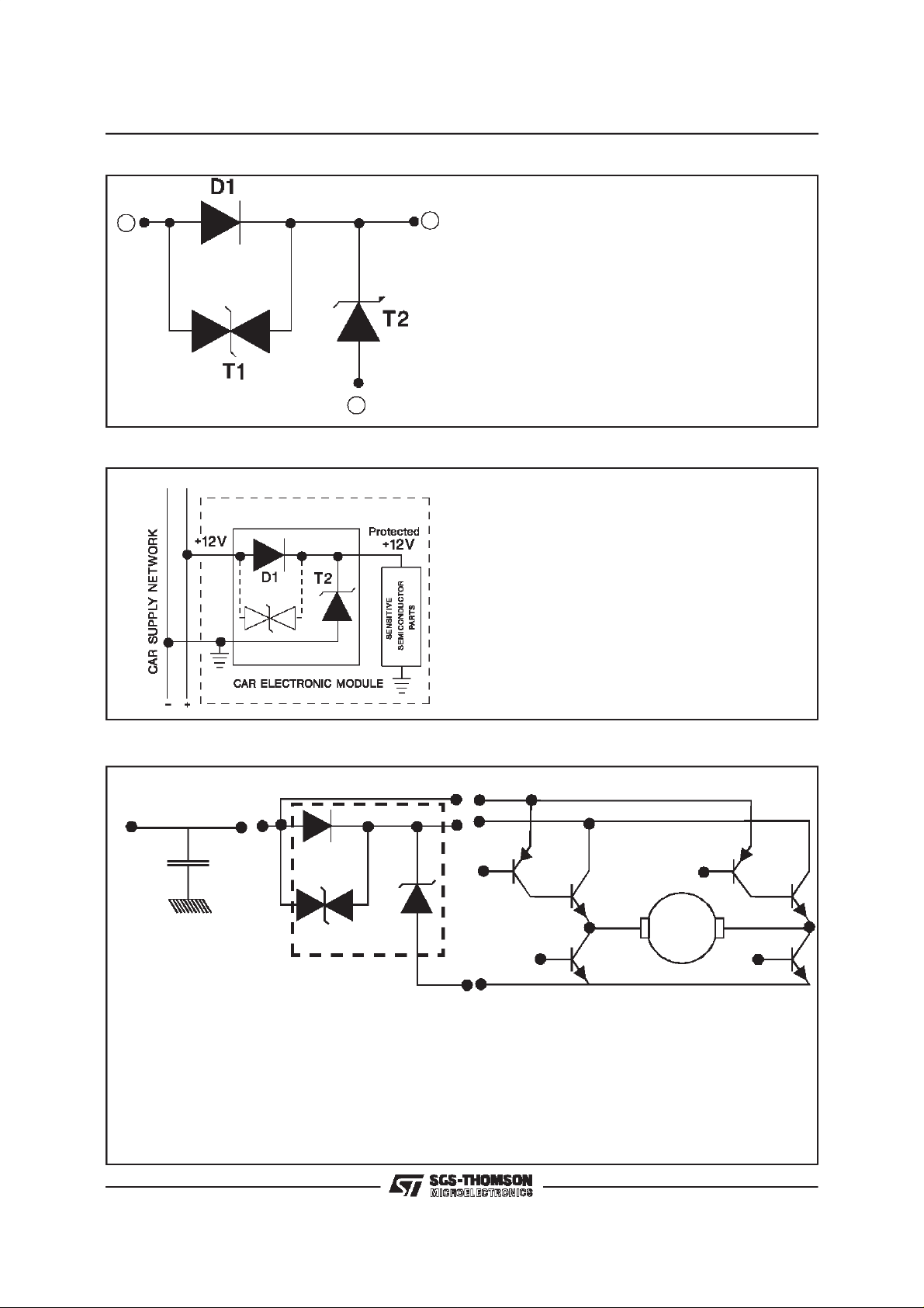
PRODUCTDESCRIPTION
1
2
BASICAPPLICATION
TheRBO has 3 functionsintegratedon thesame
3
chip.
D1 : “Diode function”in order to protect against
reversedbattery operation.
T2:“Transil function” in order to protect against
positive surge generated by electric systems
(ignition, relay. ...).
T1 : Protection againt negative surges such as
inductive overvoltages (see motor application
below).
* The monolithic multi-function protection
(RBO) has been developed to protect
sensitivesemiconductorsin car e lect ronic
modules against both overvoltage and
batteryreverse.
* In addition, the RBO circuit prevents
overvoltages generated by the module from
affecting the carsupply network.
MOTORDRIVER APPLICATION
BATTERY
Filter
D1
T2
T1
MOTOR
RBO
DEVICE MOTOR CONTROL
In thisapplication,onehalfofthemotordrivecircuitis suppliedthroughthe “RBO”and isthusprotected
as per its basic function application.
The secondpart is connecteddirectlyto the “carsupplynetwork” andis protectedas follows:
- Forpositive surges: T2 (clampingphase) and D1 in forward-biased.
- Fornegative surges: T1(clampingphase) and T2 inforward-biased.
4/14
Page 5
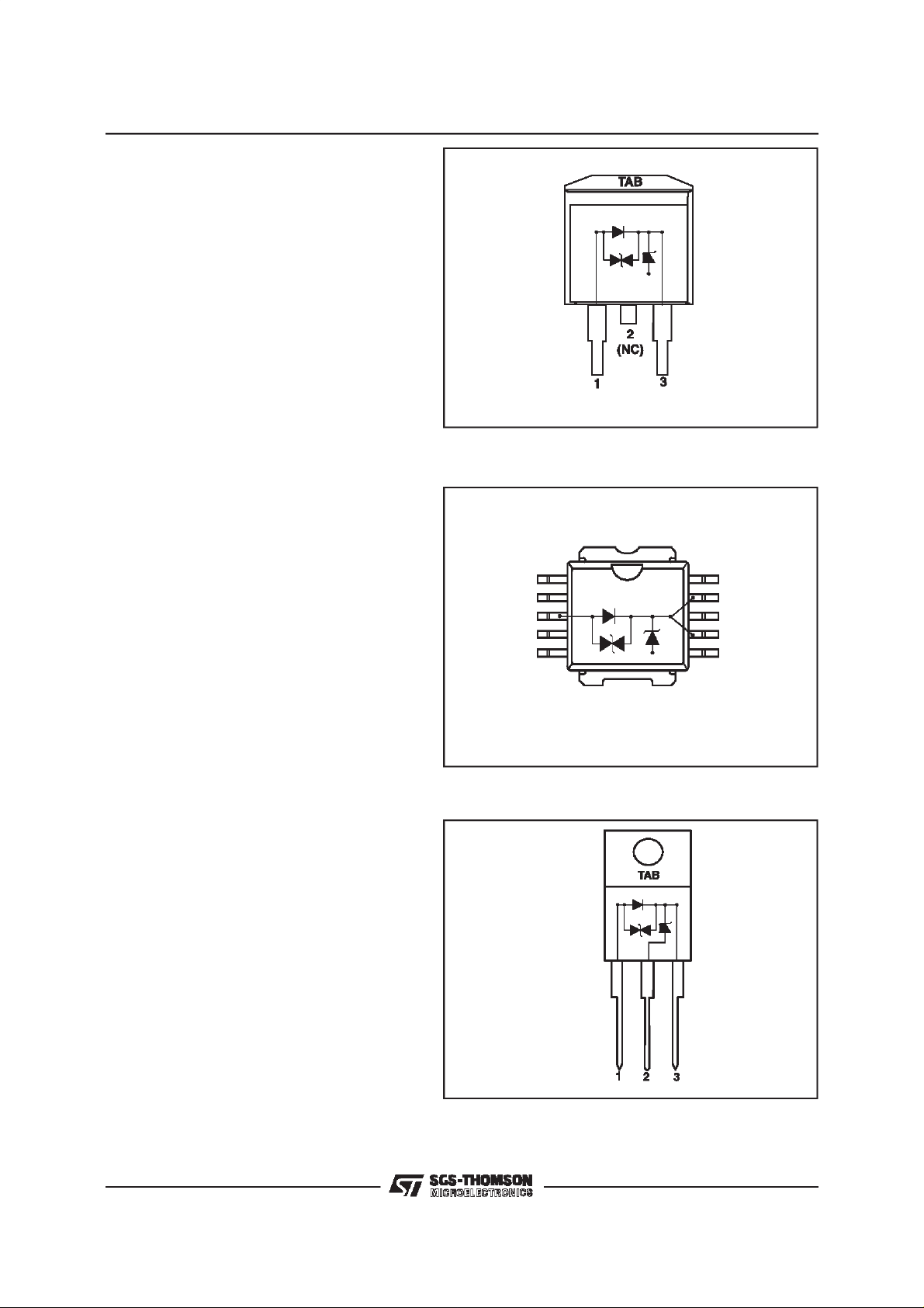
2
PINOUTconfigurationin D
PAK:
-Input (1) : Pin1
-Output (3) : Pin3
-Gnd (2) : Connectedto base Tab
Marking : Logo, datecode, RBO08-40G
PINOUTconfigurationin PowerSO-10:
-Input (1) : Pin3
-Output (3) : Pin7 and9
-Gnd (2) : Connectedto base Tab
Marking : Logo, datecode, RBO08-40M
RBO08-40G / RBO08-40M / RBO08-40T
D1
T2
T1
TAB
Pin 1 (NC)
Pin 2 (NC)
Pin 3 (Input 1)
Pin 4 (NC)
Pin 5 (NC)
Input (1)
D1
Output(3)
T2
T1
Gnd (2)
Tab
Pin 10(NC)
Pin 9 (Ouput 3)
Pin 8 (NC)
Pin 7 (Ouput 3)
Pin 6 (NC)
PINOUTconfigurationin TO220AB:
-Input (1) : Pin1
-Output (3) : Pin3
-GND (2) : Connectedto base Tab
Marking : Logo, datecode, RBO08-40T
TOP VIEW
D1
T2
T1
(TAB)
5/14
Page 6

RBO08-40G / RBO08-40M / RBO08-40T
Fig. 1 : Peak pulse power versus exponential
pulseduration(Tj initial = 85°C).
(kW)
p
P
p
10.0
5.0
2.0
1.0
Transil T 2
0.5
0.2
Diode D1
0.1
1 2 5 10 20 50 100
tp(ms)
Fig. 2-2 : Clamping voltage versus peak pulse
current (Tj initial =85°C).
Exponential waveform tp = 1 ms and tp = 20 µs
(TRANSILT1).
Fig. 2-1 : Clamping voltage versus peak pulse
current (Tj initial = 85°C).
Exponential waveform tp = 40 ms and tp = 1 ms
(TRANSILT2).
VCL(V)
45
40
tp = 40ms
35
tp = 1ms
30
Ipp(A)
25
0.1 0.2 0.5 1.0 5.0 10.0 20.0 50.0
Fig. 3 :
Relative variation of peak pulse power
2.0
versus junction temperature.
VCL(V)
50
45
40
35
tp = 1ms
tp = 20 s
µ
30
Ipp(A)
25
0.1 0.2 0.5 1.0 2.0 5.0 10.0 20.0 50.0 100.0
Ppp[Tj]/Ppp[Tj initial=85°C]
1.20
1.00
0.80
0.60
0.40
0.20
0.00
0 25 50 75 100 125 150 175
Tj initial(°C)
6/14
Page 7

RBO08-40G / RBO08-40M / RBO08-40T
Fig. 4 :
Relative variation of thermal impedance
junctionto caseversuspulse duration.
Zth(j-c)/Rth(j-c)
1.0
0.5
0.2
0.1
1E-3 1E-2 1E-1 1E+0 1E+1
Fig. 5-2 :
Peak forward voltage drop versus peak
tp (s)
forwardcurrent(typical values)- (DIODED1).
V(VFM )
1.6
1.4
1.2
1.0
0.8
0.6
0.4
0.2
0.0
Tj=25°C
Tj=150°C
IFM (A)
0.1 1.0 10.0 20.0
Fig. 5-1 :
Peakforward voltage drop versus peak
forwardcurrent (typicalvalues)- (TRANSILT2).
V(V
FM )
2.0
1.8
1.6
1.4
1.2
Tj=25°C
1.0
0.8
0.6
0.4
0.2
0.0
0.1 1.0 10.0 20.0
Tj=150°C
IFM (A)
Fig.6 : Relative variation of leakage current
versus junction temperature.
ORDERINGINFORMATION
RBO 08 - 40 M
ReversedBattery&
Overvoltageprotection
I
F(AV)
=8A
Package:
M = PowerSO-10
2
PAK
G=D
T =TO220AB
=40V
V
CL
7/14
Page 8

RBO08-40G / RBO08-40M / RBO08-40T
PACKAGEMECHANICAL DATA
2
PAK Plastic
D
A
E
L2
L
L3
A1
B2
B
G
2.0 MIN.
FLATZONE
C2
C
A2
R
V2
DIMENSIONS
REF.
Millimeters Inches
Min. Typ. Max. Min. Typ. Max.
A 4.30 4.60 0.169 0.181
A1 2.49 2.69 0.098 0.106
A2 0.03 0.23 0.001 0.009
D
B 0.70 0.93 0.027 0.037
B2 1.40 0.055
C 0.45 0.60 0.017 0.024
C2 1.21 1.36 0.047 0.054
D 8.95 9.35 0.352 0.368
E 10.00 10.28 0.393 0.405
G 4.88 5.28 0.192 0.208
L 15.00 15.85 0.590 0.624
L2 1.27 1.40 0.050 0.055
L3 1.40 1.75 0.055 0.069
R 0.40 0.016
V2 0° 8° 0° 8°
FOOT-PRINT D
10.30
2
PAK
8.90
16.90
5.08
1.30
3.70
8/14
Page 9

RBO08-40G / RBO08-40M / RBO08-40T
SOLDERINGRECOMMENDATION
The soldering process causes considerable
thermal stress to a semiconductor component.
This has to be minimized to assure a reliable and
extended lifetime of thedevice. The PowerSO-10
package can be exposed to a maximum
temperatureof 260°C for 10 seconds. However a
proper soldering of the package could be done at
215°C for 3 seconds. Any solder temperature
profile should be within these limits. As reflow
techniquesaremost commonin surfacemounting,
typical heating profiles are given in Figure 1,either
for mounting on FR4 or on metal-backed boards.
For each particular board, the appropriate heat
profile has to be adjusted experimentally. The
present proposal is just a starting point. In any
case, the following precautions have to be
considered:
- alwayspreheatthe device
- peak temperatureshould be at least30 °C
higherthanthe melting point of thesolder
alloychosen
Fig. 1 : Typicalreflowsoldering heat profile
-thermalcapacity of thebasesubstrate
Voids pose a difficult reliability problem for large
surface mount devices. Such voids under the
package result in poor thermal contact and the
high thermal resistance leads to component
failures. The PowerSO-10 is designed from
scratch to be solely a surface mount package,
hence symmetry in the x- and y-axis gives the
package excellent weight balance. Moreover, the
PowerSO-10offersthe uniquepossibilityto control
easily the flatness and quality of the soldering
process. Both the top and the bottom soldered
edges of the package are accessible for visual
inspection(soldering meniscus).
Coplanarity between the substrate and the
package can be easily verified. The quality of the
solder joints is very importantfor two reasons : (I)
poor quality solder joints result directly in poor
reliability and (II) solder thickness affects the
thermal resistance significantly. Thus a tight
control of this parameter results in thermally
efficientandreliable solder joints.
Temperature ( C)
250
o
o
245 C
o
215 C
200
Soldering
Cooli ng
150
Epoxy FR4
board
Preheating
100
Metal-backed
50
board
0
0 40 80 120 1 60 200 240 280 320 360
Time (s)
9/14
Page 10

RBO08-40G / RBO08-40M / RBO08-40T
SUBSTRATES AND MOUNTINGINFORMATION
The use of epoxyFR4 boards is quite commonfor
surface mounting techniques,however, their poor
thermal conduction compromisesthe otherwise
outstanding thermal performance of the
PowerSO-10. Some methods to overcome this
limitationare discussedbelow.
One possibility to improve the thermal conduction
is the use of large heat spreader areas at the
copper layer of the PC board. This leads to a
reductionof thermal resistance to 35 °C for 6 cm
of theboard heatsink(see fig. 2).
Use of copper-filledthroughholes on conventional
FR4 techniqueswillincreasethe metallizationand
Fig.2 :
Mountingon epoxyFR4head dissipationbyextendingthe area of thecopperlayer
Copper foil
decrease thermal resistance accordingly. Using
a configurationwith 16holesunderthe spreaderof
the packagewitha pitchof1.8 mm and a diameter
of 0.7 mm, the thermal resistance (junction heatsink) can be reduced to 12°C/W (see fig. 3).
Besidethe thermaladvantage,thissolution allows
multi-layer boards to be used. However, a
drawback of this traditional material prevents its
use in very high power, high current circuits. For
instance, it is not advisable to surface mount
devices with currents greater than 10 A on FR4
2
boards. A Power Mosfet or Schottky diode in a
surfacemount power packagecan handleup to
around50 A ifbetter substratesare used.
FR4 board
Fig. 3 :
10/14
Mountingon epoxy FR4 byusingcopper-filledthrough holesfor heattransfer
Copperfoil
heattransferheatsink
FR4board
Page 11

RBO08-40G / RBO08-40M / RBO08-40T
A new technology available today is IMS - an
Insulated Metallic Substrate. This offers greatly
enhanced thermal characteristics for surface
mount components.IMS is a substrateconsisting
of threedifferentlayers,(I)thebasematerialwhich
is availableas an aluminiumor a copper plate,(II)
a thermal conductive dielectrical layer and (III) a
copper foil, which can be etched as a circuitlayer.
Using this materiala thermalresistance of 8°C/W
with 40 cm
2
of board floating in air is achievable
(seefig.4).If evenhigherpoweristo bedissipated
an externalheatsinkcould be applied which leads
to an R
that R
(j-a) of 3.5°C/W (see Fig. 5), assuming
th
(heatsink-air) is equal to R
th
(junction-heatsink). This is commonly applied in
practice, leading to reasonable heatsink
dimensions. Often power devices are defined by
Fig.4 : Mountingon metalbacked board
Copper foil
Insulation
consideringthe maximumjunction temperature of
the device. In practice , however, this is far from
being exploited. A summary of various power
managementcapabilities is made in table 1 based
on a reasonabledeltaT of70°Cjunctionto air.
The PowerSO-1 0 concept also represents a n
attractive alternative to C.O.B. techniques.
PowerSO-10 offers devices fully tested at low
and high temperature. Mounting is simple - only
conventionalSMT is required- enablingthe users
togetrid ofbond wire problemsand the problemto
controlthe hightemperaturesoftsolderingaswell.
An optimized thermal managementis guaranteed
th
through PowerSO-10 as the power chips must in
any case be mounted on heat spreaders before
beingmountedonto the substrate.
Fig. 5 :
Mounting on metal backed board with an
externalheatsinkapplied
Copper foil
FR4board
Alumini um
Aluminium
heatsink
TABLE1
PowerSo-10packagemountedon Rth(j-a) PDiss
1.FR4usingtherecommendedpad-layout
2
2.FR4withheatsinkon board (6cm
)35°C/W 2.0 W
50 °C/W 1.5 W
3.FR4withcopper-filledthroughholesand externalheatsink applied 12 °C/W 5.8W
4. IMS floating in air (40 cm
5. IMS with externalheatsinkapplied
2
)8°C/W 8.8 W
3.5 °C/W 20W
11/14
Page 12

RBO08-40G / RBO08-40M / RBO08-40T
PACKAGEMECHANICAL DATA
B
H
A1
Q
0.10A B
E3 E1
SEATING
PLANE
A
C
10
E
1
eB
0.25 M
6
E2
5
DETAIL”A”
D
h
D1
A
F
SEATING
PLANE
A1
L
DETAIL ”A”
a
E4
DIMENSIONS
REF.
Millimeters Inches
Min. Typ. Max. Min. Typ. Max.
A 3.35 3.65 0.131 0.143
A1 0.00 0.10 0.00 0.0039
B 0.40 0.60 0.0157 0.0236
C 0.35 0.55 0.0137 0.0217
D 9.40 9.60 0.370 0.378
D1 7.40 7.60 0.291 0.299
E 9.30 9.50 0.366 0.374
E1 7.20 7.40 0.283 0.291
E2 7.20 7.60 0.283 0.299
12/14
DIMENSIONS
REF.
Millimeters Inches
Min. Typ. Max. Min. Typ. Max.
E3 6.10 6.35 0.240 0.250
E4 5.90 6.10 0.232 0.240
e 1.27 0.05
F 1.25 1.35 0.0492 0.0531
H 13.80 14.40 0.543 0.567
h 0.50 0.019
L 1.20 1.80 0.0472 0.0708
Q 1.70 0.067
a0° 8°0° 8°
Page 13

RBO08-40G / RBO08-40M / RBO08-40T
FOOTPRINT
MOUNTINGPAD LAYOUT
RECOMMENDED
Dimensionsin millimeters Dimensionsin millimeters
HEADERSHAPE
SHIPPINGTUBE
C
B
A
Surfacemount film taping: contactsalesoffice
A
B
C
Lengthtube
Quantityper tube
DIMENSIONS(mm)
TYP
18
12
0,8
532
50
13/14
Page 14

RBO08-40G / RBO08-40M / RBO08-40T
PACKAGEMECHANICALDATA
TO220AB Plastic
DIMENSIONS
REF.
Millimeters Inches
Min. Max. Min. Max.
A 14.23 15.87 0.560 0.625
a1 4.50 0.177
a2 12.70 14.70 0.500 0.579
B 10.20 10.45 0.402 0.411
b1 0.64 0.96 0.025 0.038
b2 1.15 1.39 0.045 0.055
C 4.48 4.82 0.176 0.190
c1 0.35 0.65 0.020 0.026
c2 2.10 2.70 0.083 0.106
e 2.29 2.79 0.090 0.110
F 5.85 6.85 0.230 0.270
I 3.55 4.00 0.140 0.157
L 2.54 3.00 0.100 0.118
l2 1.45 1.75 0.057 0.069
l3 0.80 1.20 0.031 0.047
Information furnished is believed to be accurate and reliable. However, SGS-THOMSON Microelectronics assumes no responsibility for the
consequences of use of such information nor for any infringement of patents or other rights of thirdparties which may result from its use. No
license is grantedby implication or otherwise under any patentor patent rights of SGS-THOMSON Microelectronics.Specifications mentioned
in thispublication are subjectto change without notice. This publicationsupersedes and replaces all informationpreviously supplied.
SGS-THOMSONMicroelectronics productsare notauthorized for use as criticalcomponents in lifesupport devices or systems withoutexpress
written approval of SGS-THOMSON Microelectronics.
1997 SGS-THOMSON Microelectronics -Printed in Italy - All rights reserved.
SGS-THOMSON MicroelectronicsGROUP OF COMPANIES
Australia- Brazil - Canada - China - France - Germany - Italy - Japan - Korea - Malaysia - Malta - Morocco
The Netherlands - Singapore- Spain -Sweden - Switzerland - Taiwan - Thailand - United Kingdom -U.S.A.
14/14
 Loading...