

Page 1
CYStech Electronics Corp.
0.5A surface mount Schottky diode
RB0540S2
Features
• High current capability, low forward voltage drop
• High surge current capability
• Guardring for over voltage protection
• Low power loss, high efficiency
• Ultra high-speed switching
• Low profile surface mounted package in order to minimize board space
Mechanical data
•Case : Molded plastic, SC-76/SOD323
•Epoxy : UL94-V0 rated flame retardant
•Terminals : Plated terminals, solderable per MIL-STD-750 method 2026
•Polarity : Indicated by cathode band
•Mounting position : Any
•Weight : approx. 0.0045 gram
Spec. No. : C291S2
Issued Date : 2008.12.15
Revised Date : 2013.11.28
Page No. : 1/6
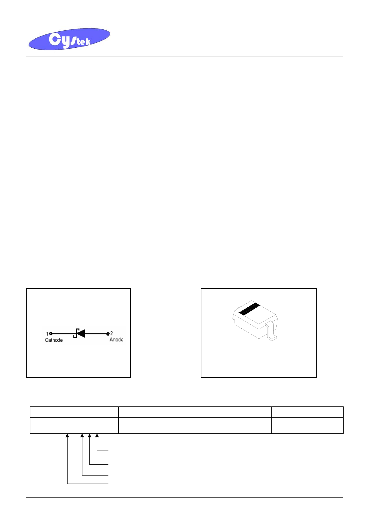
Symbol Outline
RB0540S2
Ordering Information
Device Package Shipping
RB0540S2-0-T1-G
(Pb-free lead plating and halogen-free package)
SOD-323
Environment friendly grade : S for RoHS compliant products, G for RoHS compliant and
green compound products
Packing spec, T1 : 3000 pcs / tape & reel, 7” reel
Product rank, zero for no rank products
Product name
SOD-323
2 (Anode)
3000 pcs / tape & reel
RB0540S2 CYStek Product Specification
Page 2

CYStech Electronics Corp.
Absolute Maximum Ratings (TA=25℃, unless otherwise noted)
Spec. No. : C291S2
Issued Date : 2008.12.15
Revised Date : 2013.11.28
Page No. : 2/6
Parameters Conditions
Repetitive peak reverse voltage
RMS voltage
Symbol Min Typ Max Units
V
V
Continuous reverse voltage
I
Forward rectified current
Forward surge current
Thermal resistance Junction to Ambient
Storage temperature range
Operating junction temperature range
Single phase half wave, 60Hz
@T
=25°C
J
8.3ms single half sine-wave
superimposed on rated load
(JEDEC method)
Tstg
Tj
I
Characteristics
Characteristic Symbol Condition Min. Typ Max. Unit
(TA=25°C)
RRM
RMS
VR 40 V
O
F(AV)
I
FSM
R
JA
θ
40 V
28 V
0.5
1
15 A
90
-65 175
-55 125
A
°C/W
°C
°C
Forward Voltage
VR IR=600μA
VF 1 IF=100mA -
VF 2 IF=500mA -
IR 1 VR=20V -
Reverse Leakage Current
IR 2 VR=40V -
R 3
I
VR=40V, TA=75°C
Capacitance Between Terminals CT VR=4V, f=1MHz -
40
-
-
-
-
-
-
-
18.3
- V
370
mV
500
100 μA
500 μA
10 mA
- pF
RB0540S2 CYStek Product Specification
Page 3
CYStech Electronics Corp.
Characteristic Curves
Spec. No. : C291S2
Issued Date : 2008.12.15
Revised Date : 2013.11.28
Page No. : 3/6
Forward Current Derating Curve
0.6
0.5
0.4
0.3
0.2
resistive or inductive load
0.1
Average Forward Current---Io(A)
0
0 25 50 75 100 125 150 175
Ambient Temperature---T
A
Forward Current vs Forward Voltage
1000
(mA)
F
100
Tj=125℃
Tj=75℃
(℃)
Maximum Non-Repetitive Forward Surge Current
15
(A)
12
FSM
9
6
3
Peak Forward Surge Current---I
0
1 10 100
Tj=25℃, 8. 3ms Single Half Sine
Wave, JEDEC method
Number of Cycles at 60Hz
Junction Capacitance vs Reverse Voltage
100
(pF)
J
10
Instantane ous Forward Current---I
1
0 0.2 0.4 0.6
Forward Volt age ---V
Tj=25℃
Pulse width=300μs,
1% Duty cycle
(V)
F
Reverse Leakage Current vs Reverse Voltage
10000
(μA)
R
1000
Tj=75℃
100
Reverse Leakage Current---I
10
0 20 40 60 80 100 120 140
Percent of Rated Peak
Tj=25℃
Reverse Voltage---(%)
Tj=25℃, f=1. 0MHz
Junction Capacitance---C
10
0.1 1 10
Reverse Voltage---V
(V)
R
RB0540S2 CYStek Product Specification
Page 4

Reel Dimension
CYStech Electronics Corp.
Spec. No. : C291S2
Issued Date : 2008.12.15
Revised Date : 2013.11.28
Page No. : 4/6
Carrier Tape Dimension
RB0540S2 CYStek Product Specification
Page 5

CYStech Electronics Corp.
Recommended wave soldering condition
Product Peak Temperature Soldering Time
Spec. No. : C291S2
Issued Date : 2008.12.15
Revised Date : 2013.11.28
Page No. : 5/6
Pb-free devices
260 +0/-5 °C
Recommended temperature profile for IR reflow
5 +1/-1 seconds
Profile feature Sn-Pb eutectic Assembly
Average ramp-up rate
(Tsmax to Tp)
Preheat
−Temperature Min(TS min)
−Temperature Max(TS max)
−Time(ts min to ts max)
Time maintained above:
−Temperature (TL)
− Time (tL)
Peak Temperature(TP)
Time within 5°C of actual peak
temperature(tp)
Ramp down rate
Time 25 °C to peak temperature
Note : All temperatures refer to topside of the package, measured on the package body surface.
3°C/second max. 3°C/second max.
100°C
150°C
60-120 seconds
183°C
60-150 seconds
240 +0/-5 °C 260 +0/-5 °C
10-30 seconds 20-40 seconds
6°C/second max. 6°C/second max.
6 minutes max. 8 minutes max.
Pb-free Assembly
150°C
200°C
60-180 seconds
217°C
60-150 seconds
RB0540S2 CYStek Product Specification
Page 6

SOD-323 Dimension
K
A
CYStech Electronics Corp.
Spec. No. : C291S2
Issued Date : 2008.12.15
Revised Date : 2013.11.28
Page No. : 6/6
Marking:
5 H
C
2
B
J
Millimeters Inches Millimeters
DIM
C
E
Min. Max. Min. Max.
Style: Pin 1.Cathode 2.Anode
2-Lead SOD-323 Plastic Surface
Mounted Package,
CYStek Package Code: S2
*: Typical
D
DIM
1
H
Inches
Min. Max. Min. Max.
A 0.0630 0.0709 1.60 1.80 E 0.0060 REF 0.15 REF
B 0.0453 0.0531 1.15 1.35 H 0.0000 0.0040 0.00 0.10
C 0.0315 0.0394 0.80 1.00 J 0.0035 0.0070 0.089 0.177
D 0.0098 0.0157 0.25 0.40 K 0.0906 0.1063 2.30 2.70
Notes: 1.Controlling dimension : millimeters.
Material:
• Lead: Pure tin plated.
• Mold Compound: Epoxy resin family, flammability solid burning class: UL94V-0.
2.Lead thickness specified per L/F drawing with solder plating.
3.If there is any question with packing specification or packing method, please contact your local CYStek sales office.
Important Notice:
• All rights are reserved. Reproduction in whole or in part is prohibited without the prior written approval of CYStek.
• CYStek reserves the right to make changes to its products without notice.
• CYStek semiconductor products are not warranted to be suitable for use in Life-Support Applications, or systems.
• CYStek assumes no liability for any consequence of customer product design, infringement of patents, or application assistance.
RB0540S2 CYStek Product Specification
Page 7

 Loading...