

Page 1
Enhanced Quadruple Mode PWM Flyback Controller
GND COMP PRO
CSVDDGATE
4
2 3
56
R7732
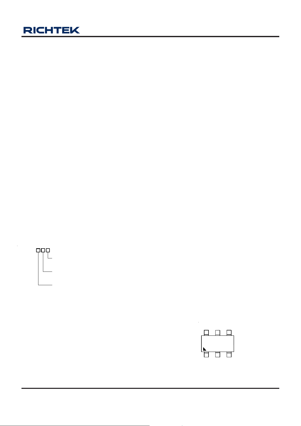
Package Type
E : SOT-23-6
Lead Plating System
G : Green (Halogen Free and Pb Free)
R7732 Version (Refer to Version Table)
R7732
General Description
R7732 series is the successor of R7730/1 and fully
compatible with most of SOT-23-6 product so far in the
market. It's an enhanced, high-performance and current
mode PWM controller. It focuses on "easy to design" in
different applications and it will save both design effort and
external components.
Besides the general features shown in the Features
section, R7732 covers wide protection options, such as
internal Over Load Protection (OLP) and Over Voltage
Protection (OVP) to eliminate the external protection
circuits. Moreover, it also features Secondary Rectifier
Short Protection (SRSP) and CS pin open protection. This
protection will make the PSU design for reliability and safety
easier.
R7732 is designed for power supply such as NB adaptor
which is a very cost effective and compact design. The
precise external OVP and Over Temperature Protection
(OTP) can be implemented by very simple circuit. The
start-up resistors can also be replaced by bleeding
resistors to save power loss and component count.
Features
ll
l UVLO 9V/14V
ll
ll
l Soft-Start Function
ll
ll
l Current Mode Control
ll
ll
l Built-in Slope Compensation
ll
ll
l Internal Leading Edge Blanking
ll
ll
l PWM Quadruple Mode for Green-Mode
ll
ll
l Excellent Green Power Performance
ll
ll
l Cycle-by-Cycle Current Limit
ll
ll
l Internal Over Voltage Protection
ll
ll
l Internal Over Load Protection
ll
ll
l Secondary Rectifier Short Protection
ll
ll
l Opto-Coupler Short Protection
ll
ll
l Feedback Open-Loop Protection
ll
ll
l CS Pin Open Protection
ll
ll
l Built-in Jittering Frequency
ll
ll
l Built-in PRO Pin for External Arbitrary OVP/OTP
ll
ll
l Soft Driving for EMI Noise
ll
ll
l High Noise Immunity
ll
ll
l RoHS Compliant and Halogen Free
ll
Application
Ordering Information
Note :
Richtek products are :
} RoHS compliant and compatible with the current require-
ments of IPC/JEDEC J-STD-020.
} Suitable for use in SnPb or Pb-free soldering processes.
R7732-00 May 2011
ll
l Switching AC/DC Adaptor and Battery Charger
ll
ll
l Printer Power Supply
ll
ll
l DVD Open Frame Power Supply
ll
ll
l Set-Top Box (STB)
ll
ll
l ATX Standby Power
ll
ll
l TV/Monitor Standby Power
ll
ll
l PC Peripherals
ll
ll
l NB Adaptor
ll
Pin Configurations
(TOP VIEW)
SOT-23-6
www.richtek.com
1
Page 2
R7732
AC Mains
(90V to 265V)
PRO
COMP
GND
GATE
CS
R7732
VDD
+
+
Vo+
Vo-
5
6
2
1
4
#
# See Application Information
3
NTC
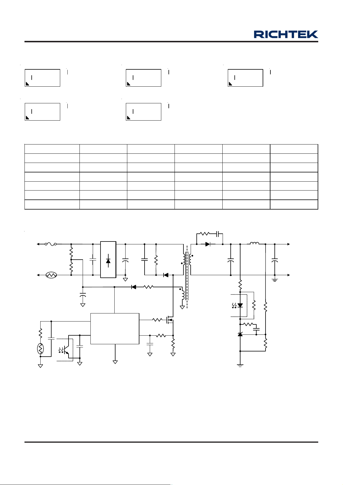
Version R7732G R7732R R7732L R7732A R7732H
Frequency 65kHz 65kHz 65kHz 65kHz 100kHz
OLP Delay Time 56ms 56ms 56ms 28ms 36ms
Internal OVP(27V) Auto Recovery Auto Recovery
Latch Latch Auto Recovery
OLP & SRSP Auto Recovery Auto Recovery Auto Recovery
Latch Auto Recovery
PRO Pin High Latch Auto Recovery
Latch Latch Auto Recovery
PRO Pin Low Auto Recovery
Latch Latch Latch Latch
F0=DNN
F2=DNN
F3=DNN
F4=DNN
F6=DNN
Marking Information
R7732GGE
F0= : Product Code
DNN : Date Code
R7732HGE
F4= : Product Code
DNN : Date Code
R7732 Version Table
Typical Application Circuit
R7732LGE
R7732RGE
F2= : Product Code
DNN : Date Code
F6= : Product Code
DNN : Date Code
R7732AGE
F3= : Product Code
DNN : Date Code
www.richtek.com
2
R7732-00 May 2011
Page 3
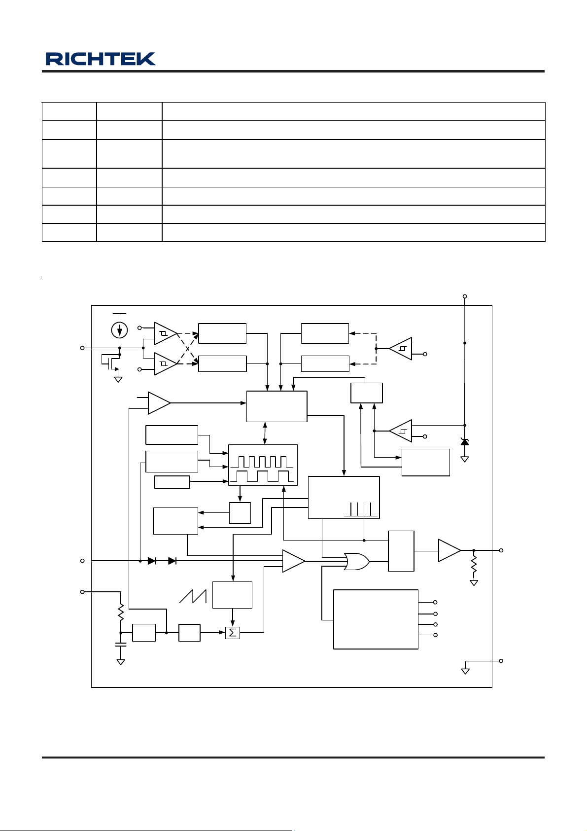
Pin No. Pin Name Pin Function
1 GND Ground.
2 COMP
Voltage Feedback Pin. By connecting an opto-
coupler to close control loop and achieve
the regulation.
3 PRO For External Arbitrary OVP or OTP.
4 CS Primary Current Sense Pin.
5 VDD Power Supply Pin.
6 GATE Gate Drive Output to drive the external MOSFET.
Functional Pin Description
Counter
VDD
GATE
LEB
R
S
Q
SS
X3
Slope
Ramp
V
COMP
V
BURH
V
BURL
PWM
Comparator
Shutdown
Logic
COMP Open
Sensing
Brownout
Sensing
Dmax
Oscillator
POR
27V
Bias &
Bandgap
UVLO
OVP
9V/14V
OLP
Constant
Power
Soft Driver
+
-
+
-
+
-
-
+
-
1.7V
Secondary Rectifier Short
& CS Open Protection
COMP
CS
PRO
Quadruple Mode
+
-
+
-
Latch
V
L_TH
V
H_TH
V
DD
I
BIAS
Auto
Recovery
Latch
Auto
Recovery
GND
Function Block Diagram
R7732
R7732-00 May 2011
www.richtek.com
3
Page 4
R7732
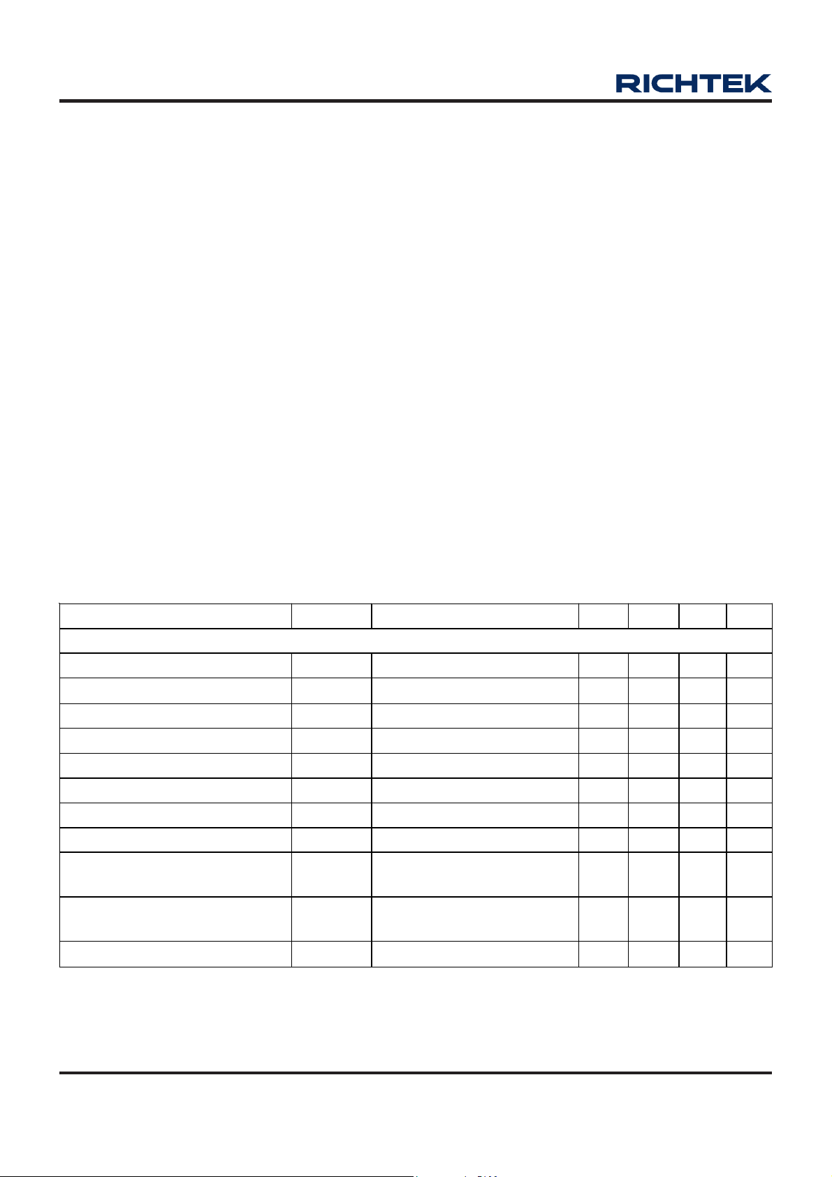
Parameter Symbol Test Conditions Min Typ Max Unit
VDD Section
VDD Over Voltage Protection Level V
OVP
26 27 28 V
VDD Zener Clamp VZ 29 -- - - V
On Threshold Voltage V
TH_ON
13 14 15 V
Off Threshold Voltage V
TH_OFF
8.5 9 9.5 V
VDD Holdup Mode Entry Point V
DD_LOW
V
COMP
<1.6V -- 10 - - V
VDD Holdup Mode Ending Point V
DD_HIGH
V
COMP
<1.6V -- 10.5
- - V
Latch-off Voltage VLH -- 14 - - V
Latched Reset Voltage V
LH_RST
-- 9 - - V
Start-up Current I
DD_ST
VDD = V
TH_ON –
0.2V,
TA= -40ºC to 100ºC (N ote 5)
-- 20 35 µA
Operating Supply Current I
DD_OP
VDD= 15V, V
COMP
= 2.5V,
GATE pin open
-- 1.3 2.2 mA
Latch-off Operating Current I
DD_LH
TA= -40ºC to 100ºC (Note 5)
-- - - 40 µA
Absolute Maximum Ratings (Note 1)
l Supply Input Voltage, V
l GATE Pin -------------------------------------------------------------------------------------------------------------- −0.3V to 16.5V
l PRO, COMP, CS Pin ----------------------------------------------------------------------------------------------- −0.3V to 6.5V
l I
----------------------------------------------------------------------------------------------------------------------- 10mA
DD
l Power Dissipation, P
----------------------------------------------------------------------------------------- −0.3V to 30V
DD
@ T
= 25°C
D
A
SOT-23-6-------------------------------------------------------------------------------------------------------------- 0.4W
l Package Thermal Resistance (Note 2)
SOT-23-6, θJA-------------------------------------------------------------------------------------------------------- 250°C/W
l Junction Temperature ----------------------------------------------------------------------------------------------- 150°C
l Lead Temperature (Soldering, 10 sec.) ------------------------------------------------------------------------- 260°C
l Storage Temperature Range --------------------------------------------------------------------------------------- −65°C to 150°C
l ESD Susceptibility (Note 3)
HBM (Human Body Mode) ----------------------------------------------------------------------------------------- 3kV
MM (Machine Mode) ------------------------------------------------------------------------------------------------ 250V
Recommended Operating Conditions (Note 4)
l Supply Input Voltage, V
l Junction Temperature Range -------------------------------------------------------------------------------------- −40°C to 125°C
l Ambient Temperature Range -------------------------------------------------------------------------------------- −40°C to 85°C
----------------------------------------------------------------------------------------- 12V to 25V
DD
Electrical Characteristics
(V
= 15V, T
DD
= 25°C, unless otherwise specified)
A
To be continued
www.richtek.com
R7732-00 May 2011
4
Page 5
R7732
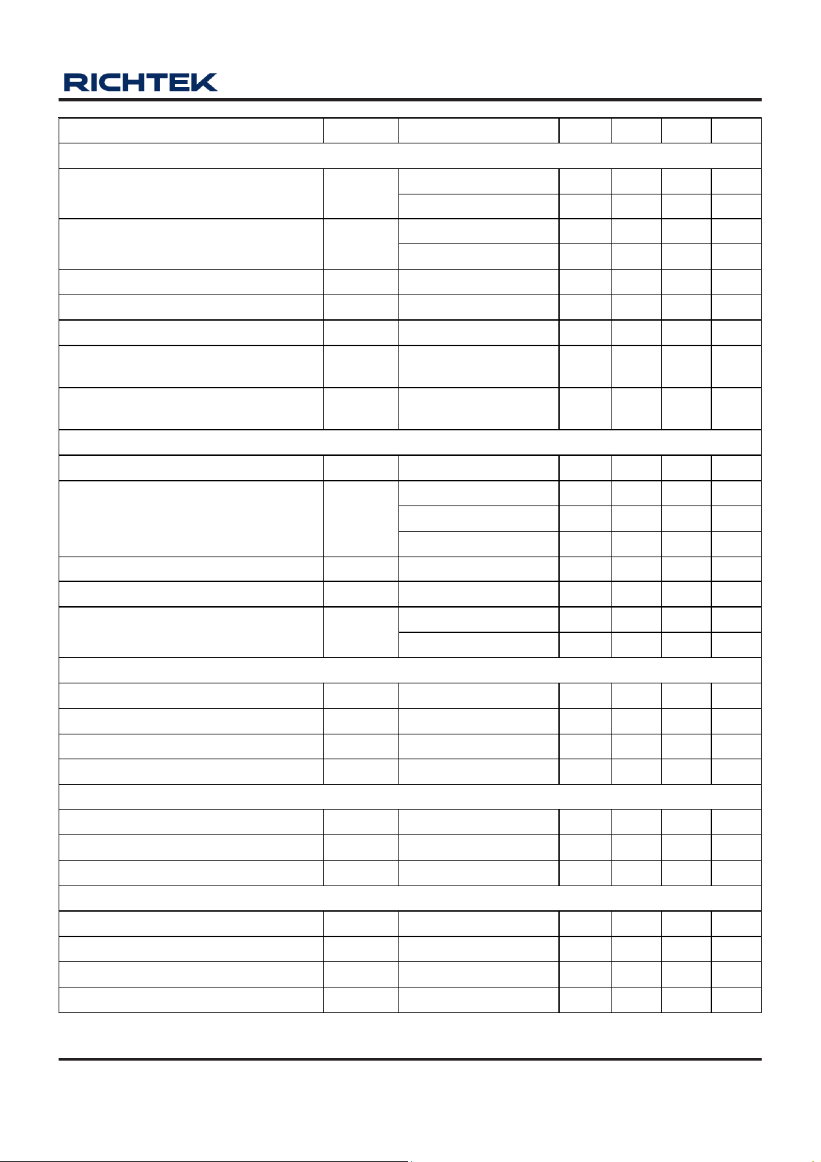
Parameter Symbol
Test Conditions Min Typ Max Unit
Oscillator Section
R7732G/R/L/A 60 65 70 kHz
Normal PWM Frequency f
OSC
R7732H 92 100 108 kHz
R7732G/R/L/A 18 22 - - kHz
Frequency Reduction Mode Minimum
Frequency
f
FR_MIN
R7732H -- 25 - - kHz
Maximum Duty Cycle DCY
MAX
70 75 80 %
PWM Frequency Jitter Range △f -- ±6
- - %
PWM Frequency Jitter Period T
JIT
For 65kHz -- 4 - - ms
Frequency Variation Versus
VDD Deviation
fDV VDD= 12V to 25V -- - - 2 %
Frequency Variation Versus
Temperature Deviation
fDT
TA= -30°C to 105°C
(Note 5)
-- - - 5 %
COMP Input Section
Open-Loop Voltage V
COMP_OP
COMP pin open 5.5 5.75
6 V
R7732G/R/L -- 56 - - ms
R7732A - - 28 - - ms COMP Open-Loop Protection Delay Time T
OLP
R7732H -- 36 - - ms
Short Circuit Current
I
ZERO
V
COMP
= 0V
-- 1.2 2.2 mA
Frequency Reduction Mode Entry Voltage
V
FR _ET
-- 3 - - V
R7732G/R/L/A -- 2.9 - - V
Frequency Reduction Mode Ending
Voltage
V
FR _ED
R7732H -- 2.8 - - V
Current-Sense Section
Initial Peak Current Limitation Offset V
CS_TH
0.68 0.7 0.72
V
Leading Edge Blanking Time T
LEB
(Note 6) 150 250 350 ns
Internal Propagation Delay Time TPD (Note 6) - - 100 - - ns
Minimum On Time T
ON_MIN
250 350 450 ns
GATE Section
Rising Time TR VDD= 15V, CL= 1nF -- 125 - - ns
Falling Time TF VDD= 15V, CL= 1nF -- 40 - - ns
GATE Output Clamping Voltage V
CLAMP
VDD= 25V -- 14 - - V
PRO Interface Section
Pull Low Threshold V
L_TH
0.47 0.5 0.53
V
Pull High Threshold V
H_TH
3.5 3.8 4.1 V
Internal Bias Current I
BIAS
90 100 110 µA
Pull High Sinking Current I
SINK
(Note 7) - - -- 1.2 mA
R7732-00 May 2011
www.richtek.com
5
Page 6

R7732
Note 1. Stresses listed as the above "Absolute Maximum Ratings" may cause permanent damage to the device. These are for
stress ratings. Functional operation of the device at these or any other conditions beyond those indicated in the
operational sections of the specifications is not implied. Exposure to absolute maximum rating conditions for extended
periods may remain possibility to affect device reliability.
Note 2. θ
Note 3. Devices are ESD sensitive. Handling precaution is recommended.
Note 4. The device is not guaranteed to function outside its operating conditions.
Note 5. Guaranteed by design.
Note 6. Leading edge blanking time and internal propagation delay time are guaranteed by design.
Note 7. The sourcing current of PRO pin must be limited below 5mA. Otherwise it may cause permanent damage to the device.
is measured in natural convection at T
JA
JEDEC 51-3 thermal measurement standard.
= 25°C on a low effective single layer thermal conductivity test board of
A
www.richtek.com
6
R7732-00 May 2011
Page 7
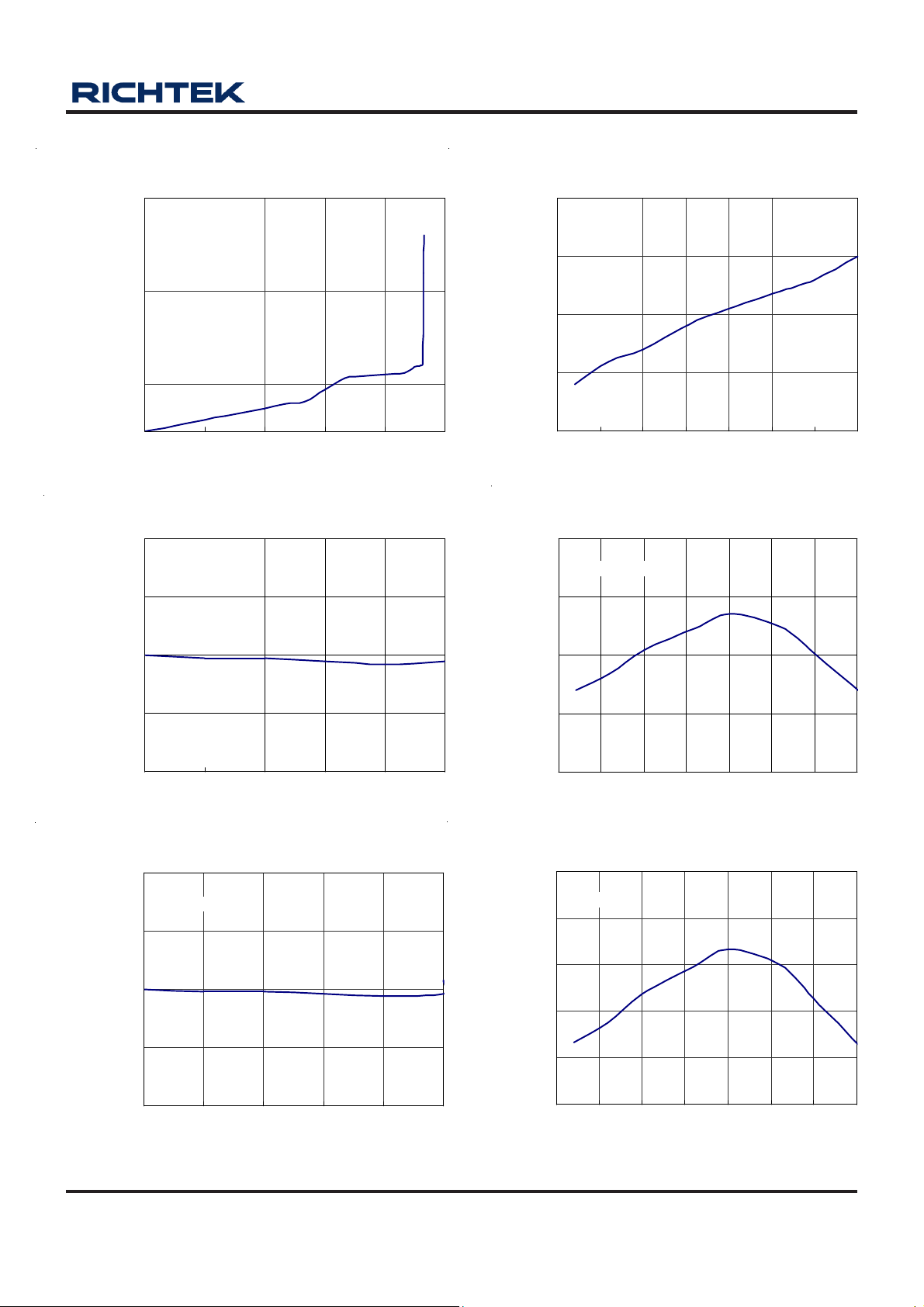
Typical Operating Characteristics
I
DD_ST
vs. V
DD
0
5
10
15
20
25
0 3 6 9 12 15
VDD (V)
I
DD_ST
(µA)
I
DD_ST
vs. Temperature
10
15
20
25
30
-50 -25 0 25 50 75 100 125
Temperature
I
DD_ST
(µA)
f
OSC
vs. V
DD
63
64
65
66
67
10 13 16 19 22 25
VDD (V)
f
OSC
(kHz)
f
OSC
vs. V
DD
96
98
100
102
104
10 13 16 19 22 25
VDD (V)
f
OSC
(kHz)
f
OSC
vs. Temperature
60
62
64
66
68
-50 -25 0 25 50 75 100 125
Temperature
f
OSC
(kHz)
f
OSC
vs. Temperature
94
96
98
100
102
104
-50 -25 0 25 50 75 100 125
Temperature
f
OSC
(kHz)
T
= 25°C
A
R7732
(°C)
R7732G/R/L/A
R7732H
R7732G/R/L/A
(°C)
R7732H
R7732-00 May 2011
(°C)
www.richtek.com
7
Page 8
R7732
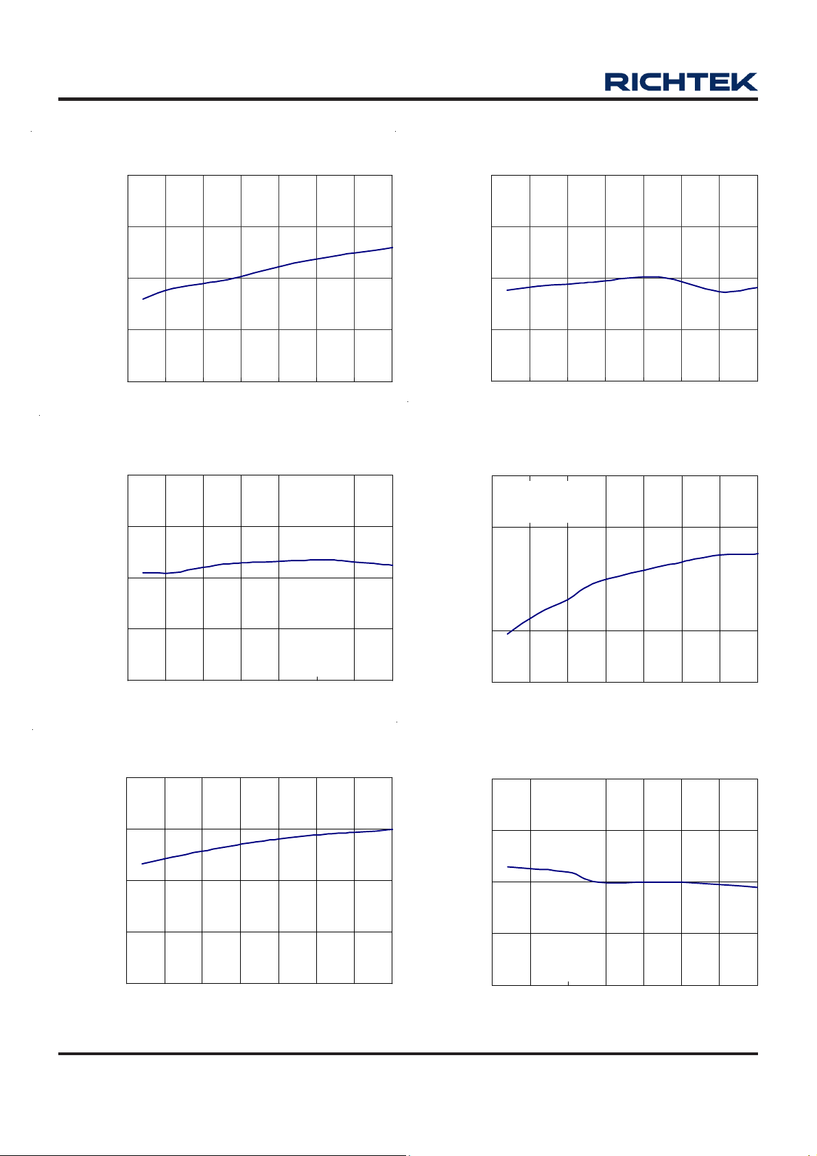
V
TH_ON
vs. Temperature
12
13
14
15
16
-50 -25 0 25 50 75 100 125
Temperature
V
TH_ON
(V)
V
TH_OFF
vs. Temperature
8.0
8.5
9.0
9.5
10.0
-50 -25 0 25 50 75 100 125
Temperature
V
TH_OFF
(V)
f
FR_MIN
vs. Temperature
10
15
20
25
30
-50 -25 0 25 50 75 100 125
Temperature
f
FR_MIN
(kHz)
I
DD_OP
vs. Temperature
1.0
1.2
1.4
1.6
1.8
-50 -25 0 25 50 75 100 125
Temperature
I
DD_OP
(mA)
V
OVP
vs. Temperature
25
26
27
28
29
-50 -25 0 25 50 75 100 125
Temperature
V
OVP
(V)
V
COMP_OP
vs. Temperature
5.2
5.4
5.6
5.8
6
-50 -25 0 25 50 75 100 125
Temperature
V
COMP_OP
(V)
(°C)
(°C)
V
= 15V,
DD
V
= 2.5V,
COMP
GATE Pin Open
(°C)
(°C)
www.richtek.com
8
(°C)
(°C)
R7732-00 May 2011
Page 9
R7732
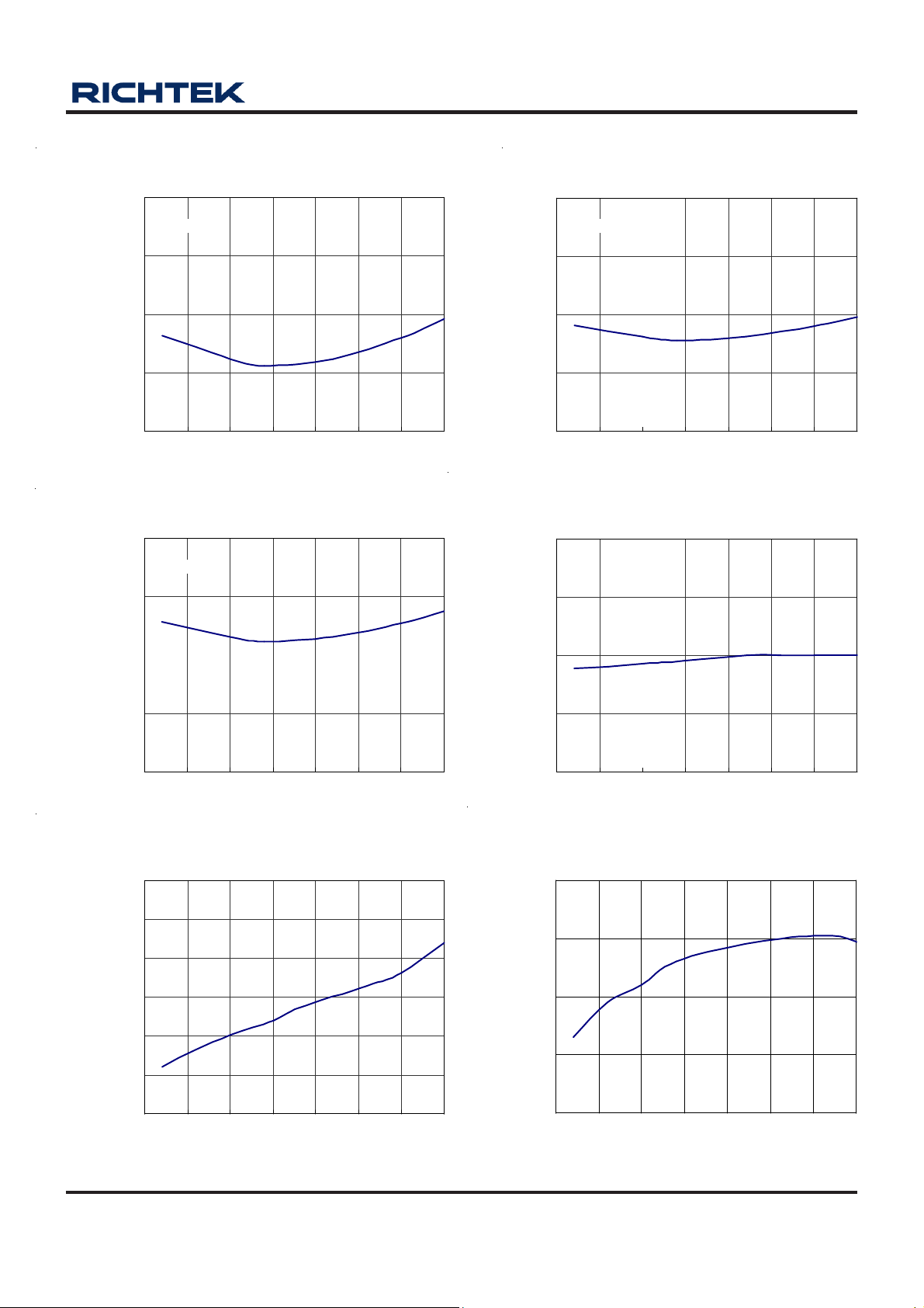
T
OLP
vs. Temperature
50
55
60
65
70
-50 -25 0 25 50 75 100 125
Temperature
T
OLP
(ms)
T
OLP
vs. Temperature
20
25
30
35
40
-50 -25 0 25 50 75 100 125
Temperature
T
OLP
(ms)
T
OLP
vs. Temperature
25
30
35
40
45
-50 -25 0 25 50 75 100 125
Temperature
T
OLP
(ms)
V
CS_TH
vs. Temperature
0.60
0.65
0.70
0.75
0.80
-50 -25 0 25 50 75 100 125
Temperature
V
CS_TH
(V)
I
DD_LH
vs. Temperature
10
15
20
25
30
35
40
-50 -25 0 25 50 75 100 125
Temperature
I
DD_LH
(µA)
I
BIAS
vs. Temperature
70
80
90
100
110
-50 -25 0 25 50 75 100 125
Temperature
I
BIAS
(µA)
R7732G/R/L
R7732H
(°C)
R7732A
(°C)
R7732-00 May 2011
(°C)
(°C)
(°C)
(°C)
www.richtek.com
9
Page 10
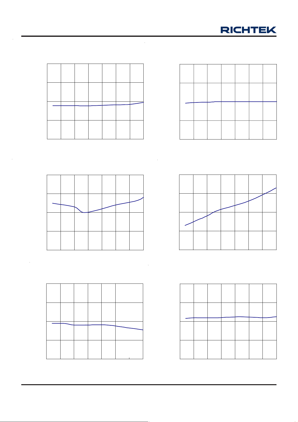
R7732
V
H_TH
vs. Temperature
2
3
4
5
6
-50 -25 0 25 50 75 100 125
Temperature
V
H_TH
(V)
V
L_TH
vs. Temperature
0.40
0.45
0.50
0.55
0.60
-50 -25 0 25 50 75 100 125
Temperature
V
L_TH
(V)
TR vs. Temperature
100
110
120
130
140
-50 -25 0 25 50 75 100 125
Temperature
T
R
(ns)
TF vs. Temperature
20
30
40
50
60
-50 -25 0 25 50 75 100 125
Temperature
T
F
(ns)
V
CLAMP
vs. Temperature
10
12
14
16
18
-50 -25 0 25 50 75 100 125
Temperature
V
CLAMP
(V)
DCY
MAX
vs. Temperature
70
72
74
76
78
-50 -25 0 25 50 75 100 125
Temperature
DCY
MAX
(%)
(°C)
(°C)
(°C)
(°C)
www.richtek.com
10
(°C)
(°C)
R7732-00 May 2011
Page 11
Application Information
f
OSC
f
FR_MIN
V
FR_ET
Freq.
V
COMP
V
FR_ED
Load
V
DD
V
DD_HIGH
V
DD_LOW
Normal
Operation
Frequency
Reduction
Mode
Burst
Mode
VDD
Holdup Mode
V
COMP
V
BURH
V
BURL
GATE
PWM Quadruple Mode
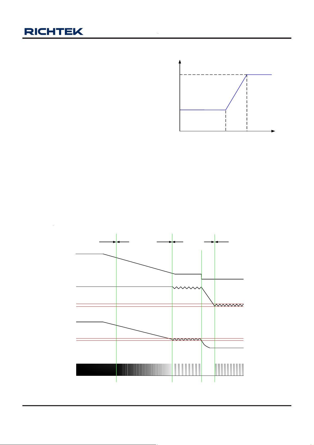
R7732 applies quadruple mode for improving efficiency at
light load operation. Please also refer to Figure 1 for details.
• PWM Mode : For most of load, the circuit will run at
traditional PWM current mode.
#
It's highly recommended to add a resistor in parallel
with opto-coupler. To provide sufficient bias current to
make TL-431 regulate properly, 1.2kΩ resistor is
suggested.
• Frequency Reduction Mode : The frequency reduction
mode function provides linear switching frequency
reduction according to load conditions, as shown in
Figure 2. When the feedback voltage of COMP pin is
lower than V
decrease. When the power supply is at light-load and
the feedback voltage of COMP pin lower than V
the switching frequency is clamped at f
frequency reduction mode function reduces power
consumption under light-load and no-load conditions,
and easily meets even the strictest regulations.
, the switching frequency starts to
FR_ET
FR_MIN
FR_ED
. This
R7732
Figure 2. PWM Frequency vs. COMP Voltage
• Burst Mode : During light load, switching loss will
dominate the power efficiency calculation. This mode
is to cut switching loss. As shown in Figure 1, when
,
the output load gets light, feedback signal drops and
touches V
ceases to switch. After V
goes back to V
. PWM signal will be blanked and system
BURL
drops and feedback signal
OUT
, switching will be resumed.
BURH
R7732-00 May 2011
Figure 1. PWM Quadruple Mode
www.richtek.com
11
Page 12
R7732
R
Bleeding
R
Bleeding
V
DD
I
DD_Avg
• VDD Holdup Mode: Under light load or load transient
moment, feedback signal will drop and touch V
Then PWM signal will be blanked and system ceases
to switch. VDD could drop down to turn off threshold
voltage. To avoid this, when VDD drops to a setting
threshold, 10V, the hysteresis comparator will bypass
PWM and burst mode loop and forces switching at a
very low level to supply energy to VDD pin. VDD holdup
mode was also improved to hold up VDD by less switching
cycles. This mode is very useful in reducing start-up
resistor loss while still get start-up time in spec. It's not
likely for VDD to touch UVLO turn off threshold during
any light load condition. This will also makes bias
winding design and transient design easier.
Furthermore, VDD holdup mode is only designed to
prevent VDD from touching turn off threshold voltage
under light load or load transient moment. Relative to
burst mode, switching loss will increase on the system
at VDD holdup mode, so it is highly recommended that
the system should avoid operating at this mode during
light load or no load condition, normally.
BURL
Start-up Circuit
.
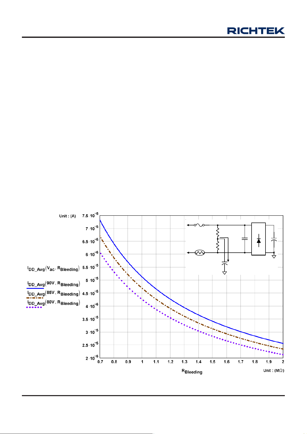
To minimize power loss, it's recommended that the start-
up current is from bleeding resistor. It's not only good for
power saving but also could reset latch mode protection
quickly. Figure 3 shows I
DD_Avg
vs. R
Bleeding
can apply this curve to design the adequate bleeding
resistor.
Gate Driver
A totem pole gate driver is fine tuned to meet both EMI
and efficiency requirement in low power application. An
internal pull low circuit is activated after pretty low VDD to
prevent external MOSFET from accidentally turning on
during UVLO.
Oscillator
To guarantee precise frequency, it's trimmed to 5%
tolerance. It also generates slope compensation saw-tooth,
75% maximum duty cycle pulse and overload protection
slope. It can typically operate at built-in 65kHz center
frequency and features frequency jittering function. Its
curve. User
www.richtek.com
12
Figure 3. I
DD_Avg
vs. R
Bleeding
Curve
R7732-00 May 2011
Page 13
jittering depth is 6% with about 4ms envelope frequency
+
-
+
-
I
BIAS
PRO
V
L_TH
V
H_TH
Deglitch
30µs
Auto
Recovery
V
L_TH
V
H_TH
V
PRO
Auto Recovery / Latch
Normal Operating
Deglitch
50µs
Latch
Auto Recovery / Latch
VDD
VDD OVP : VDD > VR + VZ + 3.8V
(Option)
PRO
PRO
NTC
(Option)
at 65kHz.
Tight Current Limit Tolerance
Since R7732 is the successor of R7731A, its current limit
setting is completely the same as R7731A. Generally,
the saw current limit applied to low cost flyback controller
because of simple design. However, saw current limit is
hard to test in mass production. Therefore, it's generally
"guaranteed by design". The variation of process and
package will make its tolerance wider. It will lead to 20%
to 30% variation when doing OLP test at certain line
voltage. This will cause yield loss in power supply mass
production. Through well foundry control, design and test
/ trim mode in final test, R7732 current limit tolerance is
tight enough to make design easier.
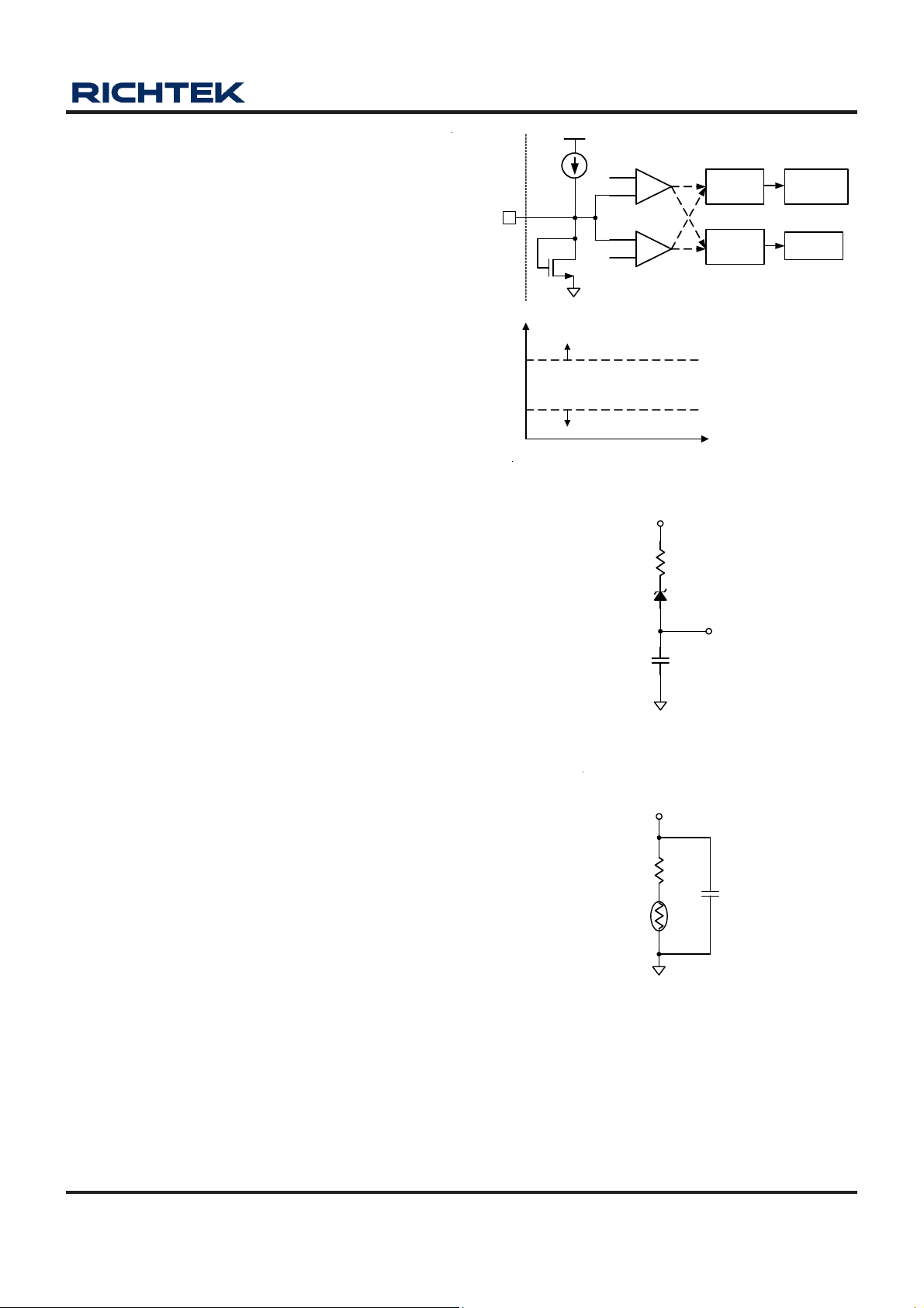
PRO Pin Application
R7732
Figure 4. PRO Pin Diagram
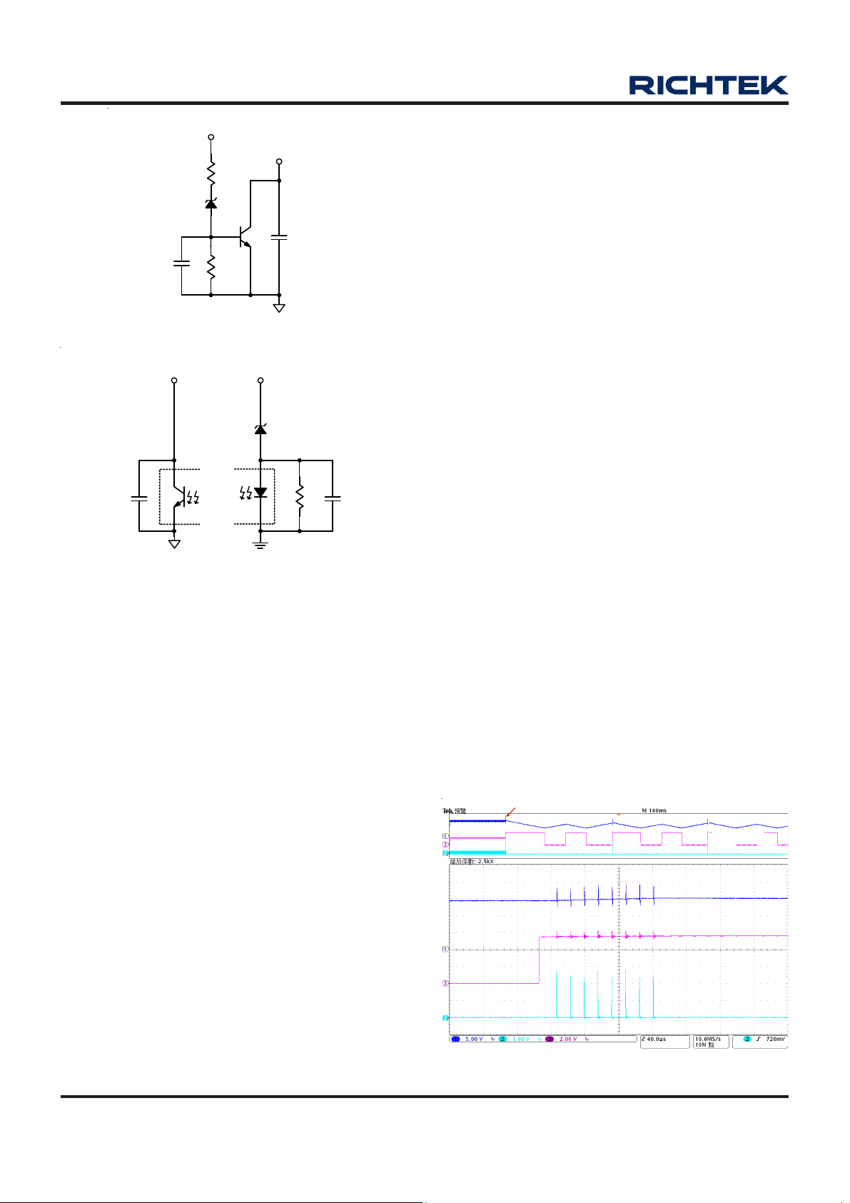
R7732 features a PRO pin, as shown in Figure 4, and it
can be applied for external arbitrary OVP or OTP (ex:
Figure 5 to Figure 8).
If the voltage of PRO pin is greater than pull-low threshold
V
, the controller is enabled and switching will occur.
L_TH
If the voltage of PRO pin falls below pull-low threshold or
rises to pull-high threshold V
, the controller will be
H_TH
shut down and cease to switch after deglitch delay.
PRO pin is built in 1.5V internally, so leave PRO pin open
if you don't need this function. If designer needs to apply
a bypass capacitor on PRO pin, it should not be more
than 1nF. The internal bias current of PRO pin is
100µA(Typ.). R7732 has internal OVP. For arbitrary OVP
or OTP applications which behave as auto recovery or
latch, it can get these by PRO pin. For PRO pin pulling
high function applications, the voltage of PRO pin must
rise above V
greater than 1.2mA and be limited below 5mA.). When IC
enters latch mode, the IC maximum operating current is
40µA (100°C), and it will be release until V
V
PRO pin is guaranteed that below: If the voltage of PRO
TH_OFF
.
(The supply current of PRO pin must be
H_TH
pin reaches 4.1V or falls below 0.47V, the system will be
protected.
R7732-00 May 2011
is fallen to
DD
Figure 5. For VDD OVP Only
Figure 6. For OTP Only
www.richtek.com
13
Page 14
R7732
Secondary Rectifier Short
V
DD
V
CS
V
COMP
VDD
PRO
(Option)
Vo+PRO
(Option) (Option)
Figure 7. For VDD OVP
hiccup(R7732A: latch), the power loss and thermal
during OLP will be averaged to an acceptable level over
the ON/OFF cycle of the IC. This will last until fault is
removed.
• •
• Brownout Protection: During heavy load, this will
• •
trigger 56ms(R7732A: 28ms; R7732H: 36ms) protection
and shut down the system. If it is in light load condition,
system will be shut down after VDD is running low and
triggers UVLO.
• •
• CS Pin Open Protection: When CS pin is opened,
• •
the system will be shut down after couples of cycle. It
could pass CS pin open test easier.
••
• Over Voltage Protection: Output voltage can be
••
roughly sensed by VDD pin. If the sensed voltage
reaches 27V threshold, system will be shut down and
hiccup after 20µs deglitch delay for R7732G/R/H or latch
after 70µs deglitch delay for R7732L/A. This will last
until fault is removed.
Figure 8. For V
Soft-Start
During initial power on, especially at high line, current
spike is kind of unlimited by current limit. Therefore,
besides cycle-by-cycle current limiting, R7732 still
provides soft start function. It effectively suppresses the
stat-up current spike. The typical soft-start duration is
about 40 clock cycles. This will provide more reliable
operation and possibility to use smaller current rating
power MOSFET.
Protection
R7732 provide fruitful protection functions that intend to
protect system from being damaged. All the protection
functions can be listed as below:
• •
• Cycle-by-Cycle Current Limit: This is a basic but
• •
very useful function and it can be implemented easily
in current mode controller.
• •
• Over Load Protection: Long time cycle-by-cycle
• •
current limit will lead to system thermal stress. To further
protect system, system will be shut down after 56ms
(R7732A: 28ms; R7732H: 36ms).
Through our proprietary prolong turn off period during
OUT
OVP
••
• Feedback Open and Opto-Coupler Short: This will
••
trigger OVP or OLP. It depends on which one occurs
first.
••
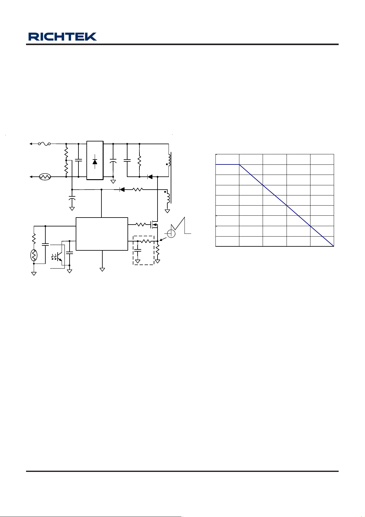
• Secondary Rectifier Short Protection: As shown in
••
Figure 9. The current spike during secondary rectifier
short test is extremely high because of the saturated
main transformer. Meanwhile, the transformer acts like
a leakage inductance. During high line, the current in
power MOSFET is sometimes too high to wait for OLP
delay time. To offer better and easier protection design,
R7732 shut down the controller after couples of cycles
before fuse is blown up.
R7732G
Figure 9. Secondary Rectifier Short Protection
www.richtek.com
14
R7732-00 May 2011
Page 15
R7732
AC Mains
(90V to 265V)
PRO
COMP
GND
GATE
CS
R7732
VDD
5
6
2
1
4
3
NTC
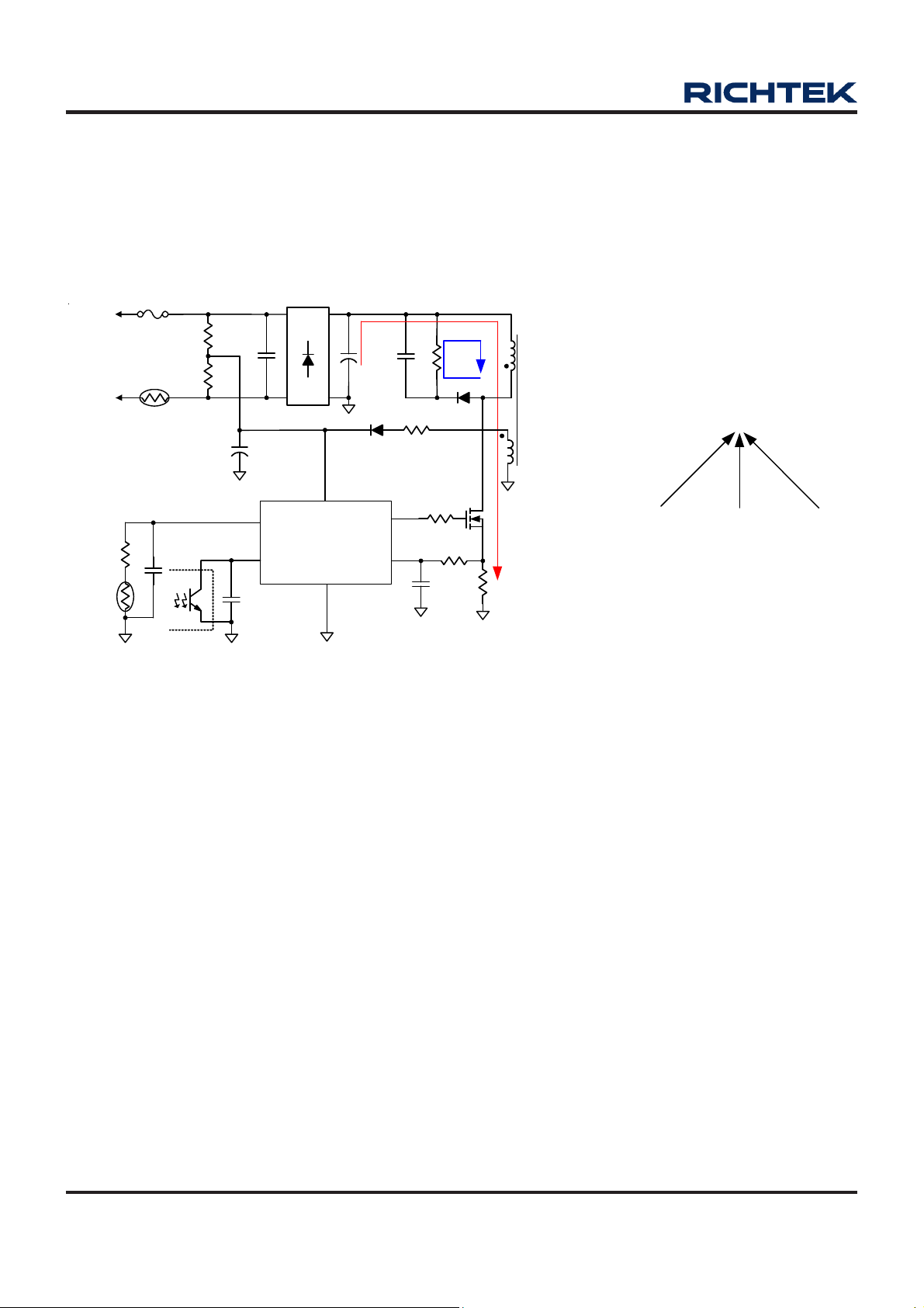
R-C Filter
0.00
0.05
0.10
0.15
0.20
0.25
0.30
0.35
0.40
0.45
0 25 50 75 100 125
Ambient Temperature
Maximum Power Dissipation (W).
Negative Voltage Spike on Each Pin
Negative voltage (< -0.3V) on each pin will cause substrate
injection. It leads to controller damage or circuit false
trigger. Generally, it happens at CS pin due to negative
spike because of improper layout or inductive current
sense resistor. Therefore, it is highly recommended to
add a R-C filter to avoid CS pin damage, as shown in
Figure 10. Proper layout and careful circuit design should
be done to guarantee yield rate in mass production.
on a standard JEDEC 51-3 single-layer thermal test board.
The maximum power dissipation at T
= 25°C can be
A
calculated by the following formula :
P
= (125°C - 25°C) / (250°C/W) = 0.4W for SOT-23-
D(MAX)
6 package
The maximum power dissipation depends on the operating
ambient temperature for fixed T
resistance, θ
. For the R7732 package, the derating curve
JA
J (MAX)
and thermal
in Figure 11 allows the designer to see the effect of rising
ambient temperature on the maximum power dissipation.
Figure 10. R-C Filter on CS Pin
Thermal Considerations
For continuous operation, do not exceed absolute
maximum junction temperature. The maximum power
dissipation depends on the thermal resistance of the IC
package, PCB layout, rate of surrounding airflow, and
difference between junction and ambient temperature. The
maximum power dissipation can be calculated by the
following formula :
P
Where T
the ambient temperature, and θ
thermal resistance.
For recommended operating condition specifications of
the R7732, the maximum junction temperature is 125°C
and TA is the ambient temperature. The junction to ambient
thermal resistance, θ
23-6 packages, the thermal resistance, θJA, is 250°C/W
R7732-00 May 2011
= (T
D(MAX)
J(MAX)
- T
J(MAX)
A
) / θ
JA
is the maximum junction temperature, TA is
is the junction to ambient
JA
, is layout dependent. For SOT-
JA
Figure 11. Derating Curves for R7732 Package
Layout Considerations
A proper PCB layout can abate unknown noise interference
and EMI issue in the switching power supply. Please refer
to the guidelines when you want to design PCB layout for
switching power supply:
} The current path (1) from bulk capacitor, transformer,
MOSFET, Rcs return to bulk capacitor is a huge high
frequency current loop. It must be as short as possible
to decrease noise coupling and kept a space to other
low voltage traces, such as IC control circuit paths,
especially.
} The path (2) from RCD snubber circuit to MOSFET is
also a high switching loop, too. Keep it as small as
possible.
} It is good for reducing noise, output ripple and EMI issue
to separate ground traces of bulk capacitor (a), MOSFET
(b), auxiliary winding (c) and IC control circuit (d). Finally,
connect them together on bulk capacitor ground (a).
www.richtek.com
15
Page 16
R7732
(a)
(d)
(b)
(1)
(c)
(2)
Auxiliary
Ground (c)
IC
Ground (d)
Trace Trace
Trace
MOSFET
Ground (b)
C
BULK
Ground (a)
AC Mains
(90V to 265V)
PRO
COMP
GND
GATE
CS
R7732
VDD
5
6
2
1
4
3
NTC
C
BULK
The areas of these ground traces should be kept large.
} Placing bypass capacitor for abating noise on IC is
highly recommended. The bypass capacitor should be
placed as close to controller as possible.
} In order to minimize reflected trace inductance and EMI,
it is minimized the area of the loop connecting the
secondary winding, the output diode, and the output
filter capacitor. In addition, apply sufficient copper area
at the anode and cathode terminal of the diode for
heatsinking. Apply a larger area at the quiet cathode
terminal. A large anode area can increase high-frequency
radiated EMI.
Figure 12. PCB Layout Guide
www.richtek.com
16
R7732-00 May 2011
Page 17
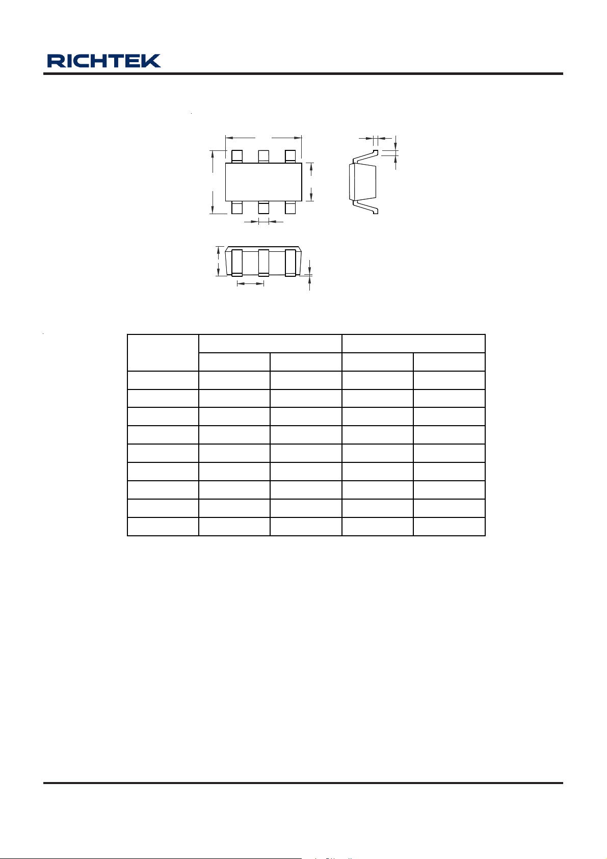
Outline Dimension
A
A1
e
b
B
D
C
H
L
Dimensions In Millimeters
Dimensions In Inches
Symbol
Min Max Min Max
A 0.889 1.295 0.031 0.051
A1 0.000 0.152 0.000 0.006
B 1.397 1.803 0.055 0.071
b 0.250 0.560 0.010 0.022
C 2.591 2.997 0.102 0.118
D 2.692 3.099 0.106 0.122
e 0.838 1.041 0.033 0.041
H 0.080 0.254 0.003 0.010
L 0.300 0.610 0.012 0.024
R7732
SOT-23-6 Surface Mount Package
Richtek Technology Corporation
Headquarter
5F, No. 20, Taiyuen Street, Chupei City
Hsinchu, Taiwan, R.O.C.
Tel: (8863)5526789 Fax: (8863)5526611
Richtek Technology Corporation
Taipei Office (Marketing)
5F, No. 95, Minchiuan Road, Hsintien City
Taipei County, Taiwan, R.O.C.
Tel: (8862)86672399 Fax: (8862)86672377
Email: [email protected]
Information that is provided by Richtek Technology Corporation is believed to be accurate and reliable. Richtek reserves the right to make any change in circuit design,
specification or other related things if necessary without notice at any time. No third party intellectual property infringement of the applications should be guaranteed
by users when integrating Richtek products into any application. No legal responsibility for any said applications is assumed by Richtek.
R7732-00 May 2011
www.richtek.com
17
Page 18

 Loading...