

Page 1
New Electro-Optical Design
13mm (1/2 Inch) Diameter, 9-stage, Side-on Type
Our new electro-optic construction allows Hamamatsu to introduce
an improved line of compact side-on PMTs. The X-axis anode uniformity full width half maximum (FWHM) is greater than existing
models. This wider "sweet" spot increases detection efficiency and
can make optical alignment easier.
The R6357 is a unique addition, it is the new meshless multialkali
compact PMT having over 100mA/W photocathode radiant sensitivity.
NEW COMPACT TYPE
PMT SERIES
APPLICATIONS
Emission Spectroscopy (ICP, Direct Reader)
Environmental Monitoring (NOx, SO2, etc.)
Fluorescence Immunoassay
Chemiluminescence Immunoassay
Hygiene Monitor (Bio Luminescence)
X-ray Phototimer
Fluorometer
Microscope (Laser Scanning Microscope)
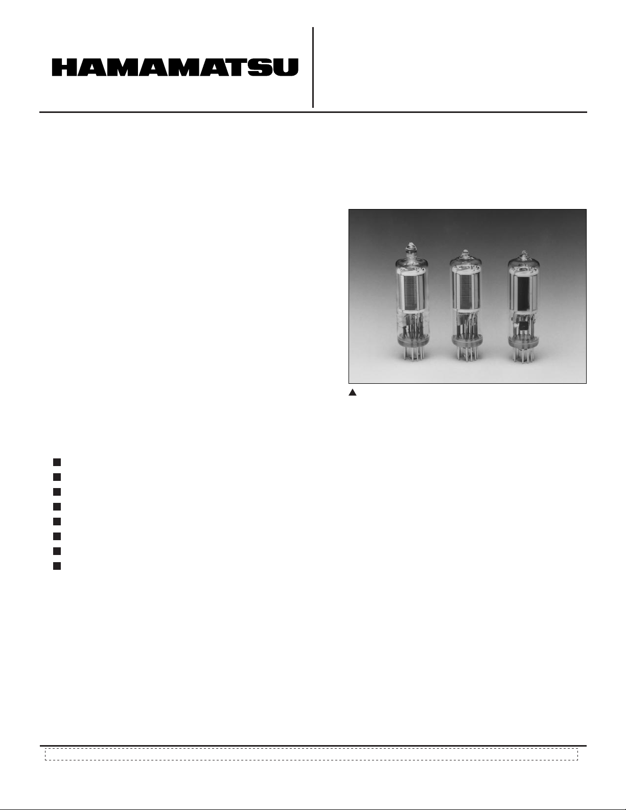
Left: Quartz window Center: UV window
Right: Meshless type (R6357)
Subject to local technical requirements and regulat ions, availability of products included in this promotional material may va r y. Please consult with our sales office.
Information furnished by HAMA M ATSU is believed to be reliable. However, n o responsibility is assumed for possible inaccuracies or omissions. Specifications are
subject to change without notice. No patent rights are granted to any of the circuits described herein.
1998 Hamamatsu Photonics K.K.
©
Page 2
NEW COMPACT TYPE PMT SERIES
Side-On New Compact Type Photomultiplier Tubes
Spectral Response
Peak
Photo-
Type No.
R6350
R6351
Remarks
For UV to visible range,
general purpose.
Synthetic silica
window type of R6350
Range
Wavelength
(nm) (nm) (Vdc)
185 to 650
160 to 650
340
340
cathode
Material
Sb-Cs
Sb-Cs
Window
Material
U
Q
Outline
No.
1
2
Dynode
Structure
No. of
Stages
CC/9
CC/9
Socket
Socket
Assembly
E678-11U/
E678-11U/
Maximum
Ratings
Anode to
Cathode
Voltage
1250
1250
Cathode Sensitivity
Luminous
Average
Anode
Min.
Current
(mA)
(µA/lm)
0.01
0.01
20
20
Typ.
(µA/lm)
40
40
R6352
R6353
R6354
R6355
R6356
R6357 *
R6358
* Achieved the higher photocathode sensitivity by eliminating the mesh in front of the photocathode.
It also features no output variation, disturbed by the mesh, when the incident light spot to the photocathode is small.
NOTE Photocathode materials
High sensitivity
variant of R6350
Low dark current
bialkali photocathode
For UV range
For UV to near IR range,
general purpose
High sensitivity
variant of R6355
High sensitivity
variant of R6356,
Meshless type
Low dark current
variant of R6356
BA: Bialkali
LBA: Low dark current bialkali
MA: Multialkali
LMA: Low dark current multialkali
Dynode structure
CC: Circular-cage
Averaged over any interval of 30 seconds maximum.
185 to 750
185 to 680
160 to 320
185 to 850
185 to 900
185 to 900
185 to 830
420
400
230
530
600
450
530
BA
LBA
Cs-Te
MA
MA
MA
LMA
Window materials
Q: Synthetic silica
U: UV glass
See optional accessories
U
U
Q
U
U
U
U
1
CC/9
1
CC/9
2
CC/9
1
CC/9
1
CC/9
1
CC/9
1
CC/9
E678-11U/
E678-11U/
E678-11U/
E678-11U/
E678-11U/
E678-11U/
E678-11U/
Outline No.
See Fig. 9
The maximum ambient temperature
range is -80 to +50°C.
1250
1250
1250
1250
1250
1250
1250
0.01
0.01
0.01
0.01
0.01
0.01
0.01
80
30
—
80
140
350
140
120
70
—
150
250
500
200
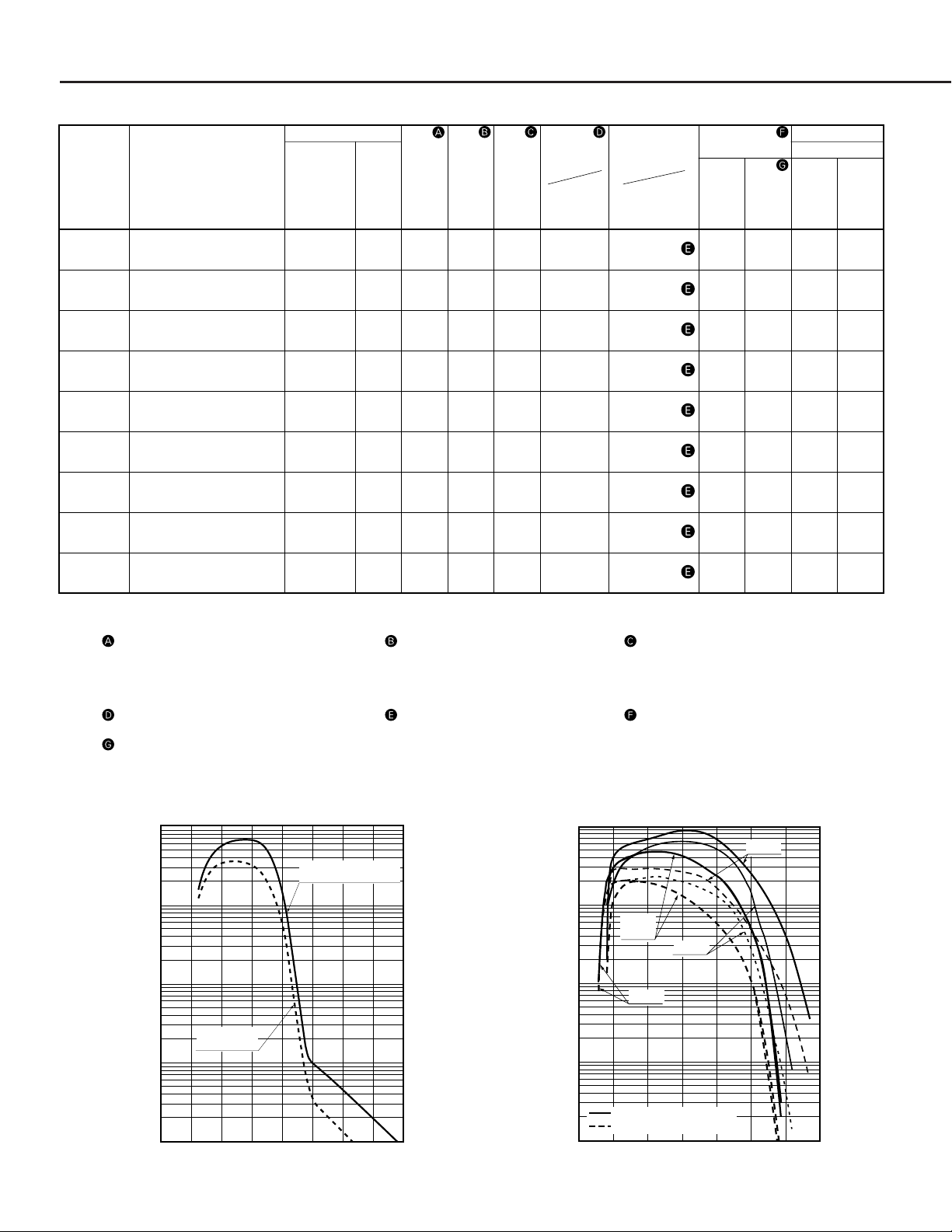
Figure 1: Typical Spectral Response of Cs-Te
TPMSB0128EA
100
CATHODE RADIANT
SENSITIVITY
10
1
QUANTUM
QUANTUM EFFICIENCY (%)
0.1
CATHODE RADIANT SENSITIVITY (mA/W)
0.01
EFFICIENCY
100 300200 400 500
WAVELENGTH (nm)
Figure 2: Typical Spectral Response of BA, LBA, Sb-Cs
TPMSB0114EA
100
R6352
10
1
QUANTUM EFFICIENCY (%)
0.1
CATHODE RADIANT SENSITIVITY (mA/W)
0.01
100
R6350,
R6351
R6353
R6351
RADIANT SENSITIVITY
QUANTUM EFFICIENCY
200 400 600
WAVELENGTH (nm)
700500300
800
Page 3
Cathode Sensitivity
Blue
Red/
(5-58)
Typ.
(µA/lm-b)
5
Radiant
White
Ratio
Typ.
(mA/W) (Vdc) (A/lm)
—
Typ.
48
Anode to
Cathode
Supply
Voltage
1000
Anode Sensitivity
Luminous
Min.
Typ.
(A/lm)
50
300
3.6 × 10
Anode Characteristics
Current
5
Amplifi-
cation
Typ.
7.5 × 10
6
Radiant
Typ.
(nm)
Anode Dark
Current
(After 30 min.)
Max.
Typ.
(nA)
0.5
5
Time Response
Electron
Rise
Transit
Time
Time
Typ.
1.4
Typ.
(ns)(nA)
15
(ns)
Photon counting type:
R6350P: 10cps Typ.
Type No.Notes
R6350
6 × 10
5
5
5
5
5
5
5
5
5
—
48
10
—
90
6.5
7.5
—
65
—
—
62
6
0.15
7
0.3
13
0.4
0.15
Measured using red filter Toshiba R-68.
Anode characteristics are measured with the supply voltage
and voltage distribution ratio specified by Note .
Voltage distribution ratio and voltage.
45
60
105
70
Electrodes
1000
1000
1000
1000
1000
1000
1000
1000
50
100
100
—
100
400
1000
300
K Dy11Dy21Dy31Dy41Dy51Dy61Dy71Dy81Dy9 P
300
700
400
—
600
2500
2000
700
3.6 × 10
5.2 × 10
3.7 × 10
1.8 × 10
1.8 × 10
4.2 × 10
2.5 × 10
Distribution Ratio
Supply Voltage: 1000Vdc, K: Cathode, Dy: Dynode, P: Anode
7.5 × 10
5.8 × 10
5.7 × 10
3.5 × 10
6
0.5
6
6
0.1
6
3 × 10
4 × 10
1 × 10
4 × 10
Measured at the peak wavelength.
: at 254nm
0.5
6
7
6
6
0.1
5
1.4
1
10
1.4
2
1.4
5
1.4
1
10
1.4
1
10
1.4
2
10
1.4
1
1.4
11
15
15
Photon counting type:
15
R6353P: 10cps Typ.
15
15
15
15
Photon counting type:
15
R6358P: 20cps Typ.
Refer to Note .
R6351
R6352
R6353
R6354
R6355
R6356
R6357 *
R6358
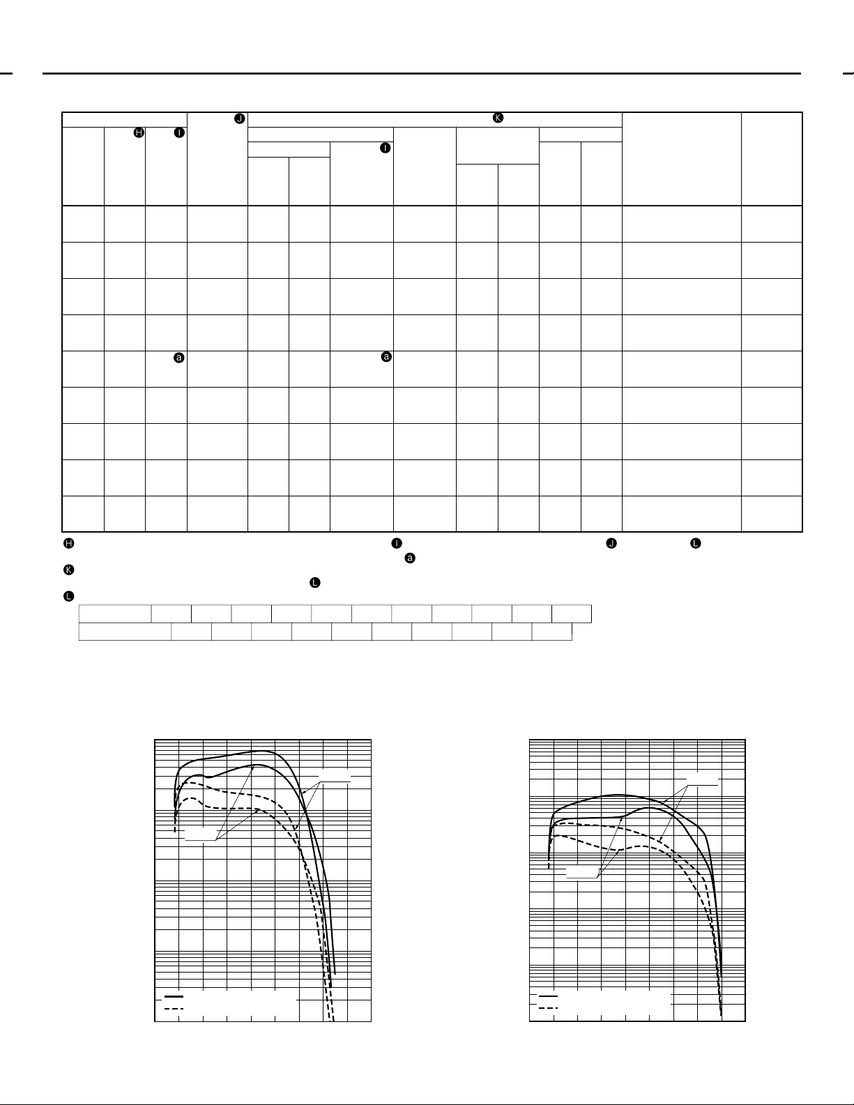
Figure 3: Typical Spectral Response of MA, LMA
TPMSB0115EA
100
R6358
10
R6355
1
QUANTUM EFFICIENCY (%)
0.1
CATHODE RADIANT SENSITIVITY (mA/W)
RADIANT SENSITIVITY
0.01
QUANTUM EFFICIENCY
100
200 400 600
WAVELENGTH (nm)
700500300
800
900 1000
Figure 4: Typical Spectral Response of High Sensitivity MA
TPMSB0116EA
1000
R6357
100
10
R6356
1
QUANTUM EFFICIENCY (%)
0.1
CATHODE RADIANT SENSITIVITY (mA/W)
RADIANT SENSITIVITY
0.01
QUANTUM EFFICIENCY
100
200 400 600 800 900 1000
WAVELENGTH (nm)
700500300
Page 4
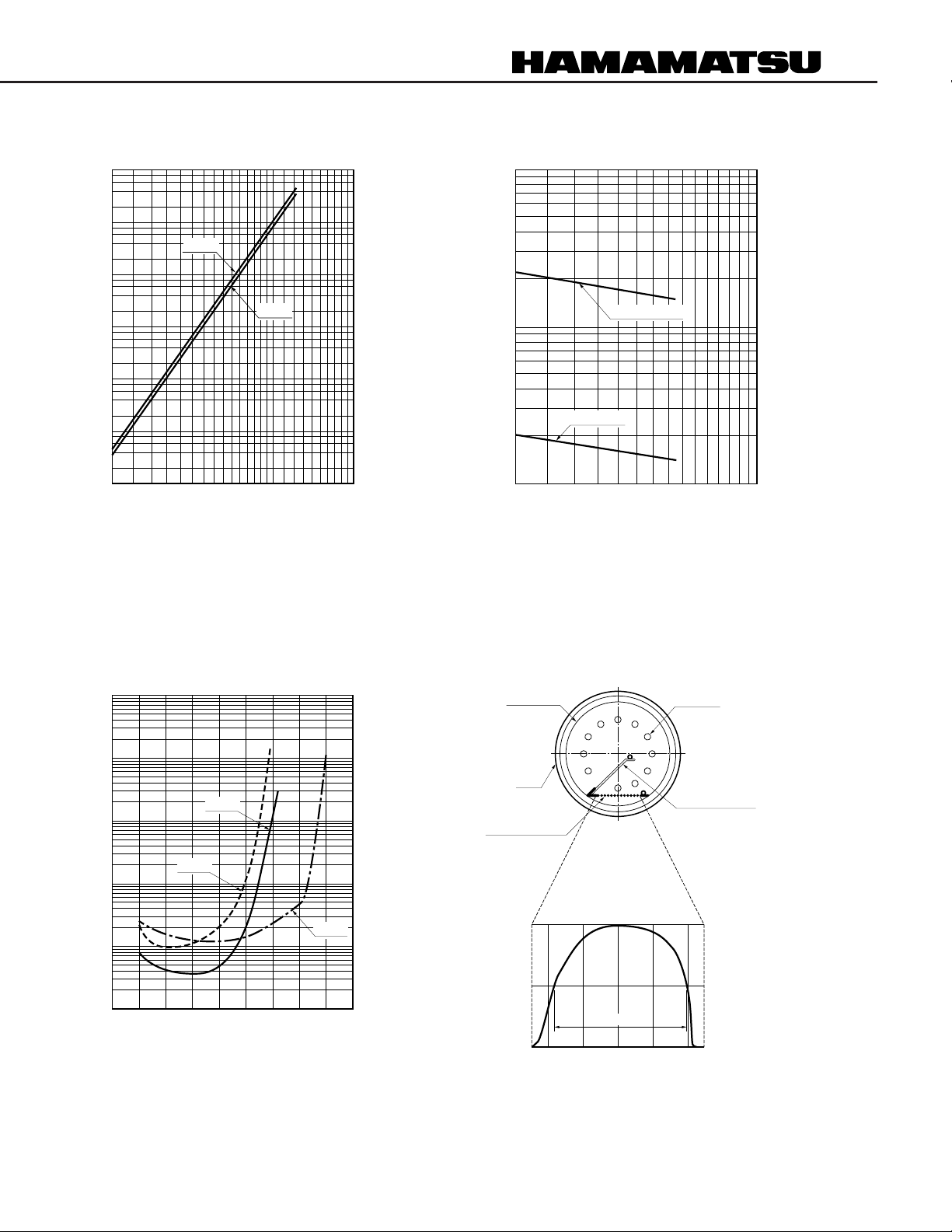
Figure 5: Typical Current Amplification
Figure 6: Typical T ime Response
TPMSB0117EA
8
10
7
10
R6356
6
10
5
10
GAIN
4
10
3
10
2
10
250 300 15001000
SUPPLY VOLTAGE (V)
TPMSB0118EA
100
R6350
TRANSIT TIME
10
TIME (ns)
RISE TIME
700500
2000
1
500
SUPPLY VOLTAGE (V)
15001000
2000
Figure 7: Typical ENI Characteristics
TPMSB0119EA
-12
10
-13
10
R6353
-14
10
R6350
-15
10
EQUIVALENT NOISE INPUT (W)
-16
10
-17
10
100
200 300 400 600 700 900
WAVELENGTH (nm)
Figure 8: Typical Anode Uniformity
INSULATOR
BULB
MESH
R6357: MESHLESS
TYPE
R6357
800500
1000
100
50
3.7mm
0
ANODE RELATIVE OUTPUT (%)
LEFT RIGHT
1221
0
BASE PIN
TOP VIEW
PHOTOCATHODE
(mm)
TPMSC0036EA
Page 5
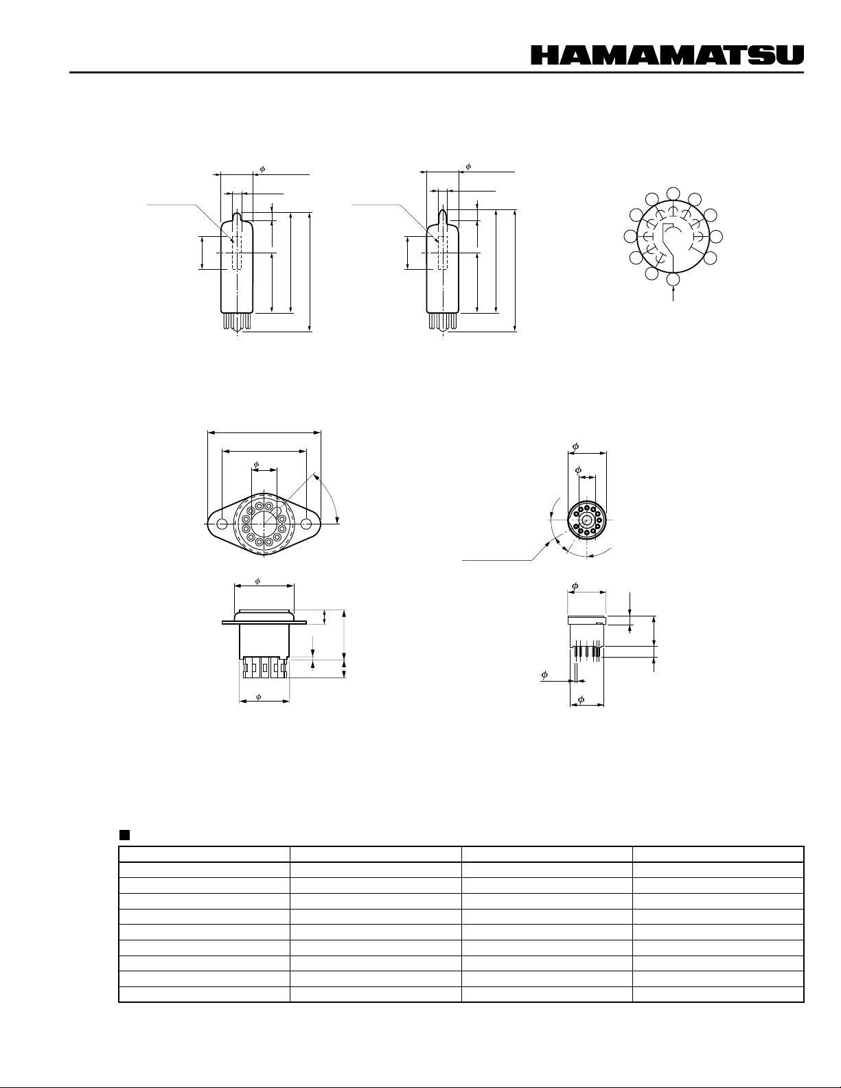
Figure 9: Dimensional Outline and Basing Diagram (Unit: mm)
Outline No.1 Outline No.2
13.5 ± 0.8
4MIN.
7 ± 2
24.0 ± 1.5
PHOTO-
CATHODE
13MIN.
UV WINDOW
13.5 ± 0.8
4MIN.
3 ± 2
40 ± 2
24.0 ± 1.5
50MAX.
PHOTO-
CATHODE
13MIN.
QUARTZ WINDOW
Socket
E678-11U
24
18
5.5
For direct soldering to PC board
42 ± 2
52MAX.
E678-11T (Option):
12.4
5.5
DY6
DY5
DY4
4
DY3
DY2
DY1
DIRECTION OF LIGHT
7
6
5
3
2
1
BOTTOM VIEW
DY7
8
DY8
9
10
DY9
11
P
K
TPMSA0034EB
30
0.5
°
30°
12.4
2.7
10.5
3
11
TACCA0161EA
13
11
0.5
45°
DIRECTION
OF LIGHT
3
10.5
4
TACCA0181EA
Remaining Hamamatsu Photonics 1/2" side on PMT anode cap types and compact types will be discontinued by the
year 2000.
We recommend the new compact types instead of those current in use.
Correlation among anode cap type, current compact type and new compact type
TYPE/GRADE
Sb-Cs/UV
Sb-Cs/Q
BA/UV HIGH
LBA/UV
MA/UV
MA/UV HIGH
MA/UV HIGH
LMA/UV
Cs-Te/Q
NOTE UV: UV WINDOW, Q: QUARTZ WINDOW, HIGH: HIGH SENSITIVITY
ANODE CAP TYPE CURRENT COMPACT TYPE NEW COMPACT TYPE
R300/R444
R306
—
—
R889
—
—
—
R427
R1414/R1413
R1656
R5785
R2371
R1547/R1546
R3823
R3823-03
R4457
R1657
R6350
R6351
R6352
R6353
R6355
R6356
R6357
R6358
R6354
Page 6
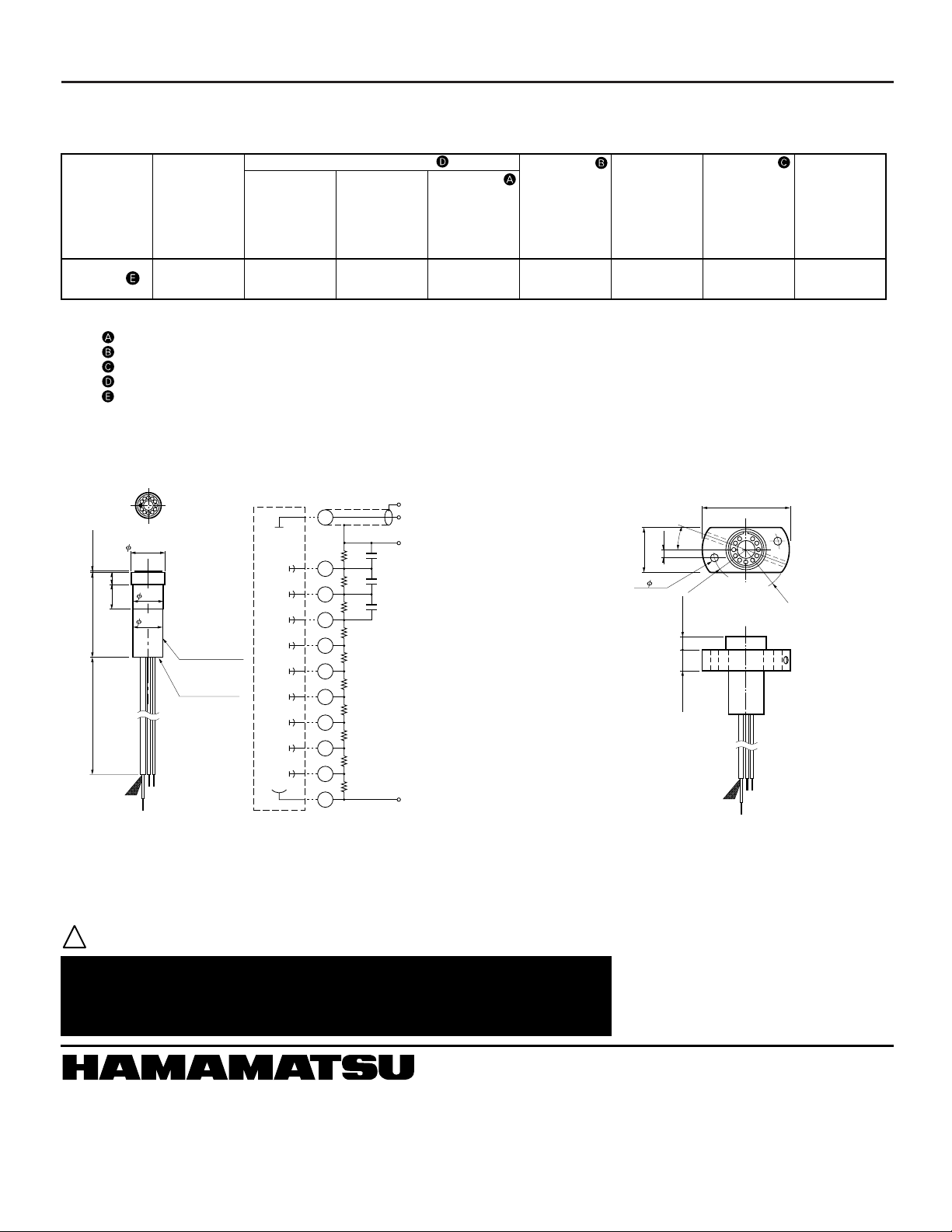
NEW COMPACT TYPE PMT SERIES
Optional Accessories
D-Type Socket Assembly
Maximum Ratings
Type No.
Ground
Potential
Electrode
Supply
Voltage
between
Case and
Pins
(Vdc)
Supply
Voltage
between
Power Supply
Terminals
(Vdc)
Voltage
Divider
Current
(mA)
E850-13 Anode 12501500 5 × 10
E850-22: with SHV, BNC connector
NOTE Measured with the maximum supply voltage.
Measured with a supply voltage of 1000V.
The current at witch the output linearity is kept within ±5%.
Operating temperature range -20 to +50°C.
Supplied with a separate mounting flange. See below for assembled dimensions.
Dimensional Outline and Circuit Diagram (Unit: mm)
E850-13
PMT
0.5MAX.
5
10
35.0 ± 0.5
450 ± 10
14.0 ± 0.3
12.6
12.4
HOUSING
(INSULATOR)
POTTING
COMPOUND
P
DY9
DY8
DY7
DY6
DY5
DY4
DY3
DY2
DY1
K
SOCKET PIN No.
11
R10
10
R9
9
R8
8
R7
7
R6
6
R5
5
R4
4
R3
3
R2
2
R1
1
SIGNAL GND
SIGNAL OUTPUT RG-174/U
(BLACK)
POWER SUPPLY GND
AWG 22 (BLACK)
C3
C2
C1
R1 to R10
C1 to C3
-HV
AWG 22 (VIOLET)
: 330kΩ
: 0.01µF
Leakage
Current
in Signal
TACCA0096EA TACCA0097EB
Max.
(A)
Total
Voltage
Divider
Maximum
Linear
Output
Resistance
DC Mode
(MΩ)
-10
3.3 15 (at 1000V) DC/Pulse0.38
Mounting Flange for E850-13
36.0 ± 0.3
20°
2.5
15.0 ± 0.3
2- 3.2
R11
5.0 ± 0.5
7.0 ± 0.3
in
(µA)
Signal
Output
R15
!
WARNING ~High Voltage~
The product is operated at high voltage potential. Further, the metal housing of the product is
connected to the photocathode (potential) so that it becomes a high voltage potential when the
product is operated at a negative high voltage (anode grounded).
Accordingly, extreme safety care must be taken for the electrical shock hazard to the operator or
the damage to the other instruments.
HAMAMATSU PHOTONICS K.K., Electron Tube Center
314-5, Shimokanzo, Toyooka-village, Iwata-gun, Shizuoka-ken, 438-0193, Japan, Telephone: (81)539/62-5248, Fax: (81)539/62-2205
U.S.A.:
Hamamatsu Corporation: 360 Foothill Road, P. O. Box 6910, Bridgewater. N.J. 08807-0910, U.S.A., Telephone: (1)908-231-0960, Fax: (1)908-231-1218
Germany:
Hamamatsu Photonics Deutschland GmbH: Arzbergerstr. 10, D-82211 Herrsching am Ammersee, Germany, Telephone: (49)8152-375-0, Fax: (49)8152-2658
France:
Hamamatsu Photonics France S.A.R.L.: 8, Rue du Saule Trapu, Parc du Moulin de Massy, 91882 Massy Cedex, France, Telephone: (33)1 69 53 71 00, Fax: (33)1 69 53 71 10
United Kingdom:
North Europe:
Italy:
Hamamatsu Photonics UK Limited: Lough Point, 2 Gladbeck Way, Windmill Hill, Enfield, Middlesex EN2 7JA, United Kingdom, Telephone: (44)181-367-3560, Fax: (44)181-367-6384
Hamamatsu Photonics Norden AB: Färögatan 7, S-164-40 Kista Sweden, Telephone: (46)8-703-29-50, Fax: (46)8-750-58-95
Hamamatsu Photonics Italia: S.R.L.: Strada della Moia, 1/E, 20020 Arese, (Milano), Italy, Telephone: (39)02-935 81 733, Fax: (39)02-935 81 741
TPMS1032E03
OCT. 1998 IP
Printed in Japan (1000)
 Loading...