

Page 1
R5011ANX
z
z
z
z
z
z
z
Transistors
10V Drive Nch MOSFET
R501 1ANX
Structure
Silicon N-channel MOSFET
Features
1) Low on-resistance.
2) Fast switching speed.
3) Gate-source voltage (V
GSS)
guaranteed to be r30V.
4) Drive circuits can be simple.
5) Parallel use is easy.
Applications
Switching
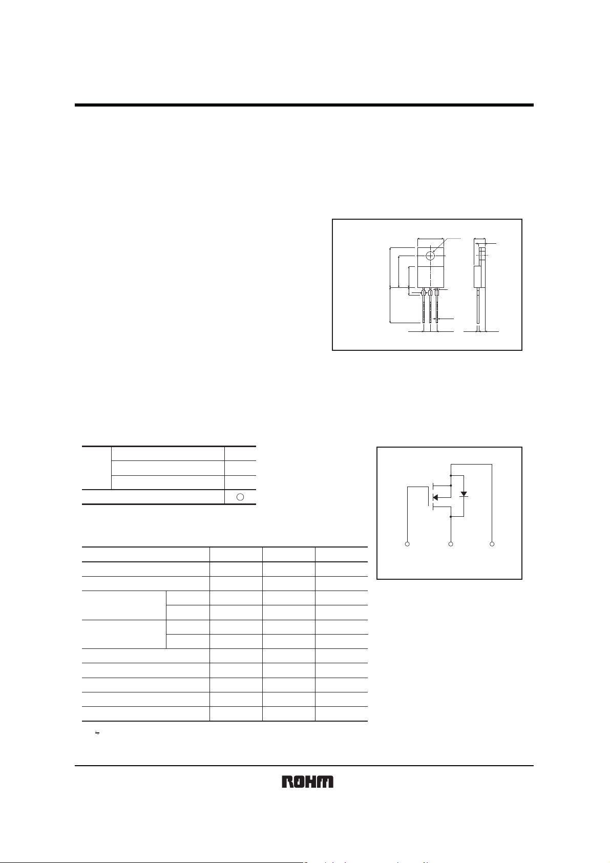
Dimensions (Unit : mm)
TO-220FM
15.0
12.0
8.02.5
14.0
(1)Base
(2)Collector
(3)Emitter
φ3.2
10.0
1.3
1.2
0.8
2.54 2.62.54
(2)(3)(1)
4.5
2.8
0.75
Packaging specifications
z
Package
Code
Type
Basic ordering unit (pieces)
R5011ANX
z
Absolute maximum ratings (Ta=25qC)
Parameter
Drain-source voltage
Gate-source voltage
Drain current
Source current
(Body Diode)
Continuous
Pulsed
Continuous
Pulsed
Avalanche Current
Avalanche Energy
Total power dissipation (Tc=25°C)
Channel temperature
Range of storage temperature
∗1 Pw≤10μs, Duty cycle≤1%
∗2 L 500μH, V
∗3 Limited only by maximum tempterature allowed
DD
=50V, RG=25Ω, Starting, Tch=25°C
Bulk
−
500
∗3
∗1
∗3
∗1
∗2
∗2
−55 to +150
Limits
500
±30
±11
±44
11
44
5.5
8.1
50
150
Symbol
V
DSS
V
GSS
I
D
I
DP
I
S
SP
I
AS
I
E
AS
P
D
Tch
Tstg °C
Inner circuit
Unit
V
V
A
A
A
A
A
mJ
W
°C
(1) (2) (3)
(1) Gate
(2) Drain
(3) Source
∗1
∗1 Body Diode
1/5
Page 2
Transistors
z
z
z
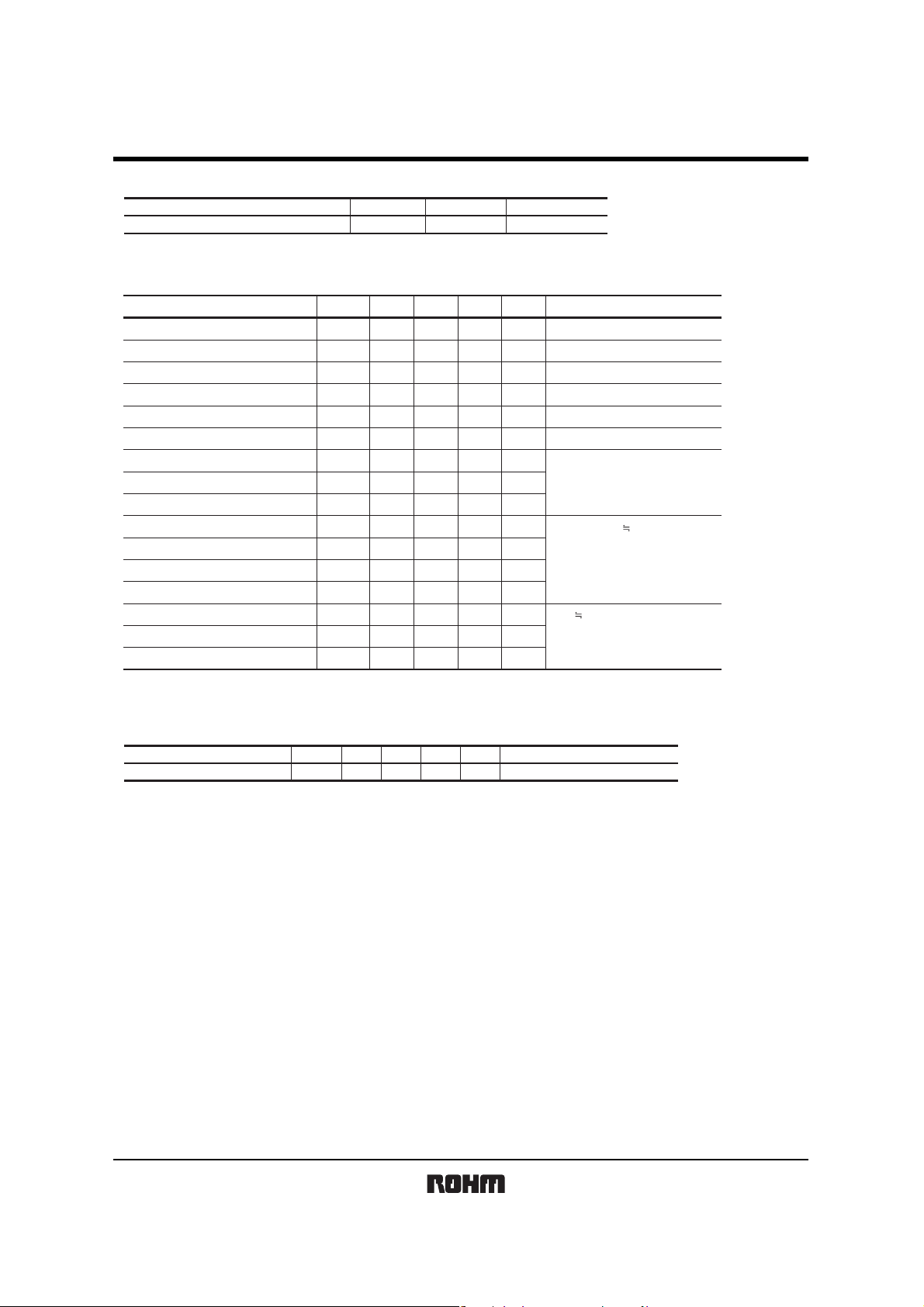
Thermal resistance
Parameter
Channel to case
z
Electrical characteristics (Ta=25qC)
Parameter
Gate-source leakage
Drain-source breakdown voltage
Zero gate voltage drain current
Gate threshold voltage
Static drain-source on-state resistance
Forward transfer admittance
Input capacitance
Output capacitance
Reverse transfer capacitance
Turn-on delay time
Rise time
Turn-off delay time
Fall time
Total gate charge
Gate-source charge
Gate-drain charge
∗ Pulsed
z
Body diode characteristics (Source-drain) (Ta=25qC)
Parameter Symbol
V
SD
∗ Pulsed
Symbol Limits Unit
Rth(ch-c)
Symbol
I
V
(BR)DSS
I
V
R
| Y
C
C
t
t
Q
GSS
DSS
GS(th)
DS(on)
fs
C
iss
oss
rss
d(on)
t
r
d(off)
f
t
g
Q
Q
gs
gd
Min.
−
500
−
2.5
∗
−
∗
|
3.5
−
−
−
∗
−
∗
−
∗
−
∗
−
∗
−
∗
−
∗
−
Min. Typ. Max.
∗
−−1.5 V IS= 11A, VGS=0VForward voltage
2.5
Max. Unit Conditions
Typ.
±100
−
−
−
100
−
4.5
−
0.5
0.38
−
−
1000
400
−
−
−
35
− ns
26
− VGS=10Vns
28
− RL=45.5Ωns
75
− RG=10Ωns
30
− VDD250V
30
− nC
7
− nC
12
Unit
°C/W
nA V
V
μA
V
Ω
S
pF
pF
pF
nC
GS
D
=1mA, VGS=0V
I
DS
V
V
DS
D
=5.5A, VGS=10V
I
I
D
=5.5A, VDS=10V
V
DS
V
GS
f=1MHz
I
D
=5.5A, VDD 250V
I
D
=11A
V
GS
R
L
=22.7Ω / RG=10Ω
Conditions
R5011ANX
=±30V, VDS=0V
=500V, VGS=0V
=10V, ID=1mA
=25V
=0V
=10V
2/5
Page 3
Transistors
z
ge
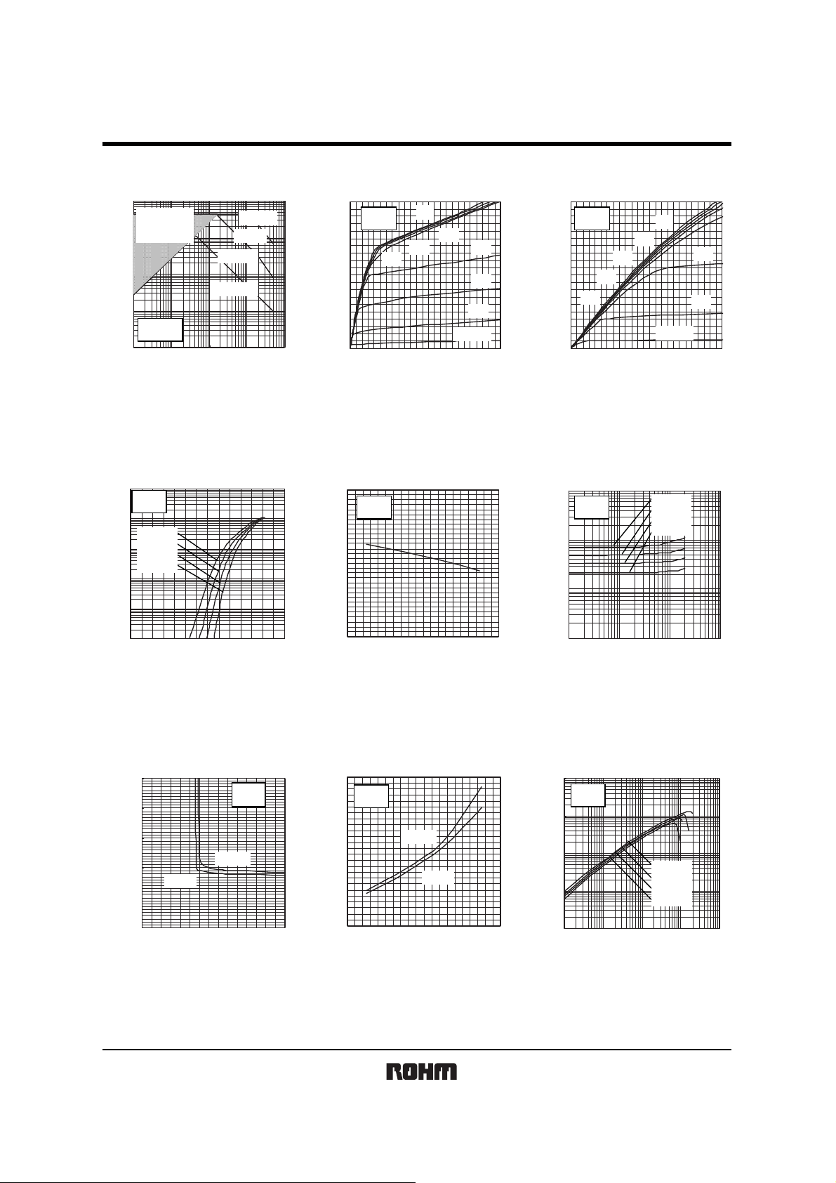
Electrical characteristic curves
100
Oper ation in thi s
area i s li mi ted
by R
DS(ON)
10
(A)
D
1
0.1
DRAIN CURRENT : I
Ta = 25°C
Sing le Pulse
0.01
0.1 1 10 100 1000
DRAIN -SOUR CE VOLTAGE : VDS ( V )
Fi g.1 M aximum Safe O perating Aera
100
VDS= 10V
Pulsed
10
(A)
Ta= 125°C
D
Ta= 75°C
1
Ta= 25°C
Ta= -25°C
0.1
DRAIN CURRENT : I
0.01
0.001
0.0 1.5 3.0 4.5 6. 0
GATE- SOURC E VOLTAGE : VGS (V)
Fi g.4 T ypical Transf er Char acteri stic s
PW=100us
PW=1ms
PW=100ms
DC operati on
20
Ta= 25°C
Pulsed
15
(A)
D
10
5
DRAIN CURRENT: I
0
0 10203040 50
DRAIN-SOURCE VOLTAGE: VDS (V)
Fig .2: Typical Output Character istic s(㸇)
6
VDS= 10V
(V)
I
= 1mA
D
5
GS(th)
4
3
2
1
GATE TH RESHOLD VOLTAGE: V
0
-50 0 50 100 150
CHANNEL TEMPERATURE: Tch (°C)
Fi g.5 Gate T hreshol d Voltag e
vs. Channel Temperatur e
10V
8.0V
6.5V
VGS= 4. 5V
6.0V7.0V
5.5V
5.0V
R5011ANX
10
Ta= 25°C
Pulsed
8
(A)
D
6
6.5V
4
6.0V
DRAIN CURRENT: I
2
0
012345
DRAIN-SOURCE VOLTAGE: VDS (V)
Fi g.3: T ypic al Output C haracter ist ics(㸈)
10
VGS= 10V
Pulsed
(ȍ)
1
DS(on)
0.1
RESIST ANCE : R
STATIC DRAIN-SOURCE ON-STATE
0.01
0.1 1 10 100
DRAIN CURRENT : ID (A)
Fi g.6 St atic D rain- Sourc e On-State
Resi stance vs. D rain C urr ent
7.0V
8.0V
10V
VGS= 4.5V
Ta= 125°C
Ta= 75°C
Ta= 25°C
Ta= -25°C
5.5V
5.0V
1
0.9
0.8
(ȍ)
0.7
DS(on)
0.6
0.5
0.4
ID= 5.5A
0.3
RESIST ANCE : R
0.2
0.1
STATIC DRAIN-SOURCE ON-STATE
0
0 5 10 15
GATE- SOURC E VOLTAGE : VGS (V)
Fi g.7 Stat ic D rain- Source On-State
Resi stance vs. Gat e Source Vol ta
Ta= 25°C
Pulsed
ID= 11. 0A
1
VGS= 10V
Pulsed
0.8
) (ȍ)
DS(on
0.6
0.4
RESIST ANCE : R
0.2
STAT IC DR AIN-SOU RCE ON -STAT E
0
-50 0 50 100 150
Fi g.8 St atic D rain- Sourc e On-State
R esist ance vs. Channel Temperat ure
ID= 11.0A
ID= 5.5A
CHANNEL TEMPERATURE: Tch (°C)
100
VDS= 10V
Pulsed
10
1
|Yfs| (S)
0.1
FOR WARD TRANSF ER ADM ITTAN CE :
0.01
0.01 0.1 1 10 100
DRAIN CURRENT : ID (A)
Fi g.9 F orward T ransfer Admittanc e
vs. Dr ain Current
Ta= -25°C
Ta= 25°C
Ta= 75°C
Ta= 125°C
3/5
Page 4

Transistors
R5011ANX
100
VGS= 0V
(A)
DR
Pulsed
10
1
0.1
REVERSE DRAIN CURRENT : I
0.01
0 0.5 1 1.5
SOURCE-DRAIN VOLTAGE : VSD (V)
Fi g.10 R evers e Drai n Curr ent vs.
Sours e- Drain Voltag e
1000
(ns)
rr
100
Ta= 25°C
di / dt = 100A / μs
V
= 0V
GS
REVERSE RECOVERY TIME: t
10
0.1 1 10 100
Pulsed
REVERSE DRAIN CURRENT : IDR (A)
Fi g.13 R ever se Reco very Ti me
vs.R everse D rain C urr ent
Ta= 125°C
Ta= 75°C
Ta= 25°C
Ta= -25°C
10000
1000
C
rss
100
Ta= 25°C
10
CAPACITANCE : C (pF)
f= 1MH z
V
= 0V
GS
1
0.1 1 10 100 1000
DRAIN-SOURCE VOLTAGE : VDS (V)
Fi g.11 T ypi cal Capa citance vs.
D rain-Sourc e Voltag e
10000
t
f
1000
t
d( o ff)
100
10
SWIT CHING TI ME : t (ns )
t
r
1
0.01 0. 1 1 10 100
DRAIN CURRENT : ID (A)
Fi g.14 Swi tching䇭Char acteri stics
C
iss
C
oss
Ta= 25°C
V
= 250V
DD
V
= 10V
GS
R
= 10ȍ
G
Pulsed
t
d(on)
15
Ta= 25°C
(V)
V
= 250V
DD
GS
I
= 11A
D
R
= 10ȍ
10
G
Pulsed
5
GATE- SOURC E VOLTAGE : V
0
01020304050
TOTAL GATE CHARGE : Q
(nC)
g
Fi g.12 D ynamic Input Char acter isti cs
1
Ta = 25°C
Sing le Pul se : 1Uni t
Rth䋨ch-a䋩䋨t䋩 = 䌲䋨t䋩×Rth䋨ch-a
0.1
Rth䋨ch-a䋩 = 45.8°C/W
䋩
0.01
RESIST ANCE : r (t)
0.001
NOR MARIZ ED TR ANSIEN T THER MAL
0.0001
0.0001 0.001 0.01 0.1 1 10 100 1000
PULSE WIDTH : Pw(s)
Fi g.15 N ormali zed Tr ansient T hermal R esis tance vs. Pul se Width
4/5
Page 5
Transistors
z
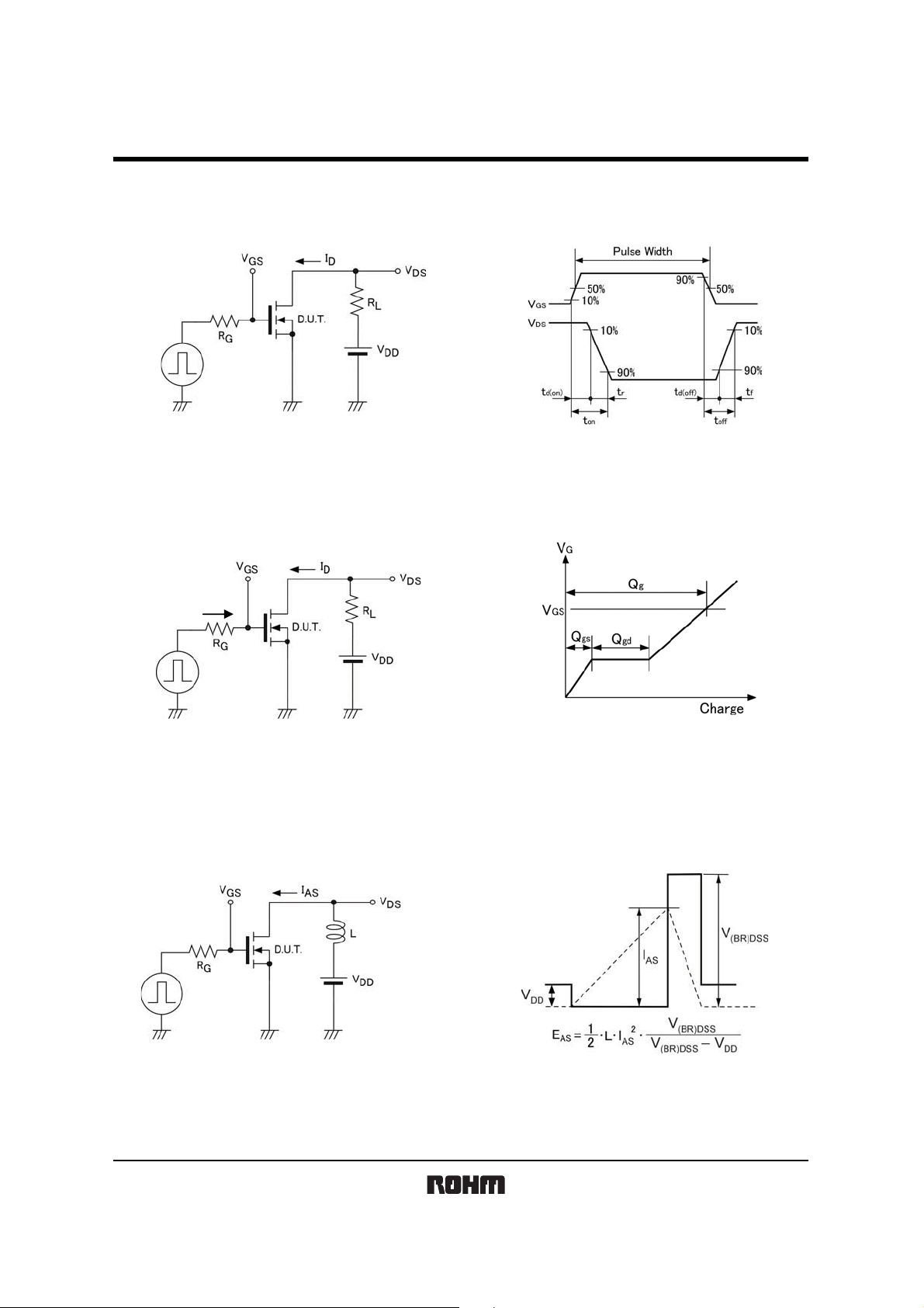
Switching characteristics measurement circuit
Fig.1-1 Switching Time Measurement Circuit! Fig.1-2 Switching Waveforms
IG(Const.)
Fig.2-1 Gate Charge Measurement Circuit! Fig.2-2 Gate Charge Waveform
Fig.3-1 Avalanche Measurement Circuit Fig.3-2 Avalanche Waveform
R5011ANX
5/5
Page 6
Appendix
Notes
No technical content pages of this document may be reproduced in any form or transmitted by any
means without prior permission of ROHM CO.,LTD.
The contents described herein are subject to change without notice. The specifications for the
product described in this document are for reference only. Upon actual use, therefore, please request
that specifications to be separately delivered.
Application circuit diagrams and circuit constants contained herein are shown as examples of standard
use and operation. Please pay careful attention to the peripheral conditions when designing circuits
and deciding upon circuit constants in the set.
Any data, including, but not limited to application circuit diagrams information, described herein
are intended only as illustrations of such devices and not as the specifications for such devices. ROHM
CO.,LTD. disclaims any warranty that any use of such devices shall be free from infringement of any
third party's intellectual property rights or other proprietary rights, and further, assumes no liability of
whatsoever nature in the event of any such infringement, or arising from or connected with or related
to the use of such devices.
Upon the sale of any such devices, other than for buyer's right to use such devices itself, resell or
otherwise dispose of the same, no express or implied right or license to practice or commercially
exploit any intellectual property rights or other proprietary rights owned or controlled by
ROHM CO., LTD. is granted to any such buyer.
Products listed in this document are no antiradiation design.
The products listed in this document are designed to be used with ordinary electronic equipment or devices
(such as audio visual equipment, office-automation equipment, communications devices, electrical
appliances and electronic toys).
Should you intend to use these products with equipment or devices which require an extremely high level
of reliability and the malfunction of which would directly endanger human life (such as medical
instruments, transportation equipment, aerospace machinery, nuclear-reactor controllers, fuel controllers
and other safety devices), please be sure to consult with our sales representative in advance.
It is our top priority to supply products with the utmost quality and reliability. However, there is always a chance
of failure due to unexpected factors. Therefore, please take into account the derating characteristics and allow
for sufficient safety features, such as extra margin, anti-flammability, and fail-safe measures when designing in
order to prevent possible accidents that may result in bodily harm or fire caused by component failure. ROHM
cannot be held responsible for any damages arising from the use of the products under conditions out of the
range of the specifications or due to non-compliance with the NOTES specified in this catalog.
Thank you for your accessing to ROHM product informations.
More detail product informations and catalogs are available, please contact your nearest sales office.
ROHM Customer Support System
www.rohm.com
THE AMERICAS / EUROPE / ASIA / JAPAN
Contact us : webmaster@ rohm.co. jp
Copyright © 2008 ROHM CO.,LTD.
21 Saiin Mizosaki-cho, Ukyo-ku, Kyoto 615-8585, Japan
TEL : +81-75-311-2121
FAX : +81-75-315-0172
Appendix1-Rev2.0
 Loading...