

Datasheet R4430PC-F10-MCM, R4430PC-P10-MCM, R4430SC-1M-F10-MCM Datasheet (Aeroflex Circuit Technology)
Page 1
1
SCD4430 Rev A 11/18/96
The Aeroflex “RISC TurboEngine”
©
A MIPS© R4400 RISC Microprocessor Multichip
Module
Aeroflex Circuit Technology
35 South Service Road, Plainview NY 11803
Tel:(516) 694-6700, Fax:(516) 694-6715
1.0 Description
The Aeroflex Circuit Technology “RISC TurboEngine” is a full military temperature range 64 bit, superpipelined RISC microprocessor with 1M Byte of secondary cache memory packaged in a high speed
multichip module (MCM). The module contains the following components:
• (1) R4400SC/MC, a 3.3V powered RISC microprocessor.
• (11) SRAMs, 64K by 16.
• (3) Buffers and (3) Passive components for phase lock loop operation.
A Primary cache only version, the R4400PC is also available in the same package or 179 pin PGA
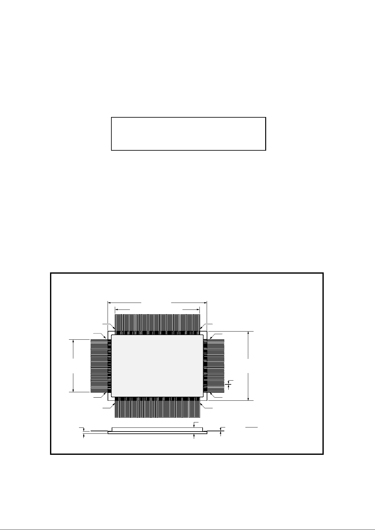
2.0 Flat Package Outline
85 Spaces at 0.025
1.768
MAX
53 Spaces
at 0.025
.010
Pin 226
Pin 141
Pin 227
Pin 140
Pin 87
Pin 86
Pin 280
Pin 1
.006
.175 MAX
.072 ±.01
2.525 MAX
R4400PC/SC
MCM
Note: Outside ceramic tie
bars not shown for clarity.
Contact factory for details
“F10” Package
(Preliminary Data Sheet, use with “MIPS R4000 Microprocessor Users Manual”© MIPS 1993)
Page 2

2
SCD4430 Rev A 11/18/96
3.0 Electrical Features
• Low power dissipation, 3.3 Volt powered, 64 bit superpipelined RISC R4400 microprocessor
- Highly integrated CPU with integer unit, FPA, MMU, I&D cache
- Balanced integer & floating point performance
- Exploits 2-level instruction-level parallelism
- No issue restrictions on the instructions used
• Integer unit
- 32 entry, 64 bit wide register
- ALU
- Dedicated multiplier/divider
• Super pipelined FPA
- 32/16 entry 32/64 bit register file in a 32 bit mode
- 32 entry 64 bit register file in 64 bit mode
- Supports single and double precision.
- Supports ANSI/IEEE Standard 754-1985
• Memory management unit
- 48 entry TLB for fast virtual-to-physical address translation, software managed cntrl regstrs
- Programmable page sizes from 4K bytes to 16M bytes
- Total physical address space encompasses 64G bytes
- One pair of pages per TLB entry, each programable in size from 4K bytes to 16M bytes
• JTAG boundary scan capability for testing module interconnects.
• Internal 1M byte secondary cache SRAM configured as a split cache with instruction and data sections sepa-
rate. Can be factory configured as unified.
• Provides 16 bit ECC on secondary cache data line, 7 bit ECC on tag line.
• Minimum clock rate 50 mHz with no wait states.
• +3.3 Volt P.S.(10 Watts Max.power dissipation) operation is standard.
4.0 Mechanical Features
• Small sizes, 2.5”L X 1.75”W X 0.175”H, 280 pin surface mount flat package or alternate 1.86”LX1.86”W X
0.145”H, 179 pin PGA Package.
• Full military operating temperature range of -55 °C to +125 °C, case temperature
• Designed to meet military specifications, manufactured and tested in Aeroflex’s MIL-PRF-38534 certified
facility.
Page 3
3
SCD4430 Rev A 11/18/96
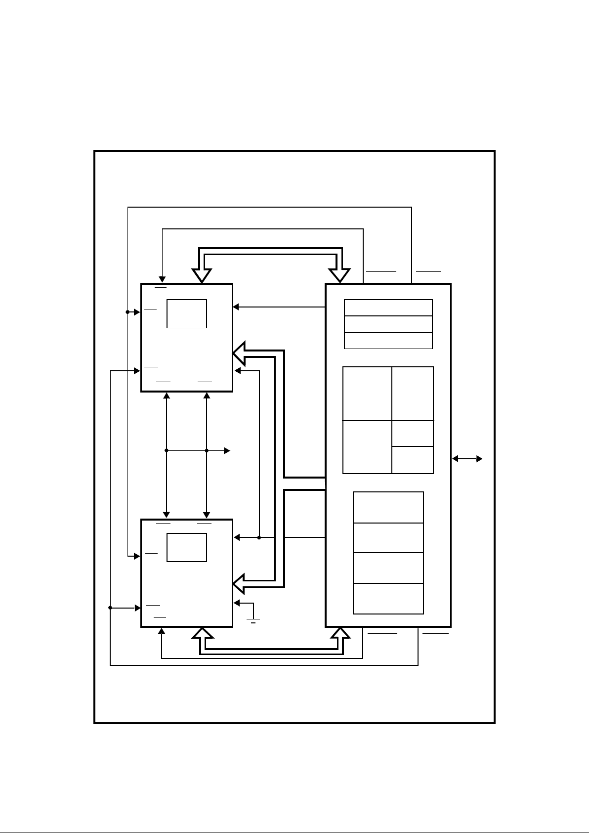
5.0 INTERNAL BLOCK DIAGRAM(SC Version)
General Registers
ALU/Multiply/Divide
Pipeline/Control
INTEGER EXECUTION UNIT
CACHE/MMU
FLOATING POINT
16K Byte
Instruction
Cache
16K Byte
Data
Cache
48 Entry
TLB
Cache
Control
MMU
FPU ALU
Multiply/Divide
Square Root
FP Register
Pipeline Control
SCOESCDCS
SCData(127:0)
SCDchk(15:0)
SCAddr0
SCAddr
SCAddr
17
SCTag(24:0)
SCTchk(6:0)
SCTCS
SCWE
A0
A15
A14:A1
CE
DQ0-DQ31
GND
BW
LBWH
A15
A0
DQ143-DQ0
CE
OE
WE
(9) 64K
by 16
SRAMs
System
Interface
R4400SC/MC Microprocessor
CACHE
CACHE TAG
OE
WE
(14:1)
BW
LBWH
DATA/INSTRUCTION
(2) 64K
by 16
SRAMs
A14:A1
Page 4
4
SCD4430 Rev A 11/18/96
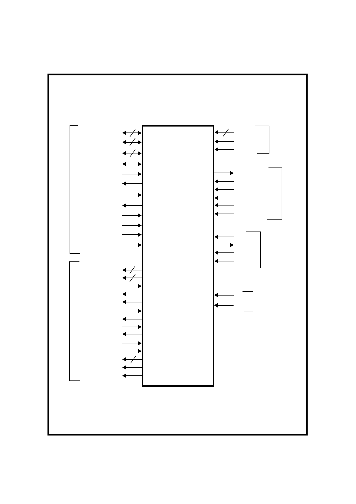
6.0 Module Symbolic Interface Connections
SysAD(63:0)
SysAD(7:0)
SysCmd(8:0)
SysCmdP
ValidIn*
ValidOut*
ExtRqst*
Release*
RdRdy*
WrRdy*
IvdAck* ‡
IvdErr* ‡
TClock(1:0)
RClock(1:0)
MasterClock
MasterOut
SyncOut
SyncIn
IOOut
IOIn
Fault*
VccP
VssP
Status(7:0)
VccSense
System Interface
Clock/Control Interface
Int(5:1)*
Int0*
NMI*
ModeClock
ModeIn
VCCOk
ColdReset*
Reset*
JTDI
JTDO
JTMS
JTCK
VssSense
Interrupt
Interface
Initialization
Interface
JTAG
Interface
64
8
9
2
2
5
R4400
Multichip
Module
8
Vcc
Gnd
Power
Note: Int(5:1)* available on R4400PC version
‡ IvdAck, IvdErr used in “MC” mode
256K/1M*
Page 5

5
SCD4430 Rev A 11/18/96
7.0 Signal Descriptions
System Interface Signals
SysAD(63:0) I/O System address/data bus: A 64 bit address and data
bus for communication between the processor and an
external agent
SysADC(7:0) I/O System address/data check bus: An 8 bit bus contain-
ing check bits for the SysAD bus
SysCmd(8:0) I/O System command/identifier bus parity: A 9 bit bus for
command and data identifier transmission between the
processor and an external agent
SysCmdP I/O System command /data identifier bus parity: A single,
even parity bit for thr SysCmd bus
Validin* I Valid Input: An external agent asserts ValidIn* when it
is driving a valid address or data on the SysAD bus and
a valid command or data identifier on the SysCmd bus
ValidOut* O Valid Output: The processor asserts ValidOut* when it
is driving a valid address or data on the SysAD bus and
a valid command or data identifier on the SYSCMD bus
ExtRqst* I External Request: An external agent asserts ExtRqst* to
request the use of the system interface. The processor
grants the request by asserting Release*
Release* O Release Interface: In response to the assertion of
ExtRqst*, the processor asserts Release* to signal the
requesting device that the system interface is available
RdRdy* I Read ready: The external agent asserts RdRdy*to indi-
cate that it can accept processor read, invalidate, or
update requests in both overlap and non-overlap mode
or can accept a read followed by a potential invalidate
or update request in the overlap mode
WrRdy* I Write ready: An external agent asserts WrRdy* when it
can accept a processor write request
IvdAck* I Invalidate acknowledge: An external agent asserts
IvdAck* to signal successful completion of a processor
invalidate or update request (MC only)
IvdErr* I Invalidate error: An external agent asserts InvErr* to
signal unsuccessful completion of a processor invalidate or update request(MC only)
Page 6

6
SCD4430 Rev A 11/18/96
Clock/Control Interface Signals
TClock(1:0) O Transmit clocks : Two identical transmit clocks that
establish the system interface frequency
RClock(1:0) O Receive clocks: Two identical receive clocks that estab-
lish the system interface frequency
MasterClock I Master clock: Master clock input establishes the pro-
cessor operating frequency
Masterout O Master clock out: Master clock output aligned with
MasterClock
SyncOut O Synchronization clock out: Synchronization clock out-
put must be connected to SyncIn through an interconnect that models the interconnect between MasterOut,
TClock, RClock, and the external agent.
SyncIn I Synchronization clock in: Synchronization clock input
IOOut O I/O output: Output slew rate control feedback loop out-
put. Must be connected to IOIn through a delay loop
that models the I/O path from the processor to an
external agent.
IOIn I I/O input: Output slew rate control feedback loop input
(see IOOut)
Fault* O Fault: The processor asserts Fault to indicate a mis-
match output of boundry comparators
VccP I Quiet Vcc for the PLL: Quiet Vcc for the internal phase
lock loop
VssP I Quiet Vss for the PLL: Quiet Vss for the internal phase
lock loop
Status(7:0) O Status: An 8 bit bus that indicates the current operation
status of the processor
VccSense I/O Vcc sense: This is a special pin used for testing and
characterization. The voltage at this pin directly shows
the behavior of the on chip Vcc.
VssSense I/O Vss sense: VssSense provides a separate, direct connec-
tion fron the on-chip Vss node to a package pin without
attaching to the in-package ground planes. VssSence
should be connected to Vss in functional system
designs.
Page 7

7
SCD4430 Rev A 11/18/96
Interrupt Interface Signals: These signals comprise the interface used by
external agents to interrupt the R4400 processor
Int(5:1)* I Interrupt: Five of six general processor interrupts, bit-
wise ORed with bits 5:1 of the interrupt register. This
feature available on the R4400PC version only
Int0* I Interrupt: One of six general processor interrupts, bit
wise ORed with bit 0 of the interrupt register
NMI* I Nonmaskable interrupt: Nonmaskable interrupt ORed
with bit 6 of the interrupt register
Initialization Interface: These signals comprise the interface by which an
external agent initializes the R4400 operating parameters.
ColdReset* I Cold Reset: This signal must be asserted for a power on
reset or a cold reset. The clocks SClock, TClock, and
RClock begin to cycle and are synchronized with the
de-assertion edge of ColdReset*. ColdReset must be deasserted synchronously with MasterOut.
ModeClock O Boot Mode Clock: Serial boot-mode data clock output
at the system clock frequency divided by 256
ModeIn I Boot mode data in: Serial boot-mode data input.
Reset* I Reset: This signal must be asserted for any reset
sequence. It may be asserted synchronously or asynchronously for a cold reset, or synchronously to initate
a warm reset. Reset must be de-asserted synchronously
with MasterOut.
VccOk I Vcc is OK: When asserted, this signal tells the R4400
that the 3.3 Volt power supply has been above 3.15
Volts for more than 100 milliseconds & will remain stable . Assertion of VccOK starts initialization sequence.
256K/1M* I Cache size Select: Must be connected to ground to
enable the full 1M Byte of cache. Cache size will be
256K if pin is left unconnected.
JTAG Interface Signals
JTDI I JTAG data in: Data is serial, scanned in thru this pin
JTCK I JTAG clock input:The processor outputs a serial clock
on JTCK. On the rising edge of JTCK, both JTDI and
JTMS are sampled.
JTDO O JTAG data out: Data is serial, scanned out thru this pin
JTMS I JTAG: JTAG command signal indicates that the incom-
ming serial data is command clear.
Page 8

8
SCD4430 Rev A 11/18/96
R4400SC/MC Microprocessor Multichip Module Pinouts
Pin # Function Pin # Function Pin # Function
1 TClock 0 48 Vss 95 Vss
2 Vss 49 VssP 96 Sys AD 59
3 Sys AD 45 50 Vcc 97 Vcc
4 Vss 51 IvdAck* 98 Sys AD 27
5 TClock 1 52 Vss 99 Vss
6 Vss 53 VccP 100 IO In
7 Sys AD 13 54 Vcc 101 Vcc
8 Vss 55 Status 5 102 Sys AD 58
9 Sys AD 14 56 Vss 103 Vss
10 Vcc 57 Status 6 104 Sys AD 26
11 JTMS 58 Vcc 105 Vcc
12 Vcc 59 Status 7 106 IO Out
13 Sys AD 46 60 Vcc 107 Vss
14 Vcc 61 Sys ADC 7 108 Sys AD 57
15 JTDO 62 Vcc 109 Vcc
16 Vcc 63 Sys ADC 3 110 Sys AD 25
17 Sys AD 15 64 Vcc 111 Vss
18 Vcc 65 VCC Ok 112 GRPRUN ✪
19 Sys AD 47 66 Vcc 113 Vcc
20 Vss 67 Sys AD 63 114 Sys AD 56
21 Status 0 68 Vss 115 Vss
22 Vcc 69 MasterOut 116 Sys AD 24
23 JTDI 70 Vss 117 Vcc
24 Vss 71 Sys AD 31 118 GRPSTALL ✦
25 Sys ADC 1 72 Vcc 119 Vss
26 Vcc 73 Sys AD 30 120 Sys ADC 6
27 Sys ADC 5 74 Vcc 121 Vcc
28 Vcc 75 Sys AD 62 122 Sys ADC 2
29 Status 2 76 Vss 123 Vss
30 Vcc 77 Sync Out 124 NMI*
31 Status 1 78 Vss 125 Vcc
32 Vcc 79 Sys AD 29 126 Sys AD 55
33 JTCK 80 Vss 127 Vss
34 Vss 81 RClock 1 128 Sys AD 23
35 Sync In 82 Vss 129 Vcc
36 Vss 83 Sys AD61 130 Release *
37 Vss Sense 84 Vss 131 Vss
38 Vss 85 RClock 0 132 Sys AD 22
39 Vcc Sense 86 Vss 133 Vcc
40 Vss 87 Vcc 134 Sys AD 54
41 MasterClock 88 Reset* 135 Vss
42 Vss 89 Vcc 136 Mode In
43 Status 3 90 Sys AD 60 137 Vcc
44 Vcc 91 Vss 138 Rd Rdy *
45 IvdErr* 92 Sys AD 28 139 Vss
46 Vcc 93 Vcc 140 Sys AD 53
47 Status 4 94 Cold_Reset* 141 Sys AD 21
✪ Do not connect, factory test only , ✦ Connect to +V Volts
Page 9

9
SCD4430 Rev A 11/18/96
Pin # Function Pin # Function Pin # Function
142 Vss 189 Int 4* 236 Vss
143 Ext RQST* 190 Vcc 237 Sys Cmd 3
144 Vcc 191 Int 5* 238 Vcc
145 Sys AD 52 192 Vss 239 Sys AD 7
146 Vss 193 Vcc 240 Vss
147 Valid Out* 194 256K/1M* 241 Sys AD 39
148 Vcc 195 SPARE 242 Vcc
149 Sys AD 20 196 SPARE 243 Sys Cmd 4
150 Vss 197 SPARE 244 Vss
151 Sys AD 19 198 CASE GROUND 245 Sys ADC 0
152 Vcc 199 Vss 246 Vcc
153 Sys AD 51 200 Sys AD 32 247 Sys ADC 4
154 Vss 201 Vcc 248 Vss
155 ValidIn* 202 Sys AD 0 249 Sys Cmd 5
156 Vcc 203 Vss 250 Vcc
157 Sys AD 18 204 Sys AD 1 251 Sys AD 8
158 Vss 205 Vcc 252 Vss
159 Sys AD 50 206 Sys AD 33 253 Sys AD 40
160 Vcc 207 Vss 254 Vcc
161 InTO* 208 Sys AD 34 255 Sys Cmd 6
162 Vss 209 Vcc 256 Vss
163 Sys AD 49 210 Sys AD 2 257 Sys AD 9
164 Vcc 211 Vss 258 Vcc
165 Sys AD 17 212 Sys Cmd 0 259 Sys AD 41
166 Vss 213 Vcc 260 Vss
167 Sys AD 16 214 Sys AD 35 261 Sys CMD 7
168 Vcc 215 Vss 262 Vcc
169 Sys AD 48 216 Sys AD 3 263 Sys AD 10
170 Vss 217 Vcc 264 Vss
171 SPARE 218 Sys AD 4 265 Sys AD 42
172 SPARE 219 Vss 266 Vcc
173 SPARE 220 Sys Cmd 1 267 Sys Cmd 8
174 SPARE 221 Vcc 268 Vss
175 SPARE 222 Sys AD 36 269 Sys AD 11
176 SPARE 223 Vss 270 Vcc
177 SPARE 224 Sys Cmd 2 271 Sys AD 43
178 Vss 225 Vcc 272 Vss
179 InT1* 226 Sys AD 5 273 Sys Cmd P
180 Vcc 227 Sys AD 37 274 Vcc
181 InT2* 228 Vss 275 Sys AD 12
182 Vss 229 Mode Clock 276 Vss
183 SPARE 230 Vcc 277 Sys AD 44
184 SPARE 231 WR RDY* 278 Vcc
185 InT3* 232 Vss 279 Fault*
186 SPARE 233 Sys AD 6 280 Vss
187 SPARE 234 Vcc
188 Vss 235 Sys AD 38
R4400SC/MC Microprocessor Multichip Module Pinouts
Page 10

10
SCD4430 Rev A 11/18/96
R4400PC — PGA — Pinouts (See Alternate Package Figure)
Function Pin # Function Pin # Function Pin # Function Pin #
Coldreset
T14 SysAD14 D17 SysAD59 V15 Vcc L18
ExtRqst
U2 SysAD15 EIB SysAD60 T15 Vcc M1
Fault
B16 SysAD16 K2 SysAD61 U17 Vcc N18
Reserved U10 SysAD17 M2 SysAD62 N16 Vcc R1
Vcc T9 Syr.AD18 Pi SysAD63 N17 Vcc T18
IOIn T13 SysAD19 P3 SysADC0 C8 Vcc Ul
IOOut U12 SysAD20 T2 SysADC1 G17 Vcc V3
Int0
N2 SysAD21 T4 SysADC2 T8 Vcc V6
Intl
L3 SysAD22 U5 SysADC3 L16 Vcc V8
Int2
K3 SysAD23 U6 SysADC4 B8 Vcc V10
Int3
J3 SysAD24 U9 SysADC5 H16 Vcc V12
Int4
H3 SysAD25 Ull SysADC6 U8 Vcc V14
lnt5
F2 SysAD26 T12 SysADC7 L17 Vcc V17
JTCK H17 SysAD27 U14 SysCmd0 E2 Vss A3
JTDI G16 SysAD28 U15 SysCmd1 D3 Vss A6
JTDO F16 SysAD29 T16 SysCmd2 B2 Vss A8
JTMS E16 SysAD30 R17 SysCmd3 A5 Vss A10
MasterClock J17 SysAD31 M16 SysCmd4 B7 Vss A12
MasterOut P17 SysAD32 H2 SysCmd5 C9 Vss A14
ModeClock B4 SysAD33 G3 SysCmd6 B10 Vss A17
ModeIn U4 SysAD34 F3 SysCmd7 B12 Vss A18
NMI
U7 SysAD35 D2 SysCmd8 C13 Vss B1
PLLCap0 .... SysAD36 C3 SysCmd9 C14 Vss C18
PLLCap1 .... SysAD37 B3 TClock0 C17 Vss D1
RClock0 T17 SysAD38 C6 TClockl D16 Vss F18
RClockl R16 SysAD39 C7 VCCOk M17 Vss GI
RdRdy
T5 SysAD40 C10 ValidIn P2 Vss H18
Release
V5 SysAD41 C11 ValidOut R3 Vss J1
Reset
U16 SysAD42 B13 WrRdy C5 Vss K18
SyncIn J16 SysAD43 A15 VccP K17 Vss Ll
SyncOut P16 SysAD44 C15 VssP K16 Vss M18
SysADO J2 SysAD45 B17 Vcc A2 Vss Nl
SysAD1 G2 SysAD46 E17 Vcc A4 Vss P18
SysAD2 El SysAD47 F17 Vcc A9 Vss R18
SysAD3 E3 SysAD48 L2 Vcc A11 Vss Tl
SysAD4 C2 SysAD49 M3 Vcc A13 Vss U18
SysAD5 C4 SysAD50 N3 Vcc A16 Vss V1
SysAD6 B5 SysAD51 R2 Vcc B18 Vss V2
SysAD7 B6 SysAD52 T3 Vcc C1 Vss V4
SysAD8 B9 SysAD53 U3 Vcc D18 Vss V7
SysAD9 B11 SysAD54 T6 Vcc Fl Vss V9
SysAD10 C12 SysAD55 T7 Vcc G18 Vss V11
SysAD11 B14 SysAD56 T10 Vcc Hl Vss V13
SysAD12 B15 SysAD57 T11 Vcc J18 Vss V16
SysAD13 C16 SysAD58 U13 Vcc K1 Vss V18
Page 11

11
SCD4430 Rev A 11/18/96
ORDERING INFORMATION
Microprocessor Module Description Part Number
R4430 Primary Cache, +3.3 Volt P.S. Flat Package R4430PC F10 MCM
R4430 Primary Cache, +3.3 Volt P.S. PGA Package R4430PC P10 MCM
R4430 1Meg Secondary Cache, +3.3 Volt P.S. Flat Package R4430SC 1M F10 MCM
1.840
1.880
1.700
BSC
1.700
BSC
1.840
1.880
BSC
.100
.221
MAX
V
U
T
R
P
N
M
L
K
J
H
G
F
E
D
C
B
A
1 2 3 4 5 6 7 8 9 10 11 12 13 14 15 16 17 18
Bottom View
Side View
Alternate Package Figure — R4400PC — PGA 179 Pins
Specification subject to change without notice
“P10” Package
.018
.050
 Loading...