

Page 1

R2045S/D
4-wire Serial Interface Real Time Clock Module
NO.EA-113-100825
OUTLINE
The R2045S/D is a real-time clock module, built in CMOS real-time clock IC and crystal oscillator, connected to
the CPU by four signal lines, CE, SCLK, SI, and SO, and configured to perform serial transmission of time and
calendar data to the CPU. The oscillation frequency is adjusted to high precision (0±5ppm: 15sec. per month at
25°C) The periodic interrupt circuit is configured to generate interrupt signals with six selectable interrupts
ranging from 0.5 seconds to 1 month. The 2 alarm interrupt circuits generate interrupt signals at preset times. As
the oscillation circuit is driven under constant volt age, fluctuation of the oscillator frequency due to supply volt age
is small, and the time keeping current is small (TYP. 0.48μA at 3V). The oscillation halt sensing circuit can be
used to judge the validity of internal data in such events as power-on; The supply voltage monitoring circuit is
configured to record a drop in supply voltage below two selectable supply voltage monitoring threshold settings.
The 32-kHz clock output function (N-channel Open drain output) is intended to output sub-clock pulses for the
external microcomputer. The oscillation adjustment circuit is intended to adjust time by correcting deviations in
the oscillation frequency of the crystal oscillator.
FEATURES
• Built in 32.768kHz crystal unit, The oscillation frequency is adj usted to high precision (0±5ppm: at 25°C)
• Time keeping voltage 1.15V to 5.5V
• Super low power consumption 0.48μA TYP (1.2μA MAX) at V
• Four signal lines (CE, SCLK, SI, and SO) required for connection to the CPU.
• Time counters (counting hours, minutes, and seconds) and calendar counters (counting years, months,
days, and weeks) (in BCD format)
• Interrupt circuit configured to generate interrupt signals (with interrupts ranging from 0.5 seconds to 1
month) to the CPU and provided with an interrupt flag and an interrupt halt
• 2 alarm interrupt circuits (Alarm_W for week, hour, and minute alarm settings and Alarm_D for hour and
minute alarm settings)
• 32768Hz clock output pin (N-channel open drain output)
• With Power-on flag to prove that the power supply starts from 0V
• With Oscillation halt sensing Flag to judge the validity of internal data
• Supply voltage monitoring circuit with two supply voltage monitoring threshold settings
• Automatic identification of leap years up to the year 2099
• Selectable 12-hour and 24-hour mode settings
• Oscillation adjustment circuit for correcting temperature frequency deviation or offset deviation
• CMOS process
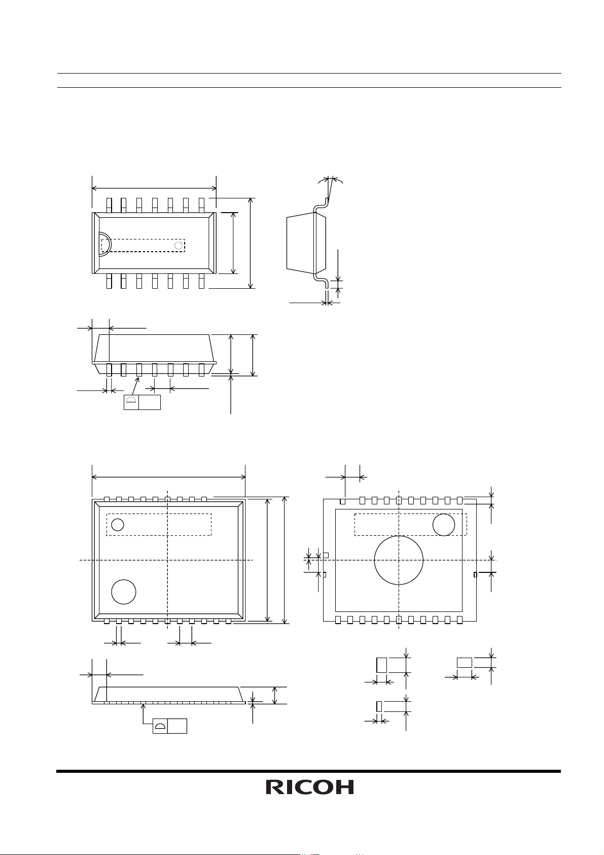
• Two types of p ackage, SOP14(10.1x7.4x3.1) or SON22(6.1x5.0x1.3)
DD=3V
1
Page 2
R2045S/D
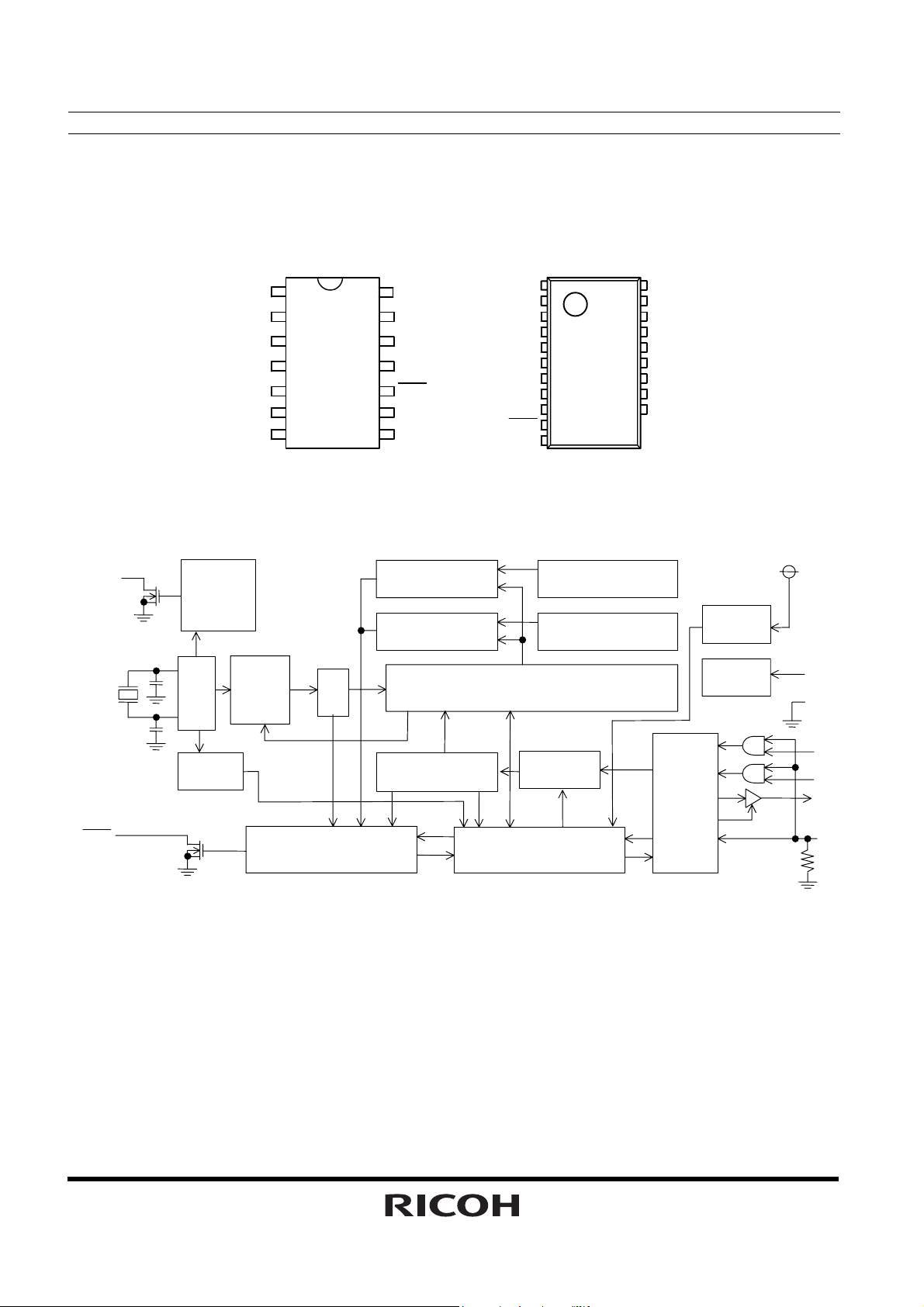
PIN CONFIGURATION
32KOUT
R2045S (SOP14)
N.C.
SCLK SO
N.C.
VPP
VDD N.C.
1
2
3
4
5
6
7
TOP VIEW
BLOCK DIAGRAM
14
13
12
11
10
N.C.
SI
VSS
INTR
9
N.C. CE
8
R2045D (SON22)
CE
1
VDD
2
N.C. N.C.
3
VPP
SO
VSS
INTR
N.C.
4
5
6
7
SI
8
9
10
11
32KOUT
SCLK
TOP VIEW
22
21
20
19
18
17
16
15
14
N.C.
N.C.
N.C.
N.C.
N.C.
N.C.
N.C.
N.C.
32KOUT
INTR
32kHz
OUTPUT
CONTROL
OSC
OSC
DETECT
DIVIDER
CORREC
-TION
INTERRUPT CONTROL
DIV
COMPARATOR_W
COMPARATOR_D
(SEC,MIN,HOUR,WEEK,DAY,MONTH,YEAR)
ADDRESS
DECODER
TIME COUNTER
SHIFT REGISTER
ALARM_W REGISTER
(MIN,HOUR, WEEK)
ALARM_D REGISTER
(MIN,HOUR)
ADDRESS
REGISTER
I/O
CONTROL
VOLTAGE
DETECT
TEST
CIRCUIT
VDD
VPP
VSS
SCLK
SI
SO
CE
2
Page 3

PIN DESCRIPTION
Symbol Item Description
CE Chip enable
Input
SCLK Serial Clock
Input
SI Serial Input The SI pin is used to input data intended for writing in synchronization with
SO Serial
Output
INTR
32KOUT 32kHz Clock
VDD Positive
VSS Negative
VPP Test input This pin is power pin for testing in the factory. Please don’t connect to any
N.C. No
Interrupt
Output
Output
Power
Supply Input
Power
Supply Input
Connection
The CE pin is used for interfacing with the CPU. Should be held high to
allow access to the CPU. Incorporates a pull-down resistor. Should be
held low or open when the CPU is powered off. Allows a maximum input
voltage of 5.5v regardless of supply voltage.
The SCLK pin is used to input clock pulses synchronizing the input and
output of data to and from the SI and SO pins. Allows a maximum input
voltage of 5.5v regardless of supply voltage.
the SCLK pin. CMOS input. Allows a maximum input voltage of 5.5v
regardless of supply voltage.
The SO pin is used to output data intended for reading in synchronization
with the SCLK pin. CMOS output.
INTR
The
interrupt (Alarm_D) and output periodic interrupt signals to the CPU sign als.
Disabled at power-on from 0V. N-channel open drain output. Allows a
maximum pull-up voltage of 5.5v regardless of supply voltage.
The 32KOUT pin is used to output 32.768-kHz clock pulses. And controlled
by resister setting. When VDD power-on from 0v, this output is enabled.
The pin is N-channel open drain output. Allows a maximum pull-up voltage
of 5.5v regardless of supply voltage.
The VDD pin is connected to the power supply.
The VSS pin is grounded.
other pins.
These pins are not connected to internal IC chip.
In R2045D (SON22), N.C. pins from 14 pin to 22 pin are connected together
internally. Never connect these pins to any lines, or connect to VDD or
VSS. And never connect different voltage level lines each other.
pin is used to output alarm interrupt (Alarm_W) and alarm
R2045S/D
3
Page 4
R2045S/D
ABSOLUTE MAXIMUM RATINGS
(VSS=0V)
Symbol Item Pin Name and Condition Description Unit
VDD Supply Voltage VDD -0.3 to +6.5 V
Input Voltage 1 CE, SCLK, SI -0.3 to +6.5 VI
Input Voltage 2 VPP -0.3 to V
Output Voltage 1 SO -0.3 to VDD+0.3 VO
Output Voltage 2
PD Power Dissipation
Topt Operating
Temperature
Tstg Storage Temperature -55 to +125
INTR
, 32KOUT
Topt=25°C
-40 to +85
-0.3 to +6.5
300 mW
DD+0.3
V
V
°C
°C
RECOMMENDED OPERATING CONDITION
(VSS=0V, Topt=-40 to +85°C)
Symbol Item Pin Name and Condition Min. Typ. Max. Unit
VACCESS Supply Voltage VDD power supply voltage
for interfacing with CPU
VCLK Time Keeping Voltage 1.15 5.5 V
VPUP Pull-up Voltage
INTR
1.7 5.5 V
5.5 V
FREQUENCY CHARACTERISTICS
(VSS=0V)
Symbol Item Condition Min. Typ. Max. Unit
Δf/f0
Fv Frequency
Top Frequency
tsta Oscillation
fa Aging
Frequency
Deviation
Voltage
Characteristics
Temperature
Characteristics
Start-up Time
Topt=25°C, VDD=3V
Topt=25°C,
DD=2.0V to 5.5V
V
Topt=-20°C to +70°C
25°C as standard
Topt=25°C, V
Topt=25°C, V
First year
DD=2V
DD=3V,
-5 0 +5 ppm
-1 +1 ppm
-120 +10 ppm
+1 sec
-5 +5 ppm
4
Page 5
R2045S/D
DC ELECTRICAL CHARACTERISTICS
Unless otherwise specified: VSS=0V,VDD=3V,Topt=-40 to +85°C
Symbol Item Pin Name Condition Min. Typ. Max. Unit
VIH “H” Input Voltage 0.8x
CE,
DD=1.7 to 5.5V
V
SCLK,
VIL “L” Input Voltage
IOH “H” Output
SI
SO VOH=VDD-0.5V -0.5 mA
Current
IOL1
IOL2
“L” Output Current
INTR
SO,
OL=0.4V
V
32KOUT
IIL Input Leakage
Current
RDNCE Pull-down
SCLK, SI VI=5.5V or VSS
DD=5.5V
V
CE 40 120 400
Resistance
IOZ1 SO VO=5.5V or VSS
IOZ2
IDD1
Output Off-state
Leakage Current
Time Keeping
Current
INTR
,
32KOUT
VDD
VDD=5.5V
VO=5.5V
VDD=3V,
CE, SCLK, SI, SO,
INTR
, 32KOUT
SS
=V
32KOUT disabled
IDD2
VDD
VDD=5V,
CE, SCLK, SI, SO,
INTR
, 32KOUT
SS
=V
32KOUT disabled
IDD3
VDD VDD=3V,
CE, SCLK, SI, SO,
INTR
, 32KOUT
SS
=V
32KOUT enabled
V
V
DETH
DETL
Supply Voltage
Monitoring Voltage
(“H”)
Supply Voltage
Monitoring Voltage
(“L”)
VDD
VDD
Topt=-30 to +70°C
Topt=-30 to +70°C
DD
V
-0.3 0.2x
2.0
0.5
-1.0 1.0
-1.0 1.0
-1.0 1.0
0.65 2.00
1.90
1.15
5.5
DD
V
0.48 1.20
0.60 1.80
2.10 2.30
1.30 1.45
V
mA
μA
kΩ
μA
μA
V
V
5
Page 6
R2045S/D
K
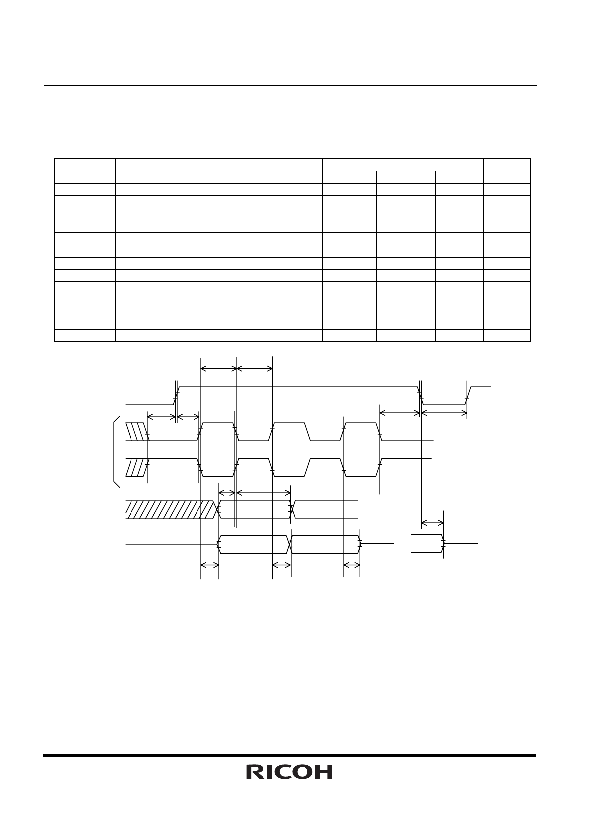
AC ELECTRICAL CHARACTERISTICS
Unless otherwise specified: VSS=0V,Topt=-40 TO +85°C
Input / Output condition: V
Symbol Item Condi-
t
CE Set-up Time 400 ns
CES
t
CE Hold Time 400 ns
CEH
tCR CE Recovery Time 62
f
SCLK Clock Frequency 1.0 MHz
SCLK
t
SCLK Clock High Time 400 ns
CKH
t
SCLK Clock Low Time 400 ns
CKL
t
SCLK Set-up Time 200 ns
CKS
tRD Data Output Delay Time 300 ns
tRZ Data Output Floating Time 300 ns
t
Data Output Delay Time
CEZ
After Falling of CE
tDS Input Data Set-up Time 200 ns
tDH Input Data Hold Time 200 ns
IH=0.8xVDD,VIL=0.2xVDD,VOH=0.8xVDD,VOL=0.2xVDD,CL=50pF
V
DD≥1.7V
tions
Min. Typ. Max.
300 ns
t
CKH
t
CKL
Unit
μs
CE
t
CKS
SCL
SI
SO
*) For reading/writing timing, see “P.
condition”.
t
CES
t
CEH
t
CEZ
tCR
t
DS
t
DH
tRD
t
RD
t
RZ
26 •Considerations in Reading and W riting Time Data under special
6
Page 7
#
#7 #1 #
A
A
A
A
PACKAGE DIMENSIONS
• R2045S (SOP14)
1.24typ.
10.1±0.2
0.1
±
6.1
1.27±0.1
0.2
8
5.0±0.2
7.4±0.2
0.1
±
3.2
3.1typ.
-0.05
+0.1
0.1
14
+0.1
0.35
-0.05
• R2045D (SON22)
#22 #14
0°-10
0.15
°
+0.1
-0.05
0.65
0.25
±
0.6
R2045S/D
#22 #14
’
0.1
±
0.3
5.0
0.05
B
0.43
’
0.2
0.1
±
B
0.3
B
0.43
#1 #11
0.3
0.2
0.1
0.2
0.2
0.2
±
±
4.7
0.1
0.2
±
0.5
0.1
±
#1 #11
0.55typ.
1.3
+0.1/-0.05
0.125
0.1
7
Page 8

R2045S/D
GENERAL DESCRIPTION
• Interface with CPU
The R2045S/D is connected to the CPU by four signal lines CE (Chip Enable), S CLK (Serial Clock), SI (Serial
Input), and SO (Serial Output), through which it reads and writes data from and to the CPU. The CPU can be
accessed when the CE pin is held high. Access clock pulses have a maximum frequency of 1 MHz allowing
high-speed data transfer to the CPU.
• Clock and Calendar Function
The R2045S/D reads and writes time data from and to the CPU in units ranging from seconds to the last two
digits of the calendar year. The calendar year will automatically be identified as a leap year when its last two
digits are a multiple of 4. Consequently , leap years u p to the year 2099 can automatically be identified as such.
• Alarm Function
The R2045S/D incorporates the alarm interrupt circuit configured to generate interrupt signals to the CPU at
preset times. The alarm interrupt circuit allows two types of alarm settings specified by the Alarm_W registers
and the Alarm_D registers. The Alarm_W registers allow week, hour, and minute alarm settings including
combinations of multiple day-of-week settings such as "Monday, Wednesday, and Friday" and "Saturday and
Sunday". The Alarm_D registers allow hour and minute alarm settings. The Alarm_W outputs from
pin, and the Alarm_D output s also from
a polling function.
INTR
pin. Each alarm function can be checked from the CPU by using
High-precision Oscillation Adjustment Function
INTR
To correct deviations in the oscillation frequency of the crystal oscillator, the oscillation adjustment circuit is
configured to allow correction of a time count gain or loss (up to ±1.5 ppm at 25°C) from the CPU within a
maximum range of approximately + 189 ppm in increments of approximately 3 ppm. Such oscillation frequen cy
adjustment in each system has the following advantages:
* Corrects seasonal frequency deviations through seasonal o scillation adjustment.
* Allows timekeeping with higher precision particularly with a temperature sensing function out of RTC,
through oscillation adjustment in tune with temperature fluctuations.
• Oscillation Halt Sensing Flag, Power-on Reset Flag, and Supply Voltage Monitoring Function
The R2045S/D incorporates an oscillation halt sensing circuit equipped with internal registers configured to
record any past oscillation halt.
Power-on reset flag is set to “1” When R2045S/D is powered on from 0V.
As such, the oscillation halt sensing flag and Power-on reset flag are useful for judging the validity of time
data.
The R2045S/D also incorporates a supply voltage monitoring circuit equipped with internal registers
configured to record any drop in supply voltage below a certain threshold value. Supply voltage monitoring
threshold settings can be selected between 2.1 and 1.3 volts through internal register settings. The oscillation
halt sensing circuit is configured to confirm the established invalidation of time data in contrast to the supply
voltage monitoring circuit intended to confirm the potential invalidation of time data. Further, the supply voltage
monitoring circuit can be applied to battery supply voltage monitoring.
8
Page 9

R2045S/D
• Periodic Interrupt Function
The R2045S/D incorporates the periodic interrupt circuit configured to generate periodic interrupt signals
aside from interrupt signals generated by the periodic interrupt circuit for output from the
interrupt signals have five selectable frequency settings of 2 Hz (once per 0.5 seconds), 1 Hz (once per 1
second), 1/60 Hz (once per 1 minute), 1/3600 Hz (once per 1 hour), and monthly (the first day of every month).
Further, periodic interrupt signals also have two selectable waveforms, a normal pulse form (with a frequency of
2 Hz or 1 Hz) and special form adapted to interruption from the CPU in the level mode (with second, minute, hour,
and month interrupts). The condition of periodic interrupt signals can be monitored by using a polling function.
INTR
pin. Periodic
• 32kHz Clock Output
The R2045S/D incorporates a 32-kHz clock circuit configured to generate clock pulses with the oscillation
frequency of a 32.768kHz crystal oscillator for output from the 32KOUT pin. The 32-kHz clock output can be
disabled by certain register settings but cannot be disabled without manipulation of any two registers with
different addresses to prevent disabling in such event s as the runaway of the CPU.
9
Page 10
R2045S/D
A
A
A
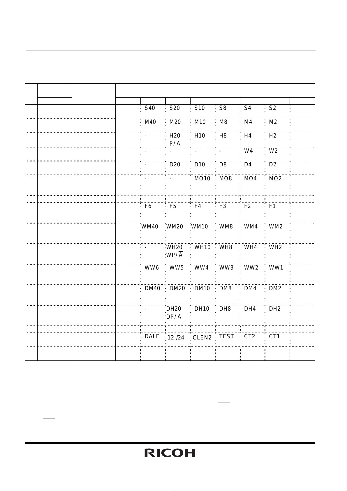
Address Mapping
Address Register
Name
A3A2A1A0 D7 D6 D5 D4 D3 D2 D1 D0
0 0 0 0 0 Second
Counter
1 0 0 0 1 Minute
Counter
2 0 0 1 0 Hour Counter - - H20
3 0 0 1 1 Day-of-week
Counter
4 0 1 0 0 Day-of-month
Counter
5 0 1 0 1 Month
Counter and
Century Bit
6 0 1 1 0 Year Counter Y80 Y40 Y20 Y10 Y8 Y4 Y2 Y1
7 0 1 1 1 Oscillation
Adjustment
Register *3)
8 1 0 0 0 Alarm_W
(Minute
Register)
9 1 0 0 1 Alarm_W
(Hour
Register)
A 1 0 1 0 Alarm_W
(Day-of-week
Register)
B 1 0 1 1 Alarm_D
(Minute
Register)
C 1 1 0 0 Alarm_D
(Hour
Register)
D 1 1 0 1 - - - - - - - E 1 1 1 0 Control
Register 1 *3)
F 1 1 1 1 Control
Register 2 *3)
Notes:
*1) All the data listed above accept both reading and writing.
*2) The data marked with "-" is invalid for writing and reset to 0 for reading.
*3) When the PON bit is set to 1 in Control Register 2, all the bits are reset to 0 in Oscillation Adjustment
Register, Control Register 1 and Control Register 2 excluding the
*4) The (0) bit should be set to 0.
XST
*5)
*6) PON is power-on reset flag.
is oscillation halt sensing bit.
*2)
- M40 M20 M10 M8 M4 M2 M1
- - - - - W4 W2 W1
- - D20 D10 D8 D4 D2 D1
19
/20
(0)
*4)
- WM40 WM20 WM10 WM8 WM4 WM2 WM1
- - WH20
- WW6 WW5 WW4 WW3 WW2 WW1 WW0
- DM40 DM20 DM10 DM8 DM4 DM2 DM1
- - DH20
WALE DALE
VDSL VDET
S40 S20 S10 S8 S4 S2 S1
P/
- - MO10 MO8 MO4 MO2 MO1
F6 F5 F4 F3 F2 F1 F0
12
/24
XST
WP/
DP/
D a t a
H10 H8 H4 H2 H1
WH10 WH8 WH4 WH2 WH1
DH10 DH8 DH4 DH2 DH1
CLEN2
PON
*5)
TEST CT2 CT1 CT0
CLEN1
XST
CTFG WAFG DAFG
and PON bits.
10
Page 11
R2045S/D
Register Settings
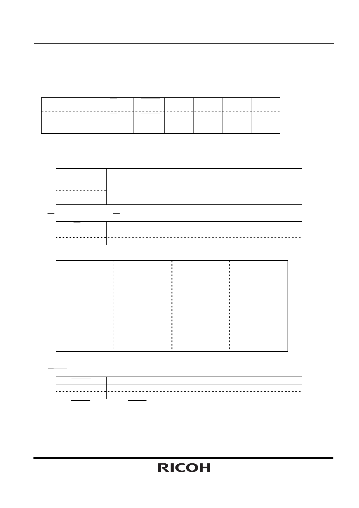
• Control Register 1 (ADDRESS Eh)
D7 D6 D5 D4 D3 D2 D1 D0
WALE DALE
WALE DALE
0 0 0 0 0 0 0 0 Default Settings *)
*) Default settings: Default value means read / written values when the PON bit is set to “1” due to VDD
power-on from 0 volts.
12
12
/24
/24
CLEN2
CLEN2
(1) WALE, DALE Alarm_W Enable Bit, Alarm_D Enable Bit
WALE,DALE Description
0 Disabling the alarm interrupt circuit (under the control of the settings
of the Alarm_W registers and the Alarm_D registers).
1 Enabling the alarm interrupt circuit (under the control of the settings
of the Alarm_W registers and the Alarm_D registers)
12
(2)
(3)
/24
12
/24
0 Selecting the 12-hour mode with a.m. and p.m. indications. (Default)
1 Selecting the 24-hour mode
Setting the
24-hour mode 12-hour mode 24-hour mode 12-hour mode
00 12 (AM12) 12 32 (PM12)
01 01 (AM 1) 13 21 (PM 1)
02 02 (AM 2) 14 22 (PM 2)
03 03 (AM 3) 15 23 (PM 3)
04 04 (AM 4) 16 24 (PM 4)
05 05 (AM 5) 17 25 (PM 5)
06 06 (AM 6) 18 26 (PM 6)
07 07 (AM 7) 19 27 (PM 7)
08 08 (AM 8) 20 28 (PM 8)
09 09 (AM 9) 21 29 (PM 9)
10 10 (AM10) 22 30 (PM10)
11 11 (AM11) 23 31 (PM11)
Setting the
CLEN2
0 Enabling the 32-kHz clock output (Default)
1 Disabling the 32-kHz clock output
Setting the
pulses with the oscillation frequency of the 32.768-kHz crystal oscillator for output from the 32KOUT pin.
Conversely, setting both the
12
/24 bit to 0 and 1 specifies the 12-hour mode and the 24-hour mode, respectively.
12
/24 bit should precede writing time data
32-kHz Clock Output Bit2
CLEN2
CLEN2
bits or the
12
/24-hour Mode Selection Bit
CLEN1
CLEN1
bit (D3 in the control register 2) to 0 specifies generating clock
and the
TEST CT2 CT1 CT0 (For Writing)
TEST CT2 CT1 CT0 (For Reading)
Description
Description
CLEN2
bit to 1 specifies disabling (“H”) such output.
(Default)
11
Page 12
R2045S/D
A
(4) TEST Test Bit
TEST Description
0 Normal operation mode. (Default)
1 Test mode.
The TEST bit is used only for testing in the factory and should normally be set to 0.
(5) CT2,CT1, and CT0 Periodic Interrupt Selection Bits
Description CT2 CT1 CT0
Wave form
mode
0 0 0 - OFF(H) (Default)
0 0 1 - Fixed at “L”
0 1 0 Pulse Mode
*1)
0 1 1 Pulse Mode
*1)
1 0 0 Level Mode
*2)
1 0 1 Level Mode
*2)
1 1 0 Level Mode
*2)
1 1 1 Level Mode
*2)
* 1) Pulse Mode: 2-Hz and 1-Hz clock pulses are output in synchronization with the increment of the
second counter as illustrated in the timing chart below.
Interrupt Cycle and Falling Timing
2Hz(Duty50%)
1Hz(Duty50%)
Once per 1 second (Synchronized with
second counter increment)
Once per 1 minute (at 00 seconds of
every minute)
Once per hour (at 00 minutes and 00
seconds of every hour)
Once per month (at 00 hours, 00 minutes,
and 00 seconds of first day of every
month)
12
In the pulse mode, the increment of the second counter is delayed by approximately 92 μs from the falling
edge of clock pulses. Consequently, time readings immediately after the falling edge of clock pulses may
appear to lag behind the time counts of the real-time clocks by approximately 1 second. Rewriting the
second counter will reset the other time counters of less than 1 second, driving the
* 2) Level Mode: Periodic interrupt signals are output with selectable interrupt cycle settings of 1 second,
1 minute, 1 hour, and 1 month. The increment of the second counter is synchronized with the falling edge
of periodic interrupt signals. For example, periodic interrupt signals with an interrupt cycle setting of 1
second are output in synchronization with the increment of the second counter as illustrated in the timing
chart below.
CTFG Bit
IN T R
Pin
pprox. 92μs
(Increment of second counter)
INTR
pin low.
Rewriting of the second counter
Page 13

R2045S/D
*1), *2) When the oscillation adjustment circuit is used, the interrupt cycle will fluctuate once per 60sec. as
follows:
Pulse Mode:
The “L” period of output pulses will increment or decrement by a maximum of ±3.784 ms. For example,
1-Hz clock pulses will have a duty cycle of 50 ±0.3784%.
Level Mode:
A periodic interrupt cycle of 1 second will increment or decrement by a maximum of ±3.784 ms.
CTFG Bit
IN T R
Pin
(Increment of
second counter)
Setting CTFG bit to 0
(Increment of
second counter)
Setting CTFG bit to 0
(Increment of
second counter)
• Control Register 2 (Address Fh)
D7 D6 D5 D4 D3 D2 D1 D0
VDSL VDET
VDSL VDET
0 0
*) Default settings: Default value means read / written values when the PON bit is set to “1” due to VDD
power-on from 0 volts.
XST
XST
Indefinite
PON
PON
1 0 0 0 0 Default Settings *)
CLEN1
CLEN1
(1) VDSL VDD Supply Voltage Monitoring Threshold Selection Bit
VDSL Description
0 Selecting the VDD supply voltage monitoring threshold setting of 2.1v. (Default)
1 Selecting the VDD supply voltage monitoring threshold setting of 1.3v.
The VDSL bit is intended to select the VDD supply voltage monitoring threshold settings.
(2) VDET Supply Voltage Monitoring Result Indication Bit
VDET Description
0 Indicating supply voltage above the supply voltage monitoring
threshold settings.
1 Indicating supply voltage below the supply voltage monitoring
threshold settings.
Once the VDET bit is set to 1, the supply voltage monitoring circuit will be disabled while the VDET bit will
hold the setting of 1. The VDET bit accepts only the writing of 0, which restarts the supply voltage
monitoring circuit. Conversely, setting the VDET bit to 1 causes no event.
XST
(3)
Oscillation Halt Sensing Monitor Bit
XST
0 Sensing a halt of oscillation
1 Sensing a normal condition of oscillation
CTFG WAF
G
CTFG WAF
G
Description
DAFG (For Writing)
DAFG (For Reading)
(Default)
13
Page 14

R2045S/D
XST
The
halt sensing. The
accepts the reading and writing of 0 and 1. The
XST
bit will hold 0 even after the restart of oscillation.
(4) PON Power-on-reset Flag Bit
PON Description
0 Normal condition
1 Detecting VDD power-on -reset (Default)
The PON bit is for sensing power-on reset condition.
* The PON bit will be set to 1 when VDD power-on from 0 volts. The PON bit will hold the setting of 1 even
after power-on.
* When the PON bit is set to 1, all bits will be reset to 0, in the Oscillation Adjustment Register, Control
Register 1, and Control Register 2, except
32KOUT starts outputting.
* The PON bit accepts only the writing of 0. Conversely, setting the PON bit to 1 causes no event.
CLEN1
(5)
Setting the
pulses
with the oscillation frequency of the 32.768-kHz crystal oscillator for output from the 32KOUT pin.
Conversely, setting both the
32-kHz Clock Output Bit 1
CLEN1
0
1
CLEN1
Enabling the 32-kHz clock output
Disabling the 32-kHz clock output
bit or the
CLEN2
CLEN1
XST
and PON. As a result,
Description
bit (D4 in the control register 1) to 0 specifies generating clock
and the
CLEN2
(6) CTFG Periodic Interrupt Flag Bit
CTFG Description
0 Periodic interrupt output = “H” (Default)
1 Periodic interrupt output = “L”
The CTFG bit is set to 1 when the periodic interrupt signals are output from the
CTFG bit accepts only the writing of 0 in the level mode, which disables (“H”) the
enabled (“L”) again in the next interrupt cycle. Conversely, setting the CTFG bit to 1 causes no event.
(7) WAFG,DAFG Alarm_W Flag Bit and Alarm_D Flag Bit
WAFG,DAFG Description
0 Indicating a mismatch between current time and preset alarm time (Default)
1 Indicating a match between current time and preset alarm time
The WAFG and DAFG bits are valid only when the WALE and DALE have the setting of 1, which is caused
approximately 61μs after any match between current time and preset alarm time specified by the Alarm_W
registers and the Alarm_D registers. The WAFG (DAFG) bit accepts only the writing of 0.
outputs off (“H”) when this bit is set to 0. And
Conversely, setting the WAFG and DAFG bits to 1 causes no event. The WAFG and DAFG bits will have
the reading of 0 when the alarm interrupt circuit is disabled with the WALE and DALE bits set to 0.
The settings of the WAFG (DAFG) bit is synchronized with the output of the
timing chart below.
INTR
pin outputs “L” again at the next preset alarm time.
XST
bit will be set to 0 when the oscillation
INTR
pin stops outputting, and
(Default)
bit to 1 specifies disabling (“H”) such output.
INTR
pin (“L”). The
INTR
pin until it is
INTR
pin
INTR
pin as shown in the
14
Page 15
R2045S/D
A
A
A
A
pprox. 61μs
pprox. 61μs
WAFG(DAFG) Bit
INTR Pin
Writing of 0 to
WAFG(DAFG) bit
(Match between
current time and
preset alarm time)
(Match between
current time and
preset alarm time)
Writing of 0 to
WAFG(DAFG) bit
(Match between
current time and
preset alarm time)
• Time Counter (Address 0-2h)
Second Counter (Address 0h)
D7 D6 D5 D4 D3 D2 D1 D0
- S40 S20 S10 S8 S4 S2 S1 (For Writing)
0 S40 S20 S10 S8 S4 S2 S1 (For Reading)
0 Indefi
nite
Minute Counter (Address 1h)
D7 D6 D5 D4 D3 D2 D1 D0
- M40 M20 M10 M8 M4 M2 M1 (For Writing)
0 M40 M20 M10 M8 M4 M2 M1 (For Reading)
0 Indefi
nite
Hour Counter (Address 2h)
D7 D6 D5 D4 D3 D2 D1 D0
- -
0 0
0 0 Indefi
*) Default settings: Default value means read / written values when the PON bit is set to “1” due to VDD
power-on from 0 volts.
* Time digit display (BCD format) as follows:
The second digits range from 00 to 59 and are carried to the minute digit in transition from 59 to 00.
The minute digits range from 00 to 59 and are carried to the hour digits in transition from 59 to 00.
The hour digits range as shown in "P
Mode Selection Bit" and are carried to the day-of-month and day-of-week digits in tran sition from PM11 to
AM12 or from 23 to 00.
Indefi
nite
Indefi
nite
P/
or
H20
P/
or
H20
nite
Indefi
nite
Indefi
nite
H10 H8 H4 H2 H1 (For Writing)
H10 H8 H4 H2 H1 (For Reading)
Indefi
nite
11 •Control Register 1 (ADDRESS Eh) (2)
Indefi
nite
Indefi
nite
Indefi
nite
Indefi
nite
Indefi
nite
Indefi
nite
Indefi
nite
Indefi
nite
Indefi
nite
Indefi
nite
Indefi
nite
Indefi
nite
Default Settings *)
Default Settings *)
Default Settings *)
12
/24: 12-24-hour
15
Page 16
R2045S/D
* Any writing to the second counter resets divider units of less than 1 second.
* Any carry from lower digits with the writing of non-existent time may cause the time counters to
malfunction. Therefore, such incorrect writing should be replaced with the writing of existent time data.
• Day-of-week Counter (Address 3h)
D7 D6 D5 D4 D3 D2 D1 D0
- - - - - W4 W2 W1 (For Writing)
0 0 0 0 0 W4 W2 W1 (For Reading)
0 0 0 0 0 Indefi
nite
*) Default settings: Default value means read / written values when the PON bit is set to “1” due to VDD
power-on from 0 volts.
* The day-of-week counter is incremented by 1 when the day-of-week digits are carried to the day-of-month
digits.
* Day-of-week display (incremented in septimal notation):
(W4, W2, W1) = (0, 0, 0) → (0, 0, 1)→…→(1, 1, 0) → (0, 0, 0)
* Correspondences between days of the week and the day-of-week digits are user-definable
(e.g. Sunday = 0, 0, 0)
* The writing of (1, 1, 1) to (W4, W2, W1) is prohibited except when days of the week are unused.
Indefi
nite
Indefi
nite
Default Settings *)
• Calendar Counter (Address 4-6h)
Day-of-month Counter (Address 4h)
D7 D6 D5 D4 D3 D2 D1 D0
- - D20 D10 D8 D4 D2 D1 (For Writing)
0 0 D20 D10 D8 D4 D2 D1 (For Reading)
0 0 Indefi
nite
Month Counter + Century Bit (Address 5h)
D7 D6 D5 D4 D3 D2 D1 D0
19
19
Indefi
/20
/20
nite
- - MO10 MO8 MO4 MO2 MO1 (For Writing)
0 0 MO10 MO8 MO4 MO2 MO1 (For Reading)
0 0 Indefi
Year Counter (Address 6h)
D7 D6 D5 D4 D3 D2 D1 D0
Y80 Y40 Y20 Y10 Y8 Y4 Y2 Y1 (For Writing)
Y80 Y40 Y20 Y10 Y8 Y4 Y2 Y1 (For Reading)
Indefi
nite
*) Default settings: Default value means read / written values when the PON bit is set to “1” due to VDD
power-on from 0 volts.
* The calendar counters are configured to display the calendar digits in BCD format by using the automatic
Indefi
nite
Indefi
nite
Indefi
nite
nite
Indefi
nite
Indefi
nite
Indefi
nite
Indefi
nite
Indefi
nite
Indefi
nite
Indefi
nite
Indefi
nite
Indefi
nite
Indefi
nite
Indefi
nite
Indefi
nite
Indefi
nite
Default Settings *)
Default Settings *)
Default Settings *)
16
Page 17

R2045S/D
,F4,F3,F2,F1,
calendar function as follows:
The day-of-month digits (D20 to D1) range from 1 to 31 for January, March, May, July, August, October,
and December; from 1 to 30 for April, June, September, and November; from 1 to 29 for February in leap
years; from 1 to 28 for February in ordinary years. The day-of-month digits are carried to the month digits
in reversion from the last day of the month to 1. The month digits (MO10 to MO1) range from 1 to 12 and
are carried to the year digits in reversion from 12 to 1.
The year digits (Y80 to Y1) range from 00 to 99 (00, 04, 08, …, 92, and 96 in leap years) and are carried to
19
the
The
* Any carry from lower digits with the writing of non-existent calendar data may cause the calendar cou nters
to malfunction. Therefore, such incorrect writing should be replaced with the writing of existent calendar
data.
/20 digits in reversion from 99 to 00.
19
/20 digits cycle between 0 and 1 in reversion from 99 to 00 in the year digits.
• Oscillation Adjustment Register (Address 7h)
D7 D6 D5 D4 D3 D2 D1 D0
(0) F6 F5 F4 F3 F2 F1 F0 (For Writing)
0 F6 F5 F4 F3 F2 F1 F0 (For Reading)
0 0 0 0 0 0 0 0 Default Settings *)
*) Default settings: Default value means read / written values when the PON bit is set to “1” due to VDD
power-on from 0 volts.
(0) bit:
(0) bit should be set to 0
F6 to F0 bits:
* The Oscillation Adjustment Circuit is configured to change time counts of 1 second on the basis of the
settings of the Oscillation Adjustment Register when the second digits read 00, 20, or 40 seconds.
Normally, the Second Counter is incremented once per 32768 32.768-kHz clock pulses generated by the
crystal oscillator. Writing to the F6 to F0 bits activates the oscillation adjustment circuit.
* The Oscillation Adjustment Circuit will not operate with the same timing (00, 20, or 40 seconds)
as the timing of writing to the Oscillation Adjustment Register.
* The F6 bit setting of 0 causes an increment of time counts by ((F5, F4, F3, F2, F1, F0) - 1) x 2.
F
The F6 bit setting of 1 causes a decrement of time counts by ((
The settings of "*, 0, 0, 0, 0, 0, *" ("*" representing either "0" or "1") in the F6, F5, F4, F3, F2, F1, and F0 bits
cause neither an increment nor decrement of time counts.
Example:
When the second digits read 00, 20, or 40, the settings of "0, 0, 0, 0, 1, 1, 1" in the F6, F5, F4, F3, F2, F1,
and F0 bits cause an increment of the current time counts of 32768 by (7 - 1) x 2 to 32780 (a current time
count loss). When the second digits read 00, 20, or 40, the settings of "0, 0, 0, 0, 0, 0, 1" in the F6, F5, F4,
F3, F2, F1, and F0 bits cause neither an increment nor a decrement of the current time counts of 32768.
When the second digits read 00, 20, or 40, the settings of "1, 1, 1, 1, 1, 1, 0" in the F6, F5, F4, F3, F2, F1,
and F0 bits cause a decrement of the current time counts of 32768 by (- 2) x 2 to 32764 (a current time
count gain).
An increase of two clock pulses once per 20 seconds causes a time count loss of approximately 3 ppm (2 /
5
F0
) + 1) x 2.
17
Page 18

R2045S/D
A
A
A
(32768 x 20 = 3.051 ppm). Conversely, a decrease of two clock pulses once per 20 seconds causes a
time count gain of 3 ppm. Consequently, deviations in time counts can be corrected with a precision of
±1.5 ppm. Note that the oscillation adjustment circuit is configured to correct deviations in time counts and
not the oscillation frequency of the 32.768-kHz clock pulses. For further details, see "P
Configuration of Oscillation Circuit and Correction of Time Count Deviations •Oscillation
Adjustment Circuit".
• Alarm_W Registers (Address 8-Ah)
Alarm_W Minute Register (Address 8h)
D7 D6 D5 D4 D3 D2 D1 D0
- WM40 WM20 WM10 WM8 WM4 WM2 WM1 (For Writing)
0 WM40 WM20 WM10 WM8 WM4 WM2 WM1 (For Reading)
0 Indefi
nite
Alarm_W Hour Register (Address 9h)
D7 D6 D5 D4 D3 D2 D1 D0
- - WH20
0 0 WH20
0 0 Indefi
Alarm_W Day-of-week Register (Address Ah)
D7 D6 D5 D4 D3 D2 D1 D0
- WW6 WW5 WW4 WW3 WW2 WW1 WW0 (For Writing)
0 WW6 WW5 WW4 WW3 WW2 WW1 WW0 (For Reading)
0 Indefi
nite
*) Default settings: Default value means read / written values when the PON bit is set to “1” due to VDD
power-on from 0 volts.
* The D5 bit of the Alarm_W Hour Register represents WP/
a.m. and 1 for p.m.) and WH20 when the 24-hour mode is selected (tens in the hour digits).
* The Alarm_W Registers should not have any non-existent alarm time settings.
(Note that any mismatch between current time and preset alarm time specified by the Alarm_W registers
may disable the alarm interrupt circuit.)
* When the 12-hour mode is selected, the hour digits read 12 and 32 for 0 a.m. and 0 p.m., respectively.
(See "P
* WW0 to WW6 correspond to W4, W2, and W1 of the day-of-week counter with settings ranging from (0, 0,
0) to (1, 1, 0).
* WW0 to WW6 with respective settings of 0 disable the outputs of the Alarm_W Registers.
11 •Control Register 1 (ADDRESS Eh) (2) 12/24: 12-/24-hour Mode Selection Bit")
Indefi
nite
WP/
WP/
nite
Indefi
nite
Indefin
ite
WH10 WH8 WH4 WH2 WH1 (For Writing)
WH10 WH8 WH4 WH2 WH1 (For Reading)
Indefi
nite
Indefi
nite
Indefi
nite
Indefi
nite
Indefi
nite
Indefi
nite
Indefi
nite
Indefi
nite
Indefi
nite
Indefi
nite
Indefi
nite
when the 12-hour mode is selected (0 for
Indefi
nite
Indefi
nite
Indefi
nite
Default Settings *)
Default Settings *)
Default Settings *)
28
18
Page 19

R2045S/D
A
A
Example of Alarm Time Setting
Alarm Day-of-week 12-hour mode 24-hour mode
Preset alarm time Sun. Mon. Tue. Wed. Th. Fri. Sat. 10
hr.1hr.
00:00 a.m. on all
days
01:30 a.m. on all
days
11:59 a.m. on all
days
00:00 p.m. on Mon.
to Fri.
01:30 p.m. on Sun. 1 0 0 0 0 0 0 2 1 3 0 1 3 3 0
11:59 p.m.
on Mon. ,Wed., and
Fri.
Note that the correspondence between WW0 to WW6 and the days of the week shown in the above table is
only an example and not mandatory.
WW0 WW1 WW2 WW3 WW4 WW5 WW
1 1 1 1 1 1 1 1 2 0 0 0 0 0 0
1 1 1 1 1 1 1 0 1 3 0 0 1 3 0
1 1 1 1 1 1 1 1 1 5 9 1 1 5 9
0 1 1 1 1 1 0 3 2 0 0 1 2 0 0
0 1 0 1 0 1 0 3 1 5 9 2 3 5 9
6
10
min
.
1
10
min
hr. 1hr.10min
.
.
• Alarm_D Register (Address B-Ch)
Alarm_D Minute Register (Address Bh)
D7 D6 D5 D4 D3 D2 D1 D0
- DM40 DM20 DM10 DM8 DM4 DM2 DM1 (For Writing)
0 DM40 DM20 DM10 DM8 DM4 DM2 DM1 (For Reading)
0 Indefinite Indefinite Indefinite Indefinite Indefinite Indefinite Indefinite Default Settings *)
1
min.
Alarm_D Hour Register (Address Ch)
D7 D6 D5 D4 D3 D2 D1 D0
- - DH20
DP/
0 0 DH20
DP/
0 0 Indefini
te
*) Default settings: Default value means read / written values when the PON bit is set to “1” due to VDD
power-on from 0 volts.
DH10 DH8 DH4 DH2 DH1 (For Writing)
DH10 DH8 DH4 DH2 DH1 (For Reading)
Indefinite Indefinite Indefinite Indefinite Indefinite Default Settings *)
19
Page 20

R2045S/D
A
* The D5 bit represents DP/
when the 24-hour mode is selected (tens in the hour digits).
* The Alarm_D registers should not have any non-existent alarm time settings.
(Note that any mismatch between current time and preset alarm time specified by the Alarm_D registers
may disable the alarm interrupt circuit.)
* When the 12-hour mode is selected, the hour digits read 12 and 32 for 0a.m. and 0p.m., respectively.
(See "P
11 •Control Register 1 (ADDRESS Eh) (2) 12/24: 12/24-hour Mode Selection Bit")
when the 12-hour mode is selected (0 for a.m. and 1 for p.m.) and DH20
20
Page 21

R2045S/D
Interfacing with the CPU
• DATA TRANSFER FORMATS
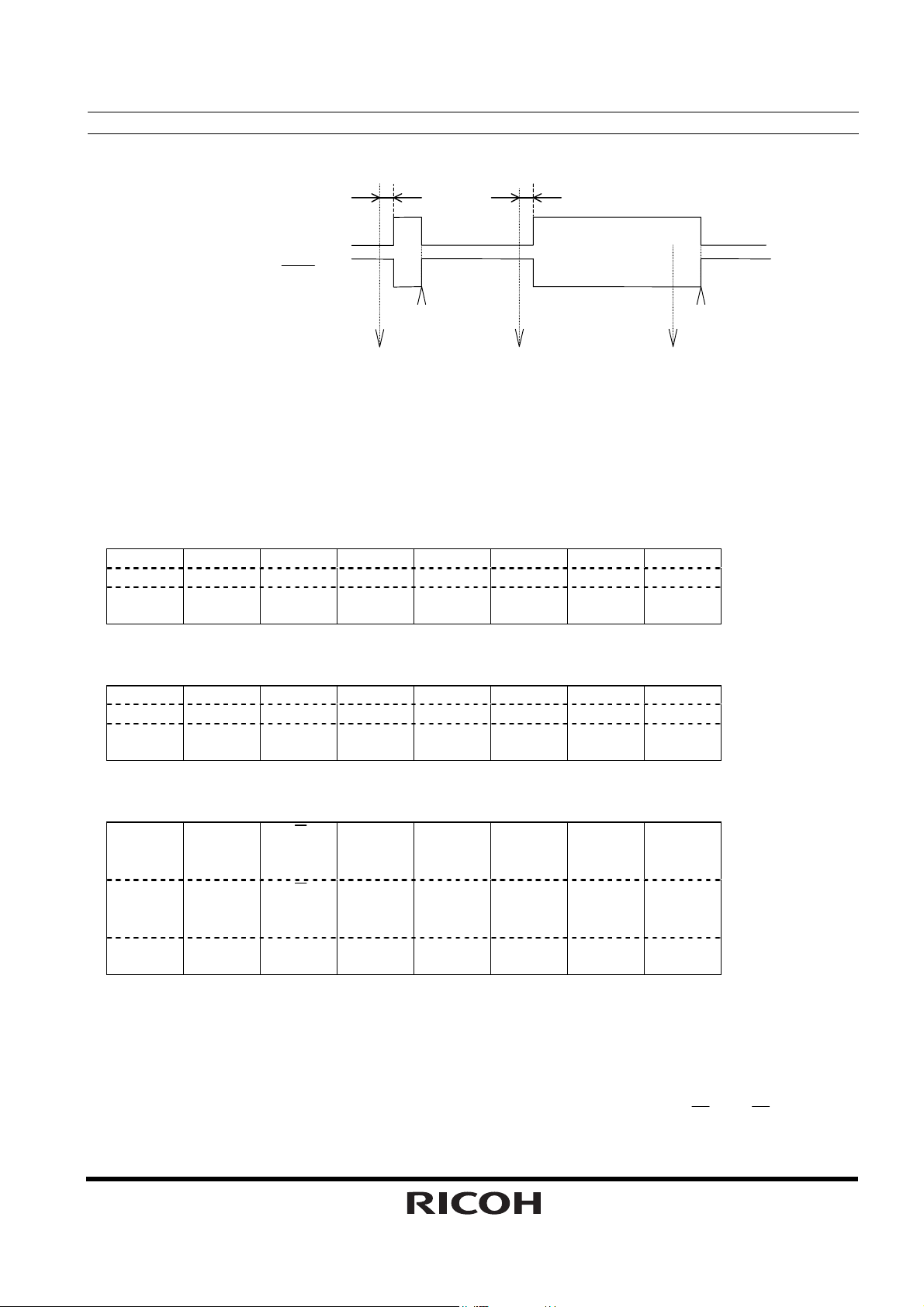
(1) Timing Between CE Pin Transition and Data Input / Output
The R2045S/D adopts a 4-wire serial interface by which they use the CE (Chip Enable), SCLK (Serial Clock),
SI (Serial Input), and SO (Serial Output) pins to receive and send data to and from the CPU. The 4-wire serial
interface provides two types of input/output timings with which the SO pin output and the SI pin input are
synchronized with the rising or falling edges of the SCLK pin input, respectively, and vice versa. The R2045S/D
is configured to select either one of two different input/output timings depending on the level of the SCLK pin in
the low to high transition of the CE pin. Namely, when the SCLK pin is held low in the low to high transition of
the CE pin, the models will select the timing with which the SO pin output is synchronized with the rising edge of
the SCLK pin input, and the SI pin input is synchronized with the falling edge of the SCLK pin in put, as illustrated
in the timing chart below.
CE
SCLK
SI
SO
t
CES
tDS
tDH
t
RD
Conversely, when the SCLK pin is held high in the low to high transition of the CE pin, the models will select
the timing with which the SO pin output is synchronized with the falling edge of the SCLK pin input, and the SI
pin input is synchronized with the rising edge of the SCLK pin input, as illustrated in the timing chart below.
CE
SCLK
SI
t
CES
t
tDH
DS
t
RD
SO
(2) Data Transfer Formats
Data transfer is commenced in the low to high transition of the CE pin input and completed in its high to low
transition. Data transfer is conducted serially in multiple units of 1 byte (8 bits). The former 4 bits are used to
specify in the Address Pointer a head address with which data transfer is to be commenced from the host. The
latter 4 bits are used to select either reading data transfer or writing dat a transfe r, and to set the Transfer Format
Register to specify an appropriate data transfer format. All data transfer formats are designed to transfer the
most significant bit (MSB) first.
21
Page 22

R2045S/D
K
r
A
A
CE
SCL
SI
A3
A1 A0 C3 C2 C1 C0
A2
6
75 8 2 312 3 1 4
D7 D6 D3 D2 D1 D0
Writing data transfer
SO
Setting
the Address Pointe
Setting the Transfer
Format Register
D7 D6 D3 D2 D1 D0
Reading data transfer
Two types of data transfer formats are available for reading data tra nsfer a nd writing data transfer each.
• Writing Data Transfer Formats
(1) 1-byte Writing Data Transfer Format
The first type of writing data transfer format is designed to transfer 1-byte data at a time and can be selected
by specifying in the address pointer a head address with which writing data transfer is to be commenced and
then writing the setting of 8h to the transfer format register. This 1-byte writing data transfer can be completed
by driving the CE pin low or continued by specifying a new head address in the address pointer and setting the
data transfer format.
Example of 1-byte Wr i t ing Data Transfer ( For Wri ting Data to Addresses Fh and 7h)
CE
SI
1 1
01 0 01 1
Data Data
0 11 0 0 01 1
SO
Specifying Fh
in the
ddress
Pointer
Setting 8h in
the Transfer
Format
Register
Data transfer from the host
Writing data to
address Fh
Specifying 7h
in the
ddress
Pointer
Setting 8h in
the Transfer
Format
Register
Data transfer from the RTCs
Writing data to
address 7h
22
Page 23

R2045S/D
A
A
A
(2) Burst Writing Data Transfer Format
The second type of writing data transfer format is designed to transfer a sequence of data serially and can be
selected by specifying in the address pointer a head address with which writing data transfer is to be
commenced and then writing the setting of 0h to the transfer format register. The address pointer is
incremented for each transfer of 1-byte data and cycled from Fh to 0h. This burst writing data transfer can be
completed by driving the CE pin low.
Example of Burst Writing Data Transfer (For Wri t ing Data to Addresses Eh, Fh, and 0h)
CE
SI
SO
1 0
Specifying Eh
in the
ddress
Pointer
00 0 01 1
Setting 0h in
the Transfer
Format
Register
Data transfer from the host Data transfer from the RTCs
Data
Writing data to
address Eh
Data
Writing data to
address Fh
Data
Writing data to
address 0h
• Reading Data Transfer Formats
(1) 1-byte Reading Data Transfer Format
The first type of reading data transfer format is designed to transfer 1-byte data at a time and can be selected
by specifying in the Address Pointer a head address with which reading data transfer is to be commenced and
then the setting of writing Ch to the Transfer Format Register. This 1-byte reading data transfer can be
completed by driving the CE pin low or continued by specifying a new head address in the Address Pointer and
selecting this type of reading data Transfer Format.
Example of 1-byte Reading Data Transfer (For Readi ng Dat a f r om Addresses Eh and 2h)
CE
SI
SO
1 0
Specifying Eh
in the
ddress
Pointer
11 0 01 1 0 10 1 0 00 1
Data Data
Setting Ch in
the Transfer
Format
Register
Reading data from
address Eh
Data transfer from the host Data transfer from the RTCs
Specifying 2h
in the
ddress
Pointer
Setting Ch in
the Transfer
Format
Register
Reading data from
address 2h
23
Page 24

R2045S/D
A
A
A
(2) Burst Reading Data Transfer Format
The second type of reading data transfer format is designed to tra nsfer a se quen ce of dat a serially and can be
selected by specifying in the address pointer a head address with which reading data transfer is to be
commenced and then writing the setting of 4h to the transfer format register. The address pointer is
incremented for each transfer of 1-byte data and cycled from Fh to 0h. This burst reading data transfer can be
completed by driving the CE pin low.
Example of Burst Reading Data Transfer (For Reading Data from Addresses Fh, 0h, and 1h)
CE
SI
SO
1 1
Specifying Fh
in the
ddress
Pointer
10 0 01 1
Setting 4h in
the Transfer
Format
Register
Data transfer from the host Data transfer from the RTCs
DATA
Reading data from
address Fh
DATA
Reading data from
address 0h
DATA
Reading data from
address 1h
(3) Combination of 1-byte Reading and writing Data Transfer Formats
The 1-byte reading and writing data transfer formats can be combined together and further followed by any
other data transfer format.
Example of Reading Modify Writing Data Transfer
(For Reading and Writing Data f rom and to Address Fh)
CE
1 1
11 0 01 1 1 11 0 0 01 1
DATASI
SO
Specifying Fh
in the
ddress
Pointer
Setting Ch in
the Transfer
Format
Register
Data transfer from the host Data transfer from the RTCs
DATA
Reading data from
address Fh
Specifying Fh
in the
ddress
Pointer
Setting 8h in
the Transfer
Format
Register
Writing data to
address Fh
24
Page 25

R2045S/D
The reading and writing data transfer formats correspond to the settings in the transfer format register as
shown in the table below.
1 Byte Burst
Writing data
transfer
Reading data
transfer
8h
(1,0,0,0)
Ch
(1,1,0,0)
0h
(0,0,0,0)
4h
(0,1,0,0)
25
Page 26

R2045S/D
• Considerations in Reading and Writing Time Data under special condition
Any carry to the second digits in the process of reading or writing time data may cause reading or writing
erroneous time data. For example, suppose a carry out of 13:59:59 into 14:00:00 occurs in the process of
reading time data in the middle of shifting from the minute digits to the hour digits. At this moment, the second
digits, the minute digits, and the hour digits read 59 seconds, 59 minutes, and 14 hours, respectively (indicating
14:59:59) to cause the reading of time data deviating from actual time virtually 1 hour. A similar error also
occurs in writing time data. To prevent such errors in reading and writing time data, the R2045S/D has the
function of temporarily locking any carry to the second digits during the high interval of the CE pin and unlocking
such a carry in its high to low transition. Note that a carry to the second digits can be locked for only 1 second,
during which time the CE pin should be driven low.
Actual time
CE
Time counts
within RTC
The effective use of this function requires the following considerations in reading and writing time data:
(1) Hold the CE pin high in each session of reading or writing time data.
(2) Ensure that the high interval of the CE pin lasts within 1 second. Should there be any possibility of the
host going down in the process of reading or writing time data, make arrangements in the peripheral circuitry as
to drive the CE pin low or open at the moment that the host actually goes down.
(3) Leave a time span of 31μs or more from the low to high transition of the CE pin to the start of access to
addresses 0h to 6h in order that any ongoing carry of the time digits may be completed within this time span.
(4) Leave a time span of 62μs or more from the high to low transition of the CE pin to its low to high transition
in order that any ongoing carry of the time digits during the high int erval of the CE pin may be adjusted within this
time span.
The considerations listed in (1), (3), and (4) above are not required when the process of re ading or writing time
data is obviously free from any carry of the time digits.
(e.g. reading or writing time data in synchronizatio n wi th the pe riodic inte rru pt fun ction in the le vel mode or t he
alarm interrupt function).
Good and bad examples of reading and writing time data are illustrated on the next page.
13:59:59 14:00:00 14:00:01
Max.62μs
13:59:59
14:00:00
14:00:01
26
Page 27

A
A
A
A
A
A
A
A
A
A
A
A
A
A
A
A
A
A
A
A
Good Example
CE
Time span of 31μs or more
ny address other than addresses 0h to 6h
permits of immediate reading or writing without
requiring a time span of 31 μs.
R2045S/D
SI
SO
F4h
ddress Pointer
= Fh
Transfer Format
Register = 4h
DATA
Reading from
ddress Fh
(control2)
DATA
Reading from
ddress 0h
(sec.)
DATA
Reading from
ddress 1h
(min.)
DATA
Reading from
ddress 2h
(hr.)
Bad Example (1)
(Where the CE pin is once driven low in the process of reading time data)
31μs or more
31μs or more
CE
SI
SO
0Ch
ddress Pointer
= 0h
Transfer Format
Register = Ch
Data
Reading from
ddress 0h
(sec.)
14h
ddress Pointer
= 1h
Transfer Format
Register = 4h
Data
Reading from
ddress 1h
(min.)
Data
Reading from
ddress 2h
(hr.)
Bad Example (2)
(Where a time span of less than 31μs is left until the start of the process of writing time data)
Time span of less than 31μs
CE
SI
F0h
Data Data Data Data
SO
Writing to
ddress 0h
(sec.)
Writing to
ddress 1h
(min.)
Writin g to
ddress 2h
(hr.)
= Fh
Transfer Format
Register = 0h
Bad Example (3)
ddress Pointer
Writin g to
ddress Fh
(contorl2)
(Where a time span of less than 61μs is left betw een the adjacent processes of reading time data)
Less than 62μs
CE
SI
SO
0Ch
0Ch
ddress Pointer
= 0h
Transfer Format
Register = Ch
Reading from
ddress 0h
(sec.)
Data transfer from the host
Data
Data
0Ch
Data
ddress Pointer
= 0h
Transfer Format
Register = Ch
Reading from
(sec.)
ddress 0h
Data transfer from RTCs
27
Page 28

R2045S/D
Correction of Time Count Deviations
• The Necessity for Correction of Time Count Deviations
The oscillation frequency for R2045S/D is corrected to 0±5ppm at 25°C in fabrication. Oscillation frequency
is the fastest at 25°C, (Please see Typical Characteristics Oscillation Frequency Deviation vs. Operating
temperature (P.
without correction of time counts deviation. Generally, a clock is corrected to gain 3 to 6ppm at 25°C.
R2045S/D is corrected it by setting clock adjustment register. Ricoh suggests to set 7Fh to clock adjustment
register (Address 7h) for time setting to gain 3ppm at 25°C, for the equipment used indoors. And suggests to
set 7Eh to clock adjustment register (Address 7h) for time setting to gain 6ppm at 25°C, for the equipment used
outdoors.
• Measurement of Oscillation Frequency
42)). In normal condition, temperature is not kept constant at 25°C. That is, R2045S/D loses
VDD
Frequency
Counter
VSS
32KOUT
* 1) When power-on, the R2045S/D is configured to generate 32.768-kHz clock pulses for output from the
32KOUT pin.
* 2) A frequency counter with 6 (more preferably 7) or more digits on the ord er of 1ppm is recommended for
use in the measurement of the oscillation frequency of the oscillation circuit.
• Oscillation Adjustment Circuit
The oscillation adjustment circuit can be used to correct a time count gain or loss with high precision by
varying the number of 1-second clock pulses once per 20 seconds. The oscillation adjustment circuit can be
disabled by writing the settings of "*, 0, 0, 0, 0, 0, *" ("*" representing "0" or "1") to the F6, F5, F4, F3, F2, F1, and
F0 bits in the oscillation adjustment circuit. Conversely, when such oscillation adjustment is to be made, an
appropriate oscillation adjustment value can be calculated by the equation below for writing to the oscillation
adjustment circuit.
(1) When Oscillation Frequency (* 1) Is Higher Than Target Frequency (* 2) (Causing Time Count Gain)
Oscillation adjustment value (*3) = (Oscillation frequency - Target Frequency + 0.1)
Oscillation frequency × 3.051 × 10
≈ (Oscillation Frequency – Target Frequency) × 10 + 1
-6
28
Page 29

R2045S/D
* 1) Oscillation frequency:
Frequency of clock pulse output from the 32KOUT pin at normal temperature in the manner described in "
P
28 • Measurement of Oscillation Frequency".
* 2) Target frequency:
Desired frequency to be set. Generally, a 32.768-kHz crystal oscillator has such temperature
characteristics as to have the highest oscillation frequency at normal temperature. Consequently, the
crystal oscillator is recommended to have target frequency settings on the order of 32.768 to 32.76810 kHz
(+3.05ppm relative to 32.768 kHz). Note that the target frequency differs depending on the environment
or location where the equipment incorporating the RTC is expected to be operated.
* 3) Oscillation adjustment value:
Value that is to be finally written to the F0 to F6 bits in the Oscillation Adjustment Register and is
represented in 7-bit coded decimal notation.
(2) When Oscillation Frequency Is Equal To Target Frequency (Causing Time Count neither Gain nor Loss)
Oscillation adjustment value = 0, +1, -64, or –63
(3) When Oscillation Frequency Is Lower Than Target Frequency (Causing Time Count Loss)
Oscillation adjustment value = (Oscillation frequency - Target Frequency)
Oscillation frequency × 3.051 × 10
≈ (Oscillation Frequency – Target Frequency) × 10
Oscillation adjustment value calculations are exemplified below
(A) For an oscillation frequency = 32768.85Hz and a target frequency = 32768.05Hz
Oscillation adjustment value = (32768.85 - 32768.05 + 0.1) / (32768.85 × 3.051 × 10
≈ (32768.85 - 32768.05) × 10 + 1
= 9.001 ≈ 9
In this instance, write the settings ((0),F6,F5,F4,F3,F2,F1,F0)=(0,0,0,0,1,0,0,1) in the oscillation adjustment
register. Thus, an appropriate oscillation adjustment value in the presence of any time count gain represents a
distance from 01h.
(B) For an oscillation frequency = 32762.22Hz and a target frequency = 32768.05Hz
Oscillation adjustment value = (32762.22 - 32768.05) / (32762.22 × 3.051 × 10
≈ (32762.22 - 32768.05) × 10
= -58.325 ≈ -58
To represent an oscillation adjustment value of - 58 in 7-bit coded decimal notation, subtract 58 (3Ah) from 128
(80h) to obtain 46h. In this instance, write the settings of ((0),F6,F5,F4,F3,F2,F1,F0) = (0,1,0,0,0,1,1,0) in the
oscillation adjustment register. Thus, an appropriate oscillation adjustment value in the presence of any time
count loss represents a distance from 80h.
Notes:
1) Oscillation adjustment does not affect the frequency of 32.768-kHz clock pulses output from the
32KOUT pin.
2) Oscillation adjustment value range: When the oscillation frequency is higher than the target frequency
(causing a time count gain), an appropriate time count gain ranges from -3.05ppm to -189.2ppm with the
settings of "0, 0, 0, 0, 0, 1, 0" to "0, 1, 1, 1, 1, 1, 1" written to the F6, F5, F4, F3, F2, F1, and F0 bits in the
oscillation adjustment register, thus allowing correction of a time count gain of up to +189.2ppm.
-6
-6
)
-6
)
29
Page 30

R2045S/D
Conversely, when the oscillation frequency is lower than the target frequency (causing a time count loss),
an appropriate time count gain ranges from +3.05ppm to +189.2ppm with the settings of "1, 1, 1, 1, 1, 1, 1"
to "1, 0, 0, 0, 0, 1, 0" written to the F6, F5, F4, F3, F2, F1, and F0 bits in the oscillation adjustment register,
thus allowing correction of a time count loss of up to -189.2ppm.
3) If following 3 conditions are completed, actual clock adjustment value could be different from target
adjustment value that set by oscillator adjustment function.
1. Using oscillator adjustment function
2. Access to R2045S/D at random, or synchronized with external clock that has no relation to R20 45S/D, or
synchronized with periodic interrupt in pulse mode.
3. Access to R2045S/D more than 2 times per each second on average.
For more details, please contact to Ricoh.
• How to evaluate the clock gain or loss
The oscillator adjustment circuit is configured to change time count s of 1 seco nd on the basi s of the settings of
the oscillation adjustment register once in 20 seconds. The oscillation adjustment circuit does not effect the
frequency of 32768Hz-clock pulse output from the 32OUT pin. Therefore, after writing the oscillation
adjustment register, we can not measure the clo ck error with probi ng 32KOUT clock pulses. The way t o meas ure
the clock error as follows:
(1) Output a 1Hz clock pulse of Pulse Mode with interrupt pin
Set (0,0,x,x,0,0,1,1) to Control Register 1 at address Eh.
(2) After setting the oscillation adjustment register, 1Hz clock period changes every 20seconds ( or every 60
seconds) like next page figure.
1Hz clock pulse
T0 T0 T0 T1
1 time19 times
Measure the interval of T0 and T1 with frequency counter. A frequency counter with 7 or more digits is
recommended for the measurement.
(3) Calculate the typical period from T0 and T1
T = (19×T0+1×T1)/20
Calculate the time error from T.
30
Page 31

X
Power-on Reset, Oscillation Halt Sensing, and Supply Voltage
Monitoring
R2045S/D
• PON,
The power-on reset circuit is configured to reset control register1, 2, and clock adjustment register when VDD
power up from 0v. The oscillation halt sensing circuit is configured to record a halt on oscillation by 32.768-kHz
clock pulses. The supply voltage monitoring circuit is configured to record a drop in supply voltage below a
threshold voltage of 2.1 or 1.3v.
Each function has a monitor bit. I.e. the PON bit is for the power-on reset circuit, and
oscillation halt sensing circuit, and VDET is for the supply voltage monitoring circuit. PON and VDET bits are
activated to “H”. However,
XST
0, and
The functions of these three monitor bits are shown in the table below.
The relationship between the PON,
XST
, and VDET
XST
bit is for the
XST
bit is activated to “L”. The PON and VDET accept only the writing of 0, but
accepts the writing of 0 and 1. The PON bit is set to 1, when VDD power-up from 0V, but VDET is set to
XST
is indefinite.
PON
Function Monitoring for the
power-on reset function
Address D4 in Address Fh D5 in Address Fh D6 in Address Fh
Activated High Low High
When VDD power
up from 0v
accept the writing 0 only Both 0 and 1 0 only
PON
0 0 0 Halt on oscillation, but no drop in
0 0 1 Halt on oscillation and drop in VDD
0 1 0 No drop in VDD supply voltage
0 1 1 Drop in VDD supply voltage below
1 * * Drop in supply voltage to 0v Power-up from 0v,
XST
1 indefinite 0
XST
, and VDET is shown in the table below.
VDET Conditions of supply voltage
and oscillation
VDD supply voltage below
threshold voltage
supply voltage below threshold
voltage, but no drop to 0V
below threshold voltage and no
halt in oscillation
threshold voltage and no halt on
oscillation
Monitoring for the
oscillation halt sensing
function
ST
a drop in supply voltage
below a threshold voltage
of 2.1 or 1.3v
Condition of oscillator, and
back-up status
Halt on oscillation cause of
condensation etc.
Halt on oscillation cause of drop in
back-up battery voltage
Normal condition
No halt on oscillation, but drop in
back-up battery voltage
VDET
31
Page 32

R2045S/D
g
(
)
32768Hz Oscillation
Power-on reset flag
Oscillation halt
sensin
VDD supply voltage
monitor flag (VDET)
flag
VDD
(PON)
XST
Threshold voltage (2.1V or 1.3V)
Internal initialization
period (1 to 2 sec.)
VDET←0
XST
←1
PON←0
VDET←0
XST
←1
PON←1
Internal initialization
period (1 to 2 sec.)
VDET←0
XST
←1
PON←0
When the PON bit is set to 1 in the control register 2, the DEV, F6 to F0, WALE, DALE,
TEST, CT2, CT1, CT0, VDSL, VDET,
CLEN1
, CTFG, WAFG, and DAFG bits are reset to 0 in the oscillation
12
/24,
CLEN2
adjustment register , the control register 1, and the control re gister 2. The PON bit is also set to 1 at power-on
from 0 volts.
< Considerations in Using Oscillation Halt Sensing Circuit >
Be sure to prevent the oscillation halt sensing circuit from malfunctioning by preventing the following:
1) Instantaneous power-down on the VDD
2) Applying to individual pins voltage exceeding their respective maximum ratings
XST
In particular, note that the
bit may fail to be set to 0 in the presence of any applied supply voltage as
illustrated below in such events as backup battery installation. Further, give special considerations to prevent
excessive chattering in the oscillation halt sensing circuit.
VDD
,
32
Page 33

R2045S/D
(
)
(
)
• Voltage Monitoring Circuit
The VDD supply voltage monitoring circuit is configured to conduct a sampling operation during an interval of
7.8ms per second to check for a drop in supply voltage below a threshold voltage of 2.1 or 1.3v for the VDSL bit
setting of 0 (the default setting) or 1, respectively, in the Control Register 2, thus minimizing supply current
requirements as illustrated in the timing chart below. This circuit suspends a sampling operation once the
VDET bit is set to 1 in the Control Register 2. The VDD supply voltage monitor is useful for back-up battery
checking.
Sampling timing for
VDD supply voltage
D6 in Address Fh
VDD
PON
VDET
Internal
nitiali-zation
period
1 to 2sec.
PON←0
←0
VDET
2.1v or 1.3v
7.8ms
1s
VDET←0
33
Page 34

R2045S/D
Alarm and Periodic Interrupt
The R2045S/D incorporates the alarm interrupt circuit and the periodic interrupt circuit that are configured to
generate alarm signals and periodic interrupt signals, respectively, for output from the
below.
(1) Alarm Interru pt Cir cuit
The alarm interrupt circuit is configured to generate alarm signals for output from the
low (enabled) upon the occurrence of a match between current time read by the time counters (the day-of-week,
hour, and minute cou nters) and alarm time preset by the alarm registers (the Alarm_W registers intended for the
day-of-week, hour, and minute digit settings and the Alarm_D registers intended for the hour and minute digit
settings). Both The Alarm_W and Alarm_D are output from the
(2) Periodic Interrupt Circuit
The periodic interrupt circuit is configured to generate either clock pulse s in the pulse mode or interrupt signals
in the level mode for output from the
register 1.
The above two types of interrupt signals are monitored by the flag bits (i.e. the WAFG, DAFG, and CTFG bits in
the Control Register 2) and enabled or disabled by the enable bits (i.e. the WALE, DALE, CT2, CT1, and CT0
bits in the Control Register 1) as listed in the table below.
Flag bits Enable bits
Alarm_W WAFG
(D1 at Address Fh)
Alarm_D DAFG
(D0 at Address Fh)
Peridic
Interrupt
* At power-on, when the WALE, DALE, CT2, CT1, and CT0 bits are set to 0 in the Control Register 1, the
INTR
pin is driven high (disabled).
* When two types of interrupt signals are output simultaneously from the
INTR
pin becomes an OR waveform of their negative logic.
CTFG
(D2 at Address Fh)
Example: Combined Output to
INTR
pin depending on the CT2, CT1, and CT0 bit settings in the control
WALE
(D7 at Address Eh)
DALE
(D6 at Address Eh)
CT2=CT1=CT0=0
(These bit setting of “0” disable the Periodic Interrupt)
(D2 to D0 at Address Eh)
INTR
Alarm_D and Periodic Interrupt
INTR
.
INTR
Pin Under Control of
INTR
pin as described
INTR
, which is driven
pin, the output from the
34
Alarm_D
Periodic Interrupt
IN T R
In this event, which type of interrupt signal is output from the
DAFG, and CTFG bit settings in the Control Register 2.
INTR
pin can be confirmed by reading the
Page 35

R2045S/D
←
• Alarm Interrupt
The alarm interrupt circuit is controlled by the enable bits (i.e. the WALE and DALE bits in the Control Register
1) and the flag bits (i.e. the WAFG and DAFG bits in the Control Register 2). The enable bits can be used to
enable this circuit when set to 1 and to disable it when set to 0. When intended for reading, the flag bits can be
used to monitor alarm interrupt signals. When intended for writing, the flag bits will cause no event when set to
1 and will drive high (disable) the alarm interrupt circuit when set to 0.
The enable bits will not be affected even when the flag bits are set to 0. In this event, therefore, the alarm
interrupt circuit will continue to function until it is driven low (enabled) upon the next occurrence of a match
between current time and preset alarm time.
The alarm function can be set by presetting desired alarm time in the alarm registers (the Alarm_W Registers
for the day-of-week digit settings and both the Alarm_W Registers and the Alarm_D Registers for the hour and
minute digit settings) with the WALE and DALE bits once set to 0 and then to 1 in the Control Register 1. Note
that the WALE and DALE bits should be once set to 0 in order to disable the alarm interrupt circuit upon the
coincidental occurrence of a match between current time and preset alarm time in the process of setting the
alarm function.
Interval (1min.) during which a match
between current time and preset alarm time
occurs
INTR
INTR
WALE←1
(DALE)
WALE←1
(DALE)
current time =
preset alarm time
current time =
preset alarm time
WALE
(DALE)
WALE←1
0
(DALE)
WAFG←0
(DAFG)
current time =
preset alarm time
current time =
preset alarm time
35
Page 36

R2045S/D
A
• Periodic Interrupt
Setting of the periodic selection bits (CT2 to CT0) enables periodic interrupt to the CPU. There are two
waveform modes: pulse mode and level mode. In the pulse mode, the output has a waveform duty cycle of
around 50%. In the level mode, the output is cyclically driven low and, whe n the CTFG bit is set to 0, the outp ut is
return to High (OFF).
CT2 CT1 CT0
Wave form
mode
0 0 0 - OFF(H) (Default)
0 0 1 - Fixed at “L”
0 1 0 Pulse Mode *1) 2Hz(Duty50%)
0 1 1 Pulse Mode *1) 1Hz(Duty50%)
1 0 0 Level Mode *2) Once per 1 second (Synchronized with
1 0 1 Level Mode *2) Once per 1 minute (at 00 seconds of every
1 1 0 Level Mode *2) Once per hour (at 00 minutes and 00
1 1 1 Level Mode *2) Once per month (at 00 hours, 00 minutes,
*1) Pulse Mode: 2-Hz and 1-Hz clock pulses are output in synch ronization with the increm ent of the second
counter as illustrated in the timing chart below.
Description
Interrupt Cycle and Falling Timing
Second counter increment)
Minute)
Seconds of every hour)
and 00 seconds of first day of every month)
In the pulse mode, the increment of the second counter is delayed by approximately 92 μs from the falling
edge of clock pulses. Consequently, time readings immediately after the falling edge of clock pulses may
appear to lag behind the time counts of the real-time clocks by approximately 1 second. Rewriting the
second counter will reset the other time counters of less than 1 second, driving the
*2) Level Mode: Periodic interrupt signals are output with selectable interrupt cycle settings of 1 second, 1
minute, 1 hour, and 1 month. The increment of the second counter is synchronized with the falling edge of
periodic interrupt signals. For example, periodic interrupt signals with an interrupt cycle setting of 1
second are output in synchronization with the increment of the second counter as illustrated in the timing
chart below.
CTFG Bit
INTR Pin
pprox. 92μs
(Increment of second counter)
INTR
pin low.
Rewriting of the second counter
36
Page 37

R2045S/D
*1), *2) When the oscillation adjustment circuit is used, the interrupt cycle will fluctuate once per 20sec. as
follows:
Pulse Mode:
The “L” period of output pulses will increment or decrement by a maximum of ±3.784ms. For example, 1-Hz
clock pulses will have a duty cycle of 50 ±0.3784%.
Level Mode:
A periodic interrupt cycle of 1 second will increment or decrement by a maximum of ±3.784 ms.
CTFG Bit
INTR Pin
Setting CTFG bit to 0
(Increment of
second counter)
(Increment of
second counter)
Setting CTFG bit to 0
(Increment of
second counter)
32-kHz CLOCK OUTPUT
For the R2045S/D, 32.768-kHz clock pulses are output from the 32KOUT pin when
is set to Low. If
The 32KOUT pin output is synchronized with the
timing chart below.
CLEN1
CLEN1
(D3 at Address Fh)
1 1 OFF(H)
0(Default) *
* 0(Default)
and
bit
CLEN2
are set to high, the 32KOUT pin is high impedance.
CLEN2
(D4 at Address Eh)
bit
CLEN1
32KOUT output pin
(N-channel open
drain output)
32kHz clock output
CLEN2
and
bit settings as illustrated in the
CLEN1
or
CLEN2
bit
CLEN1or2
32KOUT PIN
Max.62.0μs
Max.45.8μs
37
Page 38

R2045S/D
t
Typical Applications
• Typical Power Circuit Configurations
Sample circuit configuration 1
System power supply
VDD
*1)
VSS
Sample circuit configuration 2
System power supply
VDD
*1)
Primary
VSS
Battery
System power supply
*1) Install bypass capacitors for high frequency and
low frequency applications in parallel in close
vicinity to the R2045S/D.
*1) When using an OR diode as a power supply for the
R2045S/D ensure that voltage exceeding the
absolute maximum rating of VDD+0.3v is no
applied the SO pin.
38
VDD
*1)
Secondary
VSS
Battery
Page 39

R2045S/D
A
A
t
• Connection of
INTR
The
supply side. As such, it can be connected to a pull-up resistor of up to 5.5 volts regardless of supply voltage.
INTR
Pin
pin follows the N-channel open drain output logic and contains no protective diode on the power
INTR
VDD
VSS
System power supply
*1)
B
Backup power supply
*1) Depending on whether the
be used during battery backup, it should be
connected to a pull-up resistor at the following
different positions:
(1) Position A in the left diagram when it is not to
be used during battery backup.
(2) Position B in the left diagram when it is to be
used during battery backup.
INTR
pin is to
• Connection of 32KOUT Pin
The 32KOUT pin follows the Nch. open drain output and contains no protective diode on the power supply
side. As such, it can be connected to a device with a supply voltage of up to 5.5 volts regardless of supply
voltage, provided that such connection involves considerations for the supply current requirements of a pull-up
resistor, which can be roughly calculated by the following equation:
I = 0.5 × (V
32KOUT
VDD
VSS
DD or VCC) / Rp
System power supply
B
Backup power supply
*1)
*1) Depending on whether the 32KOUT pin is
to be used during battery backup, it should
be connected to a pull-up resistor at the
following different positions:
(1) Position A in the left diagram when it is no
to be used during battery backup.
(2) Position B in the left diagram when it is to
be used during battery backup.
39
Page 40

R2045S/D
K
A
• Connection of CE Pin
Connection of the CE pin requires the following considerations:
1) The CE pin is configured to enable the oscillation halt sensing circuit only when driven low. As such, it
should be driven low or open at power-on from 0 volts.
2) The CE pin should also be driven low or open immediately upon the host going down (see P.
"
Considerations in Reading and Writing Time Data under special condition").
SCLK
26
I/O
CONTROL
SI
SO
CE
VDD
CE
Min.0μsMin.0μs
Lower limit operating
voltage for the CPU
Backup power supply
0.2×VDD
Min.0μs
• Connection With 3-Wire Serial Interface Bus
To connect the R2045S/D with 3-wire serial interface bus, shorten the SI and SO pins and connect them to the
data line as shown in the figure below.
Host
CE0
CE1
SCL
DAT
CE
SCLK
R2045S/D
SI
SO
40
CE
SCLK
SIO
The other
Peripheral IC
Page 41

Typical Characteristics
Test Circuit
R2045S/D
VDD
Topt : 25°C
Output : Open
CL
Frequency
Counter
32KOUT
VSS
Timekeeping current vs. Supply Voltage Timekeeping current vs. Supply Voltage
(with no 32-kHz clock output) (witj 32-kHz clock output)
(Output=Open, Topt=25°C) (Output=Open, Topt=25°C)
1.2
1
0.8
0.6
0.4
0.2
1.2
1
0.8
0.6
0.4
0.2
0
Timekeeping current IDD(uA)
0123456
Supply Voltage VDD(v)
0
Timekeeping current IDD(uA)
0123456
Supply Voltage VDD(v)
CPU Access Current vs. SCL Clock Frequency Timekeeping current vs. Operating
Temperature
(Output=Open, Topt=25°C) (Output=Open, V
DD=3V)
(wiithout pull-up resister current)
40
1
32KOUT output
30
20
10
CPU Access Current IDD(uA)
V
=5v
DD
V
DD
0
0 200 400 600 800 1000
SCL Clock Frequency (kHz)
=3v
0.8
0.6
0.4
0.2
0
Timekeeping Current IDD(uA)
-60 -40 -20 0 20 40 60 80 100
no 32KOUT output
Operating Temperature Topt(Celsius)
41
Page 42

R2045S/D
Oscillation Frequency Deviation vs. Supply Voltage Oscillation Frequency Deviation vs.
(Topt=25°C) Operating Temperature
(V
DD=3v)
5
4
3
2
1
0
-1
-2
Deviation (ppm)
-3
-4
Oscillation Frequency
-5
0123456
Power Supply VDD (v)
Oscillation frequency
V
OL vs. IOL(
INTR
pin) VOL vs. IOL(
(Topt=25°C) (V
35
30
25
20
15
IOL (mA)
10
5
0
00.20.40.60.81
V
DD
VOL (v)
=5v
V
DD
=3v
35
30
25
20
15
IOL (mA)
10
5
0
Oscillation Start Time vs. Power Supply
(Topt=25°C)
20
0
-20
-40
-60
-80
Deviation (ppm)
-100
-120
-60 -40 -20 0 20 40 60 80 100
Operat i ng Temperature Topt(Cel sius)
INTR
pin)
IN=VDD,Topt=25°C)
00.20.40.60.81
VOL (v)
42
500
400
300
200
100
Oscillation Start Time (ms)
0
0123456
Power Supply VDD (v)
Page 43

Typical Software-based Operations
• Initialization at Power-on
Start
*1)
Power-on
R2045S/D
*2)
PON=1?
Yes
Set
Contr ol Register 1 and 2,
etc.
*1) After power-on from 0 volt, the start of oscillation and the process of internal initialization require a time
span on the order of 1 to 2sec, so that access should be done after the lapse of this time span or more.
*2) The PON bit setting of 0 in the Control Register 1 indicates power-on from backup battery and not from
0v. For further details, see "P.
Monitoring • PON,
*3) This step is not required when the supply voltage monitoring circuit is not used.
*4) This step involves ordinary initialization including the Oscillation Adjustment Register and i nterrupt cycle
settings, etc.
*4)
XST
No
*3)
VDET=0?
Yes
31 Power-on Reset, Oscillation Halt Sensing, and Supply Voltage
, and VDET ".
No
Warning Back-up
Battery Run-down
43
Page 44

R2045S/D
• Writing of Time and Calendar Data
*1) When writing to clock and calendar counters , do not drive CE to L until
all times from second to year have been written to prevent error in
writing time. For more detailed in "P.25 Considerations in Reading
and Writing Time Data under special condition".
*2) Any writing to the second counter will reset divider units lower than the
second digits.
*3) Please see “P,27 The Necessity for Correction of Time Count
Deviations”
The R2045S/D may also be initialized not at power-on but in the
process of writing time and calendar data.
CE ← H
Write to Time Counter and
Calendar Counter
Write to Clock Adjustment
Register
CE←L
*1)
*2)
*3)
*1)
• Reading Time and Calendar Data
(1) Ordinary Process of Reading Time and Calendar Data
CE ← H
Read from Time Counter
and Calendar Counter
*1)
*1) When reading clock and calendar counters, do not drive CE t o L until
all times from second to year have been written to prevent error in
writing time. For more detailed in "P.25 Considerations in Reading
and Writing Time Data under special condition".
44
CE ← L
*1)
Page 45

(2) Basic Process of Reading Time and Calendar Data with Periodic Interrupt Fu nction
R2045S/D
Set Periodic Interrupt
Cycle Selection Bits
Generate Interrupt in CPU
CTFG=1?
Yes
Read from Time Counter
and Calendar Counter
Contr o l Register 2
(X1X1X011)
←
*2)
*3)
*1)
No
Other Interrupt
Processes
*1) This step is intended to select the level mode as a
waveform mode for the periodic interrupt function.
*2) This step must be completed within 1.0 second.
*3) This step is intended to set the CTFG bit to 0 in the
Control Register 2 to cancel an interrupt to the CPU.
45
Page 46

R2045S/D
r
(3) Applied Proces s of Reading Time and Cale ndar Data with Periodic Interrupt Function
Time data need not be read from all the time counters when used for such ordinary purposes as time count
indication. This applied process can be used to read time and calendar data with substantial reductions in
the load involved in such reading.
For Time Indi cation in "Day-of-Month, Day-of-week, Hour, Minute, and Seco nd" Format:
Control Register 1
(XXXX0100)
Control Register 2
(X1X1X011)
Generate interrupt to CPU
CTFG=1?
Yes
Sec.=00?
Yes
Read M in.,Hr.,Day,
and Day-of - week
Contr o l Register 2
(X1X1X011)
←
←
*2)
←
*1)
No
No
*3)
Use Prev ious Min.,Hr.,
Day,and Day-of-w eek data
*4)
Other interrupts
Processes
*1) This step is intended to select the
level mode as a waveform mode fo
the periodic interrupt function.
*2) This step must be completed within
1.0 sec.
*3) This step is intended to read time
data from all the time counters only in
the first session of reading time data
after writing time data.
*4) This step is intended to set the CTFG
bit to 0 in the Control Register 2 to
cancel an interrupt to the CPU.
46
Page 47

• Interrupt Process
(1) Periodic Interrupt
R2045S/D
Set Periodic Interrupt
Cycle Selection Bits
Generate Interrupt to CPU
CTFG=1?
Yes
Conduct
Periodic Interrupt
Contr o l Register 2
(X1X1X011)
←
*2)
*1)
No
*1) This step is intended to select the level mode as a
waveform mode for the periodic interrupt function.
*2) This step is intended to set the CTFG bit to 0 in
the Control Register 2 to cancel an interrupt to the
CPU.
Other Interrupt
Processes
47
Page 48

R2045S/D
t
(2) Alarm Interrupt
WALE or DALE←0
Set Alarm Min., Hr., and
Day-of-we ek Register s
WALE or DALE←1
Generate Interrupt to CPU
WAFG or DAFG=1?
Yes
Conduct Alarm Interr upt
Control Register 2
(X1X1X101)
←
*3)
*1)
*2)
No
Other Interrupt
*1) This step is intended to once disable the alarm
interrupt circuit by setting the WALE or DALE bits to 0
in anticipation of the coincidental occurrence of a
match between current time and preset alarm time in
the process of setting the alarm interrupt function.
*2) This step is intended to enable the alarm interrup
function after completion of all alarm interrupt settings.
*3) This step is intended to once cancel the alarm
interrupt function by writing the settings of "X,1,X,
1,X,1,0,1" and "X,1,X,1,X,1,1,0" to the Alarm_W
Registers and the Alarm_D Registers, respectively.
Processes
48
Page 49

y
Land Pattern (reference)
• R2045S (SOP14)
R2045S/D
14
5.4 1.4 1.4
1
0.7
P 1.27x6=7.62
8.32
8
7
1.27
unit:mm
Package top view
14
8
1
7
1. Pad layout and size can modify by customers material, equipment, and method. Please adjust pad layout
according to your conditions.
2. In the mount area which desc ried as , is close to the inside oscillator circuit. T o avoid the malfunction b
noise, check the other signal lines close to the area, do not intervene with the oscillator circuit.
3. A part of a metal case of the crystal may be seen in the area which described as in both sides of the
package. It has no influence on the characteristics and quality of the product.
49
Page 50

R2045S/D
• R2045D (SON22)
22
4.0 0.7 0.7
0.8
1 11
0.7
Package top view Package bottom view
22 14
P 0.5x10=5.0
0.25 0.75
14
0.25
0.5
14
1.4
0.8
0.75.25
unit : mm
22
50
1 11
11
1
1. Pad layout and size can modify by customers material, equipm ent, and m ethod. Please adj ust pad layout
according to your conditions.
2. Any signal line should not pass through the area that described as in the land pattern. If a signal
line is located in that area, it may cause a short circuit with a tab suspension leads which is marked with
in the figure above or unnecessary remainder of cut lead.
3. In the mount area which descried as , is close to the inside oscillator circuit. To avoid the m alf unction
by noise, check the other signal lines close to the area, do not intervene with the oscillator circuit.
4. A part of a metal case of the crystal may be seen in the area that described as in both sides of the
package. It has no influence on the characteristics and quality of the product.
Page 51

RICOHCOMPANY,LTD.
ElectronicDevicesCompany
●Shin-Yokohamaoffice(InternationalSales)
3-2-3,Shin-Yokohama,Kohoku-ku,YokohamaCity,Kanagawa222-8530,Japan
Phone:+81-45-477-1697Fax:+81-45-477-1698
RICOHEUROPE(NETHERLANDS)B.V.
●SemiconductorSupportCentre
Prof.W.H.Keesomlaan1,1183DLAmstelveen,TheNetherlands
P.O.Box114,1180ACAmstelveen
Phone:+31-20-5474-309Fax:+31-20-5474-791
RICOHELECTRONICDEVICESKOREACo.,Ltd.
11floor,Haesung1building,942,Daechidong,Gangnamgu,Seoul,Korea
Phone:+82-2-2135-5700Fax:+82-2-2135-5705
RICOHELECTRONICDEVICESSHANGHAICo.,Ltd.
Room403,No.2Building,690#BiBoRoad,PuDongNewdistrict,Shanghai201203,
People'sRepublicofChina
Phone:+86-21-5027-3200Fax:+86-21-5027-3299
RICOHCOMPANY,LTD.
ElectronicDevicesCompany
●Taipeioffice
Room109,10F-1,No.51,HengyangRd.,TaipeiCity,Taiwan(R.O.C.)
Phone:+886-2-2313-1621/1622Fax:+886-2-2313-1623
http://www.ricoh.com/LSI/
1.Theproductsandtheproductspecificationsdescribedinthisdocumentaresubjecttochangeor
discontinuationofproductionwithoutnoticeforreasons
suchasimprovement.Therefore,before
decidingtousetheproducts,pleaserefertoRicohsalesrepresentativesforthelatest
informationthereon.
2.Thematerialsinthisdocumentmaynotbecopiedorotherwisereproducedinwholeorinpart
withoutpriorwrittenconsentofRicoh.
3.Pleasebesuretotakeanynecessaryformalitiesunderrelevantlawsorregulationsbefore
exportingorotherwisetakingoutofyourcountrytheproductsorthetechnicalinformation
describedherein.
4.Thetechnicalinformationdescribedinthisdocumentshowstypicalcharacteristicsofand
exampleapplicationcircuitsfortheproducts.Thereleaseofsuchinformationisnottobe
construedasawarrantyoforagrantoflicenseunderRicoh'soranythirdparty'sintellectual
propertyrightsoranyotherrights.
5.
Theproductslistedinthisdocumentareintendedanddesignedforuseasgeneralelectronic
componentsinstandardapplications(officeequipment,telecommunicationequipment,
measuringinstruments,consumerelectronicproducts,amusementequipmentetc.).Those
customersintendingtouse
aproductinanapplicationrequiringextremequalityandreliability,
forexample,inahighlyspecificapplicationwherethefailureormisoperationoftheproduct
couldresultinhumaninjuryordeath(aircraft,spacevehicle,nuclearreactorcontrolsystem,
trafficcontrolsystem,automotiveand
transportationequipment,combustionequipment,safety
devices,lifesupportsystemetc.)shouldfirstcontactus.
6.Wearemakingourcontinuousefforttoimprovethequalityandreliabilityofourproducts,but
semiconductorproductsarelikelytofailwithcertainprobability.Inordertopreventanyinjuryto
personsordamagestopropertyresultingfromsuchfailure,customersshouldbecarefulenough
toincorporatesafetymeasuresintheirdesign,suchasredundancyfeature,firecontainment
featureandfail-safefeature.Wedonotassumeanyliability
orresponsibilityforanylossor
damagearisingfrommisuseorinappropriateuseoftheproducts.
7.Anti-radiationdesignisnotimplementedintheproductsdescribedinthisdocument.
8.
PleasecontactRicohsalesrepresentativesshouldyouhaveanyquestionsorcomments
concerningtheproductsorthetechnicalinformation.
RICOHCOMPANY.,LTD.ElectronicDevicesCompany
■
Ricoh presen ted with th e Japa n Management Qual ity Awa rd for 1 999
.
Ricoh con tinually s trives to promote c ustomer s atisfaction , and sha res the a chievements
of its ma nagement quality im provement program with people a nd societ y.
■R ic o h aw ard ed I SO 1 4001 cert ifi ca tion .
The Ricoh Group was awa rded ISO 1 4001 cer tification, which is an interna tional standard for
environm ental manage ment systems, at both its d omestic and overseas production facilities.
Our cur rent ai m is to obtain ISO 14 001 certific ation for all o f our busine ss office s.
Ricoh com pleted th e organiza tion of the Lead-f ree produ ction for a ll of our products.
After Apr. 1, 200 6, we will ship out the lead free pro ducts onl y. Thus, all products that
will be shipped from now on comply with RoHS Directive.
 Loading...