

Page 1
R192P OC-192/STM-64 Lightwave Receiver
with Improved Sensitivity (–18 dBm)
Features
■
High data rate capability, 10.7 Gbits/s
■
PIN photodetector
■
Fully operational through the 1.3 µm to 1.6 µm
wavelength range
■
Improved typical sensitivity of –18 dBm
■
Single-mode fiber pigtail with
FC/PC optical connector
Preliminary Data Sheet, Rev. 4
June 2001
®
ST
, SC, LC, or
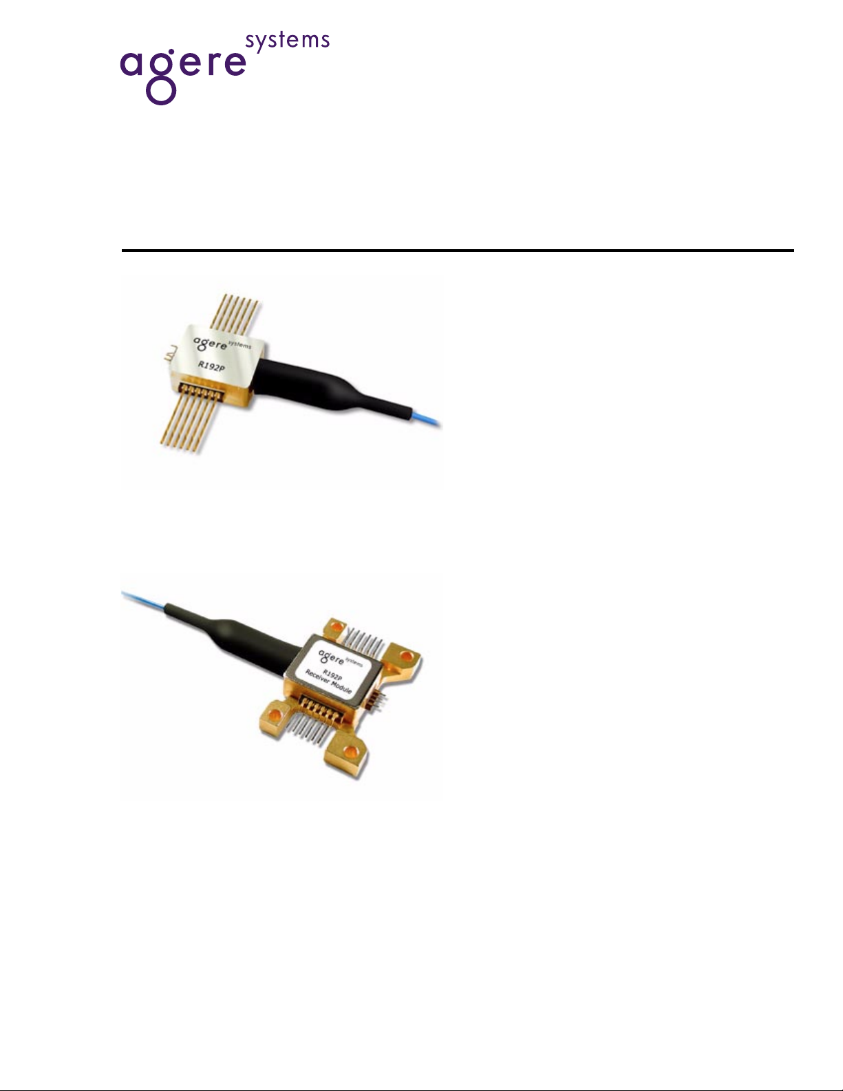
Featuring improved sensitivity for optimum performance in
noisy, amplified systems, the R192P Receiver is manufactured in a compact, 16-pin surface-mount package (above),
and is also available with a convenient mounting bracket
(below).
■
Operating case temperature range:
0 °C to 70 °C
■
50 Ω differential data output, with offset control
■
Package options:
— Space-sensitive package without mounting
bracket (ideal for transponder and transceiver
applications)
— With mounting bracket
Applications
■
Line terminal equipment
■
High-speed networks up to 10.7 Gbits/s
■
SONET/SDH OC-192/STM-64 telecommunications applications
■
Extended-reach datacom and telecom applications
Page 2

R192P OC-192/STM-64 Lightwave Receiver Preliminary Data Sheet, Rev. 4
with Improved Sensitivity (–18 dBm) June 2001
Description
Receiver Operation
The R192P 10.7 Gbits/s fiber-optic receiver consists of
a high-speed PIN photodetector and a wide-band linear preamp in a pigtailed, surface-mount metal package. It is designed for use in single-mode, high-speed
telecommunication applications at the SONET OC-192
and the ITU-T SDH STM-64 data rate of
9.95328 Gbits/s.
At 10.7 Gbits/s, the typical room temperature sensitivity
measured at a BER of 1 x 10
ating case temperature range for the receiver is 0 °C to
70 °C.
The receiver is manufactured in a compact, 16-pin surface-mount package with a single-mode optical fiber
pigtail. The fiber pigtail is internally beveled for low
return loss and is available with
optical connectors.
The dc levels of the differential outputs can be adjusted
relative to each other for optimum sensitivity in noisy,
amplified systems. These outputs are centered around
a dc level of typically –0.45 V. The TIA requires only a
–5 V power supply for operation. The PIN photodiode
requires a nominal bias voltage of 5 V to 10 V at less
than 1 mA.
–10
is –17 dBm. The oper-
ST
, SC, LC, or FC-PC
Pin Information
Table 1. Pin Descriptions
Pin Number Name
1 PIN Bias
2GND
3V
4NC
5NC
6NC
7GND
8
9DATA
10 GND
11 NC
12 –OFF
13 +OFF
14 Feedback Input Threshold Control
15 GND
16 Thermistor
EE
DATAN
2
2
Agere Systems I nc.
Page 3

Preliminary Data Sheet, Rev. 4 R192P OC-192/STM-64 Lightwave Receiver
June 2001 with Improved Sensitivity (–18 dBm)
Absolute Maximum Ratings
Stresses in excess of the absolute maximum ratings can cause permanent damage to the device. These are absolute stress ratings only. Functional operation of the device is not implied at these or any other conditions in excess
of those given in the operations section of the data sheet. Exposure to absolute maximum ratings for extended
periods can adversely affect device reliability.
Parameter Symbol Min Max Unit
Supply Voltages:
Negative Supply V
EE
Photodiode Supply Current:
Forward*
Reverse
Optical Input Power P
Operating Case Temperature T
Storage Temperature T
—
—
MAX
C
C
Lead Soldering Temperature — — 250 °C
Lead Soldering Time — — 10 s
* Device is normally reverse biased. Forward biasing the photodiode can compromise device perf ormance and reliability.
–4.7 –5.7 V
—
—
20
2
mA
mA
—8dBm
085°C
–40 100 °C
Optical Characteristics
Table 2. Optical Characteristics
Parameter Symbol Min Typ Max Unit
Optical Wavelength λ 1.250 — 1.615 µm
23
Sensitivity (10.7 Gbits/s, 2
– 1 PRBS, 1 x 10
1310 nm < λ < 1550 nm)
Maximum Optical Input Power (10.7 Gbits/s, 2
1 x 10
–10
BER), V
PIN
= 5 V
Optical Return Loss — — –30 –27 dB
Responsivity of PIN, λ = 1.55 µm R
Total Dark Current I
= 25 °C)
(T
A
–10
BER,
23
– 1 PRBS,
P
P
LOW
HIGH
PIN
D
— –18 –17 dBm
01—dBm
0.7 0.8 — A/W
—0.3—nA
Agere Systems Inc.
3
Page 4

R192P OC-192/STM-64 Lightwave Receiver Preliminary Data Sheet, Rev. 4
with Improved Sensitivity (–18 dBm) June 2001
Electrical Characteristics
Table 3. Electrical Characteristics
(T
A
= 25 °C)
Parameter Symbol Min Typ Max Unit
dc Power Supply Voltages:
Negative Supply
PIN Bias
V
EE
V
PIN
–4.94
5
–5.2
9
–5.46
13
dc Power Supply Currents:
Negative Supply
PIN Bias
Power Dissipation P
Transimpedance:
*
IPH ≤ 500 µA
Note
: The output voltage increases linearly up to
I
EE
I
PIN
DISS
T
—
—
80
—
110
2
mA
mA
——0.6W
Z
550 700 900 Ω
750 µAp-p of input current and is operational
up to 2.2 mAp-p of input current.
Conditions: single-ended, 50 Ω load, low frequency.
Av erage Equivalent Input Noise Spectral Density
——14—pA/√Hz
(Bandwidth 100 KHz to 15 GHz)
Summed Equivalent Noise Power — — 1400 — nA
Low Frequency Cutoff f
L
—25—kHz
Bandwidth BW 8.5 10 — GHz
Rolloff (F
to F3 dB + 5 GHz) — — –20 — dB
3 dB
Peaking — — 2 — dB
Group Delay:
0.2 GHz—5 GHz
0.2 GHz—8 GHz
Output Return Loss:
0 GHz—6 GHz
0 GHz—8 GHz
*
Transimpedance, T
Z
=
PP
V
--------------------
PH AVG
()
I
, where I
PH AVG
()
= the average photodiode current.
—
—
—
S
22
—
—
±15
±20
>10
>8
—
—
—
—
dB
dB
V
V
rms
ps
ps
4
Agere Systems Inc.
Page 5

Preliminary Data Sheet, Rev. 4 R192P OC-192/STM-64 Lightwave Receiver
June 2001 with Improved Sensitivity (–18 dBm)
Outline Diagrams
Outline Drawing, Package Style A
Dimensions are in inches and (millimeters).
A
0.611
(15.51)
0.375
(9.53)
11
0.608
(15.45)
0.797
(20.25)
4 x 0.087(2.20)
∅
16
0.500
(12.70)
0.260
(6.60)
16
0.050
(1.27)
A
0.150
(3.80)
0.025
(0.64)
SECTION A–A
0.042
(1.10)
0.043
(1.10)
0.008
(0.20)
1.174
(29.82)
0.079
(2.00)
1.017
(25.83)
0.097
(2.46)
0.037
(0.95)
0.050
(1.27)
DETAIL “B”
0.333
(8.45)
7
10
0.272
(6.90)
0.150
(3.80)
2.010 REF.
(51.05)
0.125
(3.18)
0.016
(0.40)
DETAIL B
1-1237(F)
Agere Systems Inc.
5
Page 6

R192P OC-192/STM-64 Lightwave Receiver Preliminary Data Sheet, Rev. 4
with Improved Sensitivity (–18 dBm) June 2001
Outline Diagrams
(continued)
Outline Drawing, Package Style N
Dimensions are in inches and (millimeters).
A
11 16
A
0.611
(15.51)
0.354
(9.00)
0.050
(1.27)
16
0.170
(4.32)
0.500
(12.70)
0.175
(4.44)
0.050
(1.27)
0.087
(2.22)
0.004
(0.100)
0.020
(0.51)
7
10
0.260
(6.60)
0.569
(14.45)
1.135
(28.84)
0.606
(15.38)
0.060
(1.52)
0.500
(12.70)
0.150
(3.80)
SECTION A-A
0.156
(3.95)
0.042
(1.10)
0.043
(1.10)
0.315
(8.00)
0.125
(3.18)
0.272
(6.90)
0.063
(1.59)
0.146
(3.70)
0.025
(0.64)
0.013
(0.32)
2 x 0.016
2 x 0.008
(0.40)
0.037
(0.95)
(0.20)
0.354
(9.00)
0.611
(15.51)
0.157
(4.00)
0.276
(7.00)
1-1236(F)
6
Agere Systems Inc.
Page 7

Preliminary Data Sheet, Rev. 4 R192P OC-192/STM-64 Lightwave Receiver
June 2001 with Improved Sensitivity (–18 dBm)
Ordering Information
Table 4. Ordering Information
Description Product Code Package Style Connector Comcode
R192P-Type OC-192/S TM- 64
Lightwave Receiver
1. For additional ordering information, please contact an Agere Systems account manager at Opto West, 1-800-362-3891 (for sales staff,
please press option 2).
1
R192PDAA A SC 108668815
R192PGAA A FC 108668849
R192PSAA A LC 108989435
R192PDAN N SC 108940412
R192PSAN N LC 108989443
Agere Systems Inc.
7
Page 8

R192P OC-192/STM-64 Lightwave Receiver Preliminary Data Sheet, Rev. 4
with Improved Sensitivity (–18 dBm) June 2001
For additional information, contact your Agere Systems Account Ma na ger or the following:
INTERNET: http://www.agere.com
E-MAIL: docmaster@micro.lucent.com
N. AMERICA: Agere Systems Inc., 555 Union Boulevard, Room 30L-15P-BA, Allentown, PA 18109-3286
ASIA PACIFIC: Agere Systems Singapore Pte. Ltd., 77 Science Park Drive, #03-18 Cintech III, Singapore 118256
CHINA: Agere Systems (Shanghai) Co., Ltd., 33/F Jin Mao Tower, 88 Century Boulevard Pudong, Shanghai 200121 PRC
JAPAN: Agere Systems Japan Ltd., 7-18, Higashi-Gotanda 2-chome, Shinagawa-ku, Tokyo 141, Japan
EUROPE: Data Requests: DATALINE: Tel. (44) 7000 582 368, FAX (4 4) 1189 328 148
Agere Systems Inc. reserves the right to make changes to the product(s) or information contained herein without notice. No liability is assumed as a result of their use or application. ST is a
registered trademark of Agere Systems Inc.
Copyright © 2001 Agere Systems Inc.
All Rights Reserved
June 2001
DS01-064OPTO-4 (Replaces DS00-064OPTO-3)
1-800-372-2447, FAX 610-712-4106 (In CANADA: 1-800-553-2448, FAX 610-712-4106)
Tel. (65) 778 8833, FA X (65) 777 7495
Tel. (86) 21 50471212, FAX (86) 21 50472266
Tel. (81) 3 5421 1600, FAX (81) 3 5421 1700
Technical Inq ui ries: OPTOELECTRONICS MARKETING: (44) 1344 865 900 (Ascot UK)
 Loading...