

Page 1
QS7785PF/CF
NIPPON PRECISION CIRCUITS INC.
3D 2/4-Channel Stereo Surround Synthesizer
OVERVIEW
The QS7785PF/CF is an audio processor IC that
generates 2, 4, 5-channel stereo surround signals
from 2-channel stereo or mono sources using QSurround™ technology developed and licensed by
QSound Labs, Inc.
FEATURES
■
Surround signal output for 2-channel front speakers
■
Surround signal output for 4-channel front + surround speakers
■
Center speaker output for voice signals
■
Parallel and 2 serial interfaces for mode control
supported
APPLICATIONS
It can create 2-channel left and right surround effect
signal for front speakers, and a rich enhanced surround signal using front speakers and surround
speakers for 4-channel output. It also features a center signal output for clear listening of vocal and
speech signals.
• QS7785CF: I
2
C bus 2-wire serial interface
(Data and Clock)
• QS7785PF: 3-wire serial interface (Data, Clock
and Strobe)
■
5 to 13V analog supply
■
4.5 to 5.5V digital supply
■
48-pin QFP package
■
TV, radio and VCRs
■
Car audio
■
Multimedia products
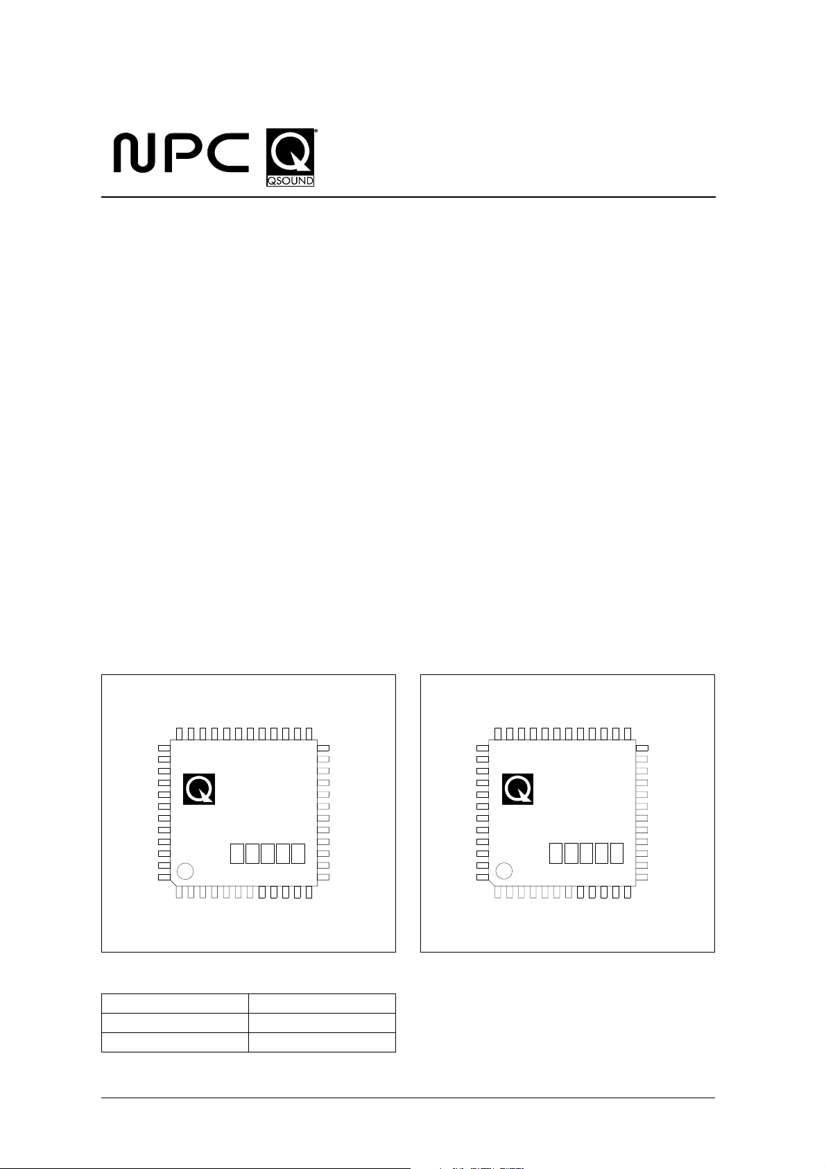
PINOUT (Top view)
QS7785PF QS7785CF
FROUT
QXBC3
QXBC4
27
28
10
MONO
SP(STRB)
26
11
AC
FLOUT
25
24
23
22
21
20
19
18
17
16
15
14
13
12
BYP(SDA)
SROUT
SLOUT
COUT
CIN
LPC
VREFIN
N.C.
VREFOUT
PSAVE
MUTE
BASS
SUR(SCL)
RIN
LIN
BASC2
MSC6
MSC5
MSC4
MSC3
MSC2
MSC1
QXCC1
QXCC2
QXCC3
37
38
39
40
41
42
43
44
45
46
47
48
RIN
LIN
BASC2
MSC6
MSC5
MSC4
MSC3
MSC2
MSC1
QXCC1
QXCC2
QXCC3
BASC1
QXAC1
QXAC2
QXAC3
QXAC4
VCC
31
32
33
34
35
36
37
38
39
40
41
42
43
44
QS7785PF
45
46
47
48
123456789
QXDC2
QXDC3
GND
QXDC4
QXCC4
QXDC1
QXBC1
29
30
VDD
QXBC2
P/S
ORDERING INFORMATION
BASC1
QXAC1
QXAC2
QXAC3
QXAC4
VCC
QXBC1
QXBC2
QXBC3
28
29
30
31
32
33
34
35
36
QS7785CF
123456789
SP
P/S
VDD
QXDC2
QXDC3
GND
QXDC4
QXCC4
QXDC1
QXBC4
26
27
10
11
MONO
FROUT
FLOUT
25
12
AC
BYP(SDA)
24
SROUT
23
SLOUT
22
COUT
21
CIN
20
LPC
19
VREFIN
18
N.C.
17
VREFOUT
16
PSAVE
15
MUTE
14
BASS
13
SUR(SCL)
Device Package
QS7785PF 48-pin QFP
QS7785CF 48-pin QFP
2
I
C bus is a registered trademark of Philips Electronics N.V.
Dolby and the double-D symbol are registered trademarks of Dolby Laboratories Licensing Corporation.
NIPPON PRECISION CIRCUITS—1
Page 2
PACKAGE DIMENSIONS
(Unit: mm)
QS7785PF/CF
0.20
0.20
7.00
9.00
0.50
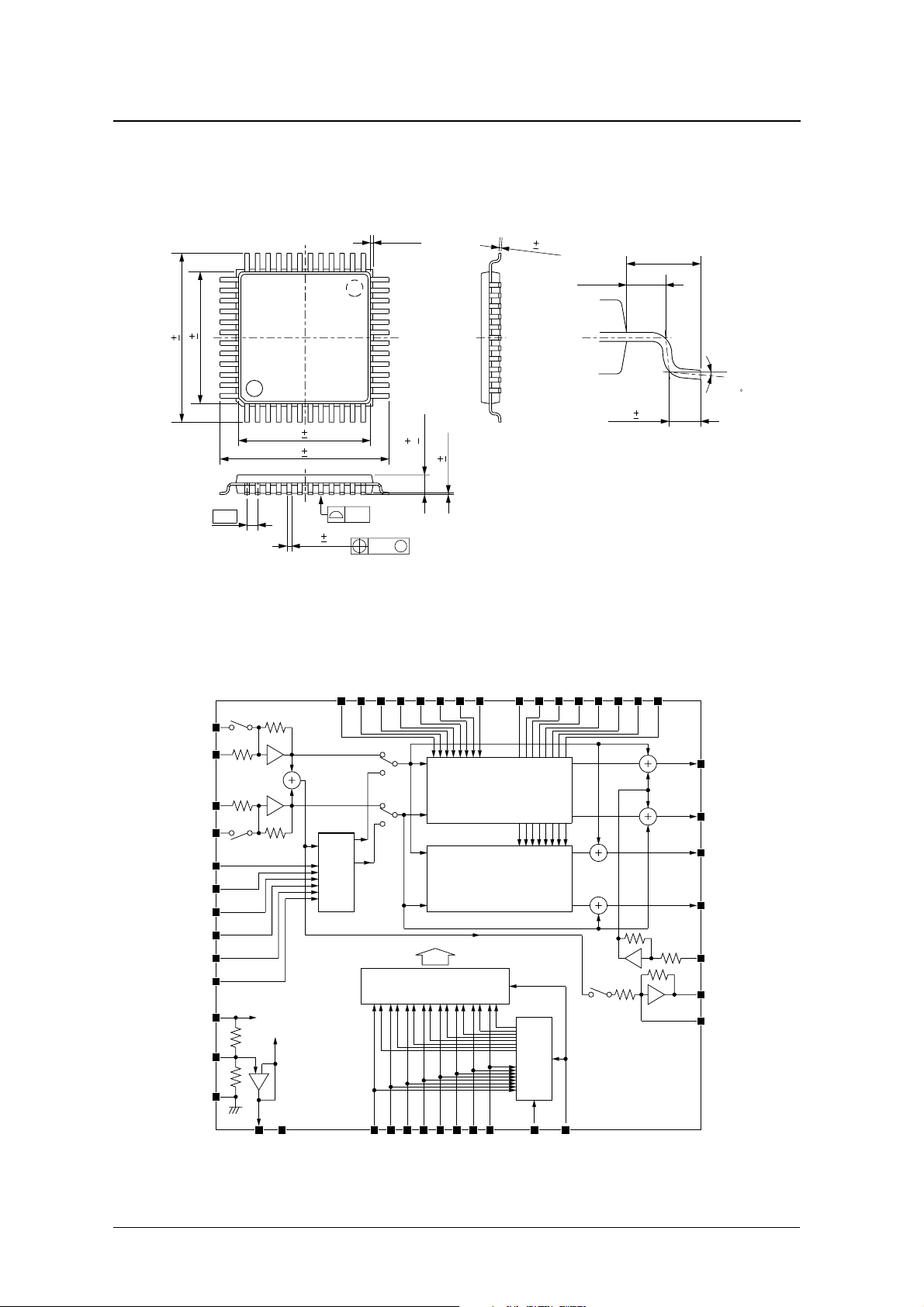
BLOCK DIAGRAM
7.00
9.00
0.19
0.20
0.20
0.05
0.10
0.35max
0.08
0.17
0.05
0.339typ
0.20
0.10
0.07
1.50
0.10
M
1.00typ
0 to 10
0.50 0.10
BASC1
RIN
LIN
BASC2
MSC6
MSC5
MSC4
MSC3
MSC2
MSC1
VCC
VREFIN
GND
QXAC2
QXAC4
QXBC2
QXBC4
QXCC1
QXBC3
QXBC1
QXAC3
QXAC1
293234 27 46 48 2 4
28
30
33
36
37
38
39
40
41
42
43
44
45
31
19
6
17
To internal
18
35
Mono to
Stereo
To internal
Multiplex/Decode/Level Shift
16
15
14
10AC11
Front
QEXPANDER
Surround
QEXPANDER
9
13
12
QXCC3
QXCC247QXCC4
135
Serial I/O
7
8
QXDC1
QXDC2
QXDC3
QXDC4
26
25
24
23
21
22
20
FROUT
FLOUT
SROUT
SLOUT
CIN
COUT
LPC
N.C.
VREFOUT
MUTE
PSAVE
BASS
MONO
SP(STRB)
SUR(SCL)
BYP(SDA)
VDD
P/S
NIPPON PRECISION CIRCUITS—2
Page 3
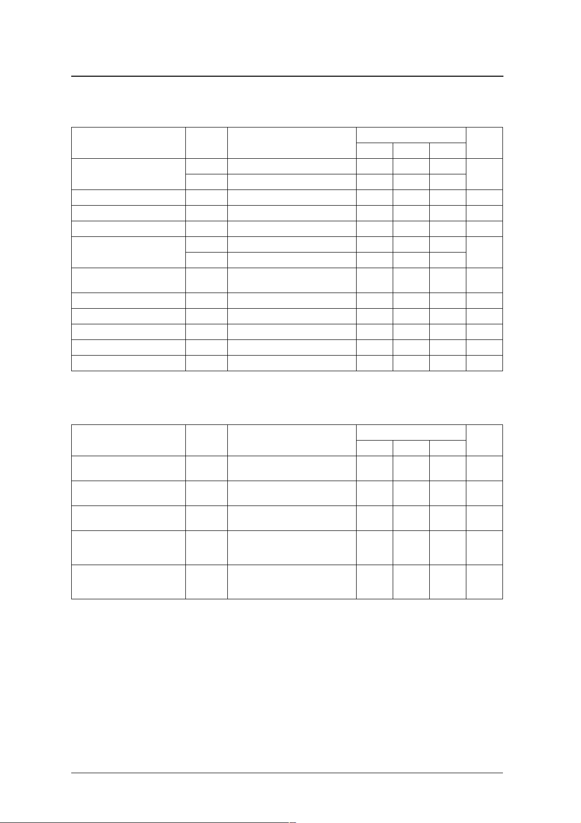
PIN DESCRIPTION
QS7785PF/CF
Number
I/O Description
Parallel Serial
1 QXCC4 O QEXPANDER C capacitor 4
2 QXDC1 I QEXPANDER D capacitor 1
3 QXDC2 O QEXPANDER D capacitor 2
4 QXDC3 I QEXPANDER D capacitor 3
5 QXDC4 O QEXPANDER D capacitor 4
6 GND – Ground
7 VDD – 4.5 to 5.5V digital supply
8 P/S I Input mode control (HIGH: parallel, LOW: serial)
SP – I Enhancement control (HIGH: high spread, LOW: low spread)
9
– STRB I Serial data strobe (not applicable to QS7785CF)
10 MONO I Mono-to-stereo convert select (HIGH: mono to stereo mode, LOW: normal mode)
11 AC I Center output control (HIGH: center on, LOW: center off)
BYP – I Bypass control (HIGH: bypass, LOW: Qsurround)
Name
12
– SDA I/O Serial data input (also serves as ACK signal output for I
2
C bus)
SUR – I Surround speaker control (HIGH: surround speaker on, LOW: off)
13
– SCL I Serial clock signal input
14 BASS I Bass boost mode control (HIGH: bass boost on, LOW: bass boost off)
15 MUTE I Mute signal control (HIGH: mute on, LOW: mute off)
16 PSAVE I Power save control (HIGH: power save on, LOW: power save off)
17 VREFOUT O V
/2 reference voltage output
CC
18 NC – No connection
19 VREFIN I V
/2 reference voltage output (biased internally to V
CC
/2)
CC
20 LPC I Center output lowpass filter
21 CIN I COUT output signal feedback input for front-channel output
22 COUT O Center signal output
23 SLOUT O Surround left-channel signal output
24 SROUT O Surround right-channel signal output
25 FLOUT O Front left-channel signal output
26 FROUT O Front right-channel signal output
27 QXBC4 O QEXPANDER B capacitor 4
28 QXBC3 I QEXPANDER B capacitor 3
29 QXBC2 O QEXPANDER B capacitor 2
30 QXBC1 I QEXPANDER B capacitor 1
31 VCC – 5 to 13V DC analog supply
32 QXAC4 O QEXPANDER A capacitor 4
33 QXAC3 I QEXPANDER A capacitor 3
34 QXAC2 O QEXPANDER A capacitor 2
35 QXAC1 I QEXPANDER A capacitor 1
36 BASC1 I Bass boost right-channel signal input
NIPPON PRECISION CIRCUITS—3
Page 4
−
−
−
−
−
° C
−
° C
QS7785PF/CF
Number
I/O Description
Parallel Serial
37 RIN I Right-channel signal input
38 LIN I Left-channel signal input
39 BASC2 I Bass boost left-channel signal input
40 MSC6 I Mono/stereo conversion filter capacitor 6
41 MSC5 I Mono/stereo conversion filter capacitor 5
42 MSC4 I Mono/stereo conversion filter capacitor 4
43 MSC3 I Mono/stereo conversion filter capacitor 3
44 MSC2 I Mono/stereo conversion filter capacitor 2
45 MSC1 I Mono/stereo conversion filter capacitor 1
46 QXCC1 I QEXPANDER C capacitor 1
47 QXCC2 O QEXPANDER C capacitor 2
48 QXCC3 I QEXPANDER C capacitor 3
SPECIFICATIONS
Absolute Maximum Ratings
GND = 0V
Name
Parameter Symbol Rating Unit
Supply voltage range (analog) V
Supply voltage range (digital) V
Input voltage range (analog) V
Input voltage range (digital) V
2
I
C signal input voltage (SDA, SCL) V
Power dissipation P
Storage temperature range T
Recommended Operating Conditions
GND = 0V
Parameter Symbol Rating Unit
Supply voltage range (analog) V
Supply voltage range (digital) V
Operating temperature range T
CC
DD
IANA
IDIG
IOPEN
D
stg
CC
DD
opr
0.3 to 15 V
0.3 to 7 V
0.3 to V
+ 0.3 V
CC
0.3 to V
+ 0.3 V
DD
10 V
250 mW
40 to 125
5 to 13 V
4.5 to 5.5 V
20 to 85
NIPPON PRECISION CIRCUITS—4
Page 5
DC Characteristics
V
= 9V, V
CC
= 5V, GND = 0V, Ta = 25 ° C
DD
−
−
QS7785PF/CF
Parameter Symbol Condition
Z
Analog input impedance
Reference voltage output V
HIGH-level input voltage V
LOW-level input voltage V
Input leakage current
LOW-level output voltage V
Supply voltage (analog) V
Supply voltage (digital) V
Current consumption (analog) I
Current consumption (digital) I
Standby current (analog) I
AIN1
Z
AIN2
REFOUT
IH
IL
I
LEAK
I
ILOPD
OL
CC
DD
CC
DD
CCSAVE
Noise and THD Characteristics
V
= 9V, V
CC
= 5V, GND = 0V, Ta = 25 ° C
DD
Rating
min typ max
LIN, RIN 16 20 24
CIN 8 10 12
–V
0.7V
DD
/2 – V
CC
––V
– – 0.3V
Digital inputs, V
SDA, SCL, 10V input voltage
ACK signal output from SDA, 3mA sink
current
input voltage
DD
3– 3
3– 3
0 – 0.4 V
5 – 13 V
4.5 – 5.5 V
–68mA
– 0.3 0.5 mA
– 0.1 0.2 mA
Unit
k Ω
DD
V
µA
Parameter Symbol Condition
Bypass noise voltage N
Qsurround noise voltage (front) N
Qsurround noise voltage (surround) N
Bypass total harmonic distortion THD
Qsurround mono total harmonic
distortion
THD
BYP = HIGH, SUR = MONO = SP = LOW,
BYP
“A”-wgt, FLOUT, FROUT
SUR = SP = HIGH, BYP = MONO = LOW,
QSF
“A”-wgt, FLOUT, FROUT
SUR = SP = HIGH, BYP = MONO = LOW,
QSR
“A”-wgt, SLOUT, SROUT
BYP = SUR = HIGH, MONO = SP = LOW,
LIN = RIN = 1V
B
FROUT, SLOUT, SROUT
, f = 1kHz, FLOUT,
RMS
BYP = LOW, SUR = MONO = SP = HIGH,
LIN = RIN = 1V
QM
FROUT, SLOUT, SROUT
, f = 1kHz, FLOUT,
RMS
Rating
Unit
min typ max
–1020µV
–2040µV
–1530µV
RMS
RMS
RMS
– – 0.1 %
– – 0.1 %
NIPPON PRECISION CIRCUITS—5
Page 6

AC Characteristics
V
= 9V, V
CC
= 5V, GND = 0V, Ta = 25 ° C
DD
QS7785PF/CF
−
−
−
−
−
−
−
−
−
Parameter Symbol Condition
Bypass-mode maximum input voltage V
Qsurround enhanced-mode
maximum input voltage
Qsurround-mode maximum input
voltage (surround speakers on)
Mono/stereo conversion enhanced
mode maximum input voltage
Mono/stereo conversion mode
maximum input voltage (surround
speakers on)
Bypass gain G
Bypass gain (surround speakers on) G
Qsurround mode gain G
Qsurround mode crosstalk gain G
Qsurround mode gain (surround) G
Qsurround mode crosstalk gain
(surround)
G
Qsurround enhanced mode gain G
Qsurround enhanced mode crosstalk
gain
Mono/stereo conversion mode leftchannel gain
Mono/stereo conversion mode rightchannel gain
Mono/stereo conversion enhanced
mode left-channel gain
Mono/stereo conversion enhanced
mode right-channel gain
G
Mono/stereo conversion mode
surround left-channel gain
Mono/stereo conversion mode
surround right-channel gain
G
SCL clock pulse period t
SCL clock HIGH-level pulsewidth t
SCL clock LOW-level pulsewidth t
SDA setup time t
SDA hold time t
STRB setup time t
STRB pulsewidth t
STRB hold time t
V
G
G
G
G
G
V
V
V
BYP1
BYP2
QXS
QX+
ML+
MR+
MSL
MSR
Rating
min typ max
BYP = SUR = HIGH, MONO = SP = LOW,
B
LIN = RIN, f = 1kHz
BYP = MONO = SUR = LOW, SP = HIGH,
Q+
LIN = RIN, f = 1kHz
BYP = MONO = SP = LOW, SUR = HIGH,
QS
LIN = RIN, f = 1kHz
BYP = SUR = LOW, MONO = SP = HIGH,
M+
LIN = RIN, f = 1kHz
BYP = SP = LOW, MONO = SUR = HIGH,
MS
LIN = RIN, f = 1kHz
BYP = HIGH, MONO = SUR = SP = LOW,
LIN to FLOUT, RIN to FROUT, f = 1kHz
BYP = SUR = HIGH, MONO = SP = LOW,
LIN to SLOUT, RIN to SROUT, f = 1kHz
BYP = MONO = SUR = SP = LOW, LIN to
Q
FLOUT, RIN to FROUT, f = 1kHz
BYP = MONO = SUR = SP = LOW, LIN to
QX
FROUT, RIN to FLOUT, f = 1kHz
BYP = MONO = SP = LOW, SUR = HIGH,
QS
LIN to SLOUT, RIN to SROUT, f = 1kHz
BYP = MONO = SP = LOW, SUR = HIGH,
LIN to SROUT, RIN to SLOUT, f = 1kHz
BYP = MONO = SUR = LOW, SP = HIGH,
Q+
LIN to FLOUT, RIN to FROUT, f = 1kHz
BYP = MONO = SUR = LOW, SP = HIGH,
LIN to FROUT, RIN to FLOUT, f = 1kHz
BYP = SUR = SP = LOW, MONO = HIGH,
ML
LIN = RIN, FLOUT, f = 1kHz
BYP = SUR = SP = LOW, MONO = HIGH,
MR
LIN = RIN, FROUT, f = 1kHz
BYP = SUR = LOW, MONO = SP = HIGH,
LIN = RIN, FLOUT, f = 1kHz
BYP = SUR = LOW, MONO = SP = HIGH,
LIN = RIN, FROUT, f = 1kHz
BYP = SP = LOW, MONO = SUR = HIGH,
LIN = RIN, SLOUT, f = 1kHz
BYP = SP = LOW, MONO = SUR = HIGH,
LIN = RIN, SROUT, f = 1kHz
QS7785PF 100 – – ns
0
QS7785PF 40 – – ns
1
QS7785PF 40 – – ns
2
QS7785PF 15 – – ns
3
QS7785PF 30 – – ns
4
QS7785PF 50 – – ns
5
QS7785PF 100 – – ns
6
QS7785PF 50 – – ns
7
1.7 2.3 – V
1.8 2.4 – V
1.3 1.7 – V
0.8 1.0 – V
0.8 1.0 – V
20 2dB
20 2dB
3.9 5.9 7.9 dB
1.5 0.5 2.5 dB
2.3
0.3 1.7 dB
1.9 0.1 2.1 dB
4.7 6.7 8.7 dB
1.3 3.3 5.3 dB
2.6 4.6 6.6 dB
3.6 5.6 7.6 dB
2.4 4.4 6.4 dB
3.3 5.3 7.3 dB
3.8
1.8 0.2 dB
1.6 0.4 2.4 dB
Unit
RMS
RMS
RMS
RMS
RMS
NIPPON PRECISION CIRCUITS—6
Page 7

QS7785PF/CF
Parameter Symbol Condition
SCL hold time (I
SCL setup time (I
SDA hold time (I
SDA setup time (I
SCL clock HIGH-level pulsewidth
2
(I
C)
SCL clock LOW-level pulsewidth (I
2
C) t
2
C) t
2
C) t
2
C) t
2
C) t
SCL rise time (I2C) t
2
SCL fall time (I
C) t
Serial Interface Timing
3-wire (QS7785PF) timing
SDA
SCL
STRB
BYP SP MONO AC
t
3
Rating
min typ max
HD:STA
SU:STO
HD:DAT
SU:DAT
t
HIGH
LOW
SUR BASS MUTE PSAVE
QS7785CF 4.0 – – µs
QS7785CF 4.0 – – µs
QS7785CF 5.0 – – µs
QS7785CF 250 – – ns
QS7785CF 4.0 – – µs
QS7785CF 4.7 – – µs
QS7785CF – – 1000 ns
r
QS7785CF – – 300 ns
f
t
4
t
1
t
2
t
0
Unit
t
6
t
t
5
7
Pin Description
SDA Data signal. Sets mode settings. See “Operating Modes.”
SCL Clock signal. Data is read on the rising edge.
STRB Strobe signal. Mode switches occur on the rising edge of this signal.
2
I
C 2-wire (QS7785CF) timing
2
I C address is {AD6 − AD0} = {1011011}
SDA
SCL
t
HD:STA
t
HIGH
AD0AD6
t
r
t
f
t
LOW
BYP SP
SUR
t
SU:DAT
t
HD:DAT
MONO
AC BASS MUTE PSAVE
t
SU:STO
Pin Description
SDA Data signal. Sets slave address and mode settings. Address value, {1011011}, is shown in the figure above. See “Operating Modes.”
SCL Clock signal. Data is read on the rising edge.
NIPPON PRECISION CIRCUITS—7
Page 8

FUNCTIONAL DESCRIPTION
Operating Modes
QS7785PF/CF
The QS7785PF/CF operating mode can be controlled over either a parallel interface (P/S = HIGH)
or one of two serial interfaces (P/S = LOW). The
operating mode, control pins and SDA signal relationship is shown in the table below. Refer to “Serial
Interface Timing” for the SDA signal format.
Output mode
No. Input signals
1
2 0001 Stereo Q+ –
3 0010 Stereo Q Stereo Q1
4 0011 Stereo Q+ Stereo Q1
5
6 0101 Mono → Stereo Q+ –
7 0110 Mono → Stereo Q Mono → Stereo Q1
8 0111 Mono → Stereo Q+ Mono → Stereo Q1
9
10 101× Stereo bypass Stereo bypass
11 110× – Stereo bypass
12 Stereo only 1 1 1 × Stereo bypass Stereo Q1
1. – (dash) = no output signal.
× = indicates don’t care.
1 = HIGH, 0 = LOW
Stereo only
Mono only
Stereo/Mono
Control pins/SDA signal Output signals
BYP MONO SUR SP FROUT/FLOUT SROUT/SLOUT
0000 Stereo Q –
0100 Mono → Stereo Q –
100× Stereo bypass –
1
Output signal description
Output signal Description
Stereo Q Mixed front-channel Qsurround processed signal and input stereo signal output
Stereo Q+ Same as Stereo Q with increased Qsurround signal component and reduced input stereo signal component.
Stereo Q1 Mixed surround-channel Qsurround processed signal and input stereo signal output.
Mono → Stereo Q Mono signal converted to vir tual stereo signal, and then processed in the same way as Stereo Q signals.
Mono → Stereo Q+ Mono signal converted to virtual stereo signal, and then processed in the same way as Stereo Q+ signals.
Stereo bypass Input stereo signal is output as-is without processing.
Mono signals should be input on both LIN and RIN.
In output mode 1, the output signal is a mixed signal
comprising the front-channel Qsurround processed
signal and the input stereo signal, that is output on
the 2-channel front speakers only.
In output mode 2, the signal path is the same as in
output mode 1, but the surround effect is enhanced
by increasing the component of the Qsurround processed signal and reducing the component of the
input stereo signal.
In output modes 3 and 4, both the front speakers and
tem for a rich surround space. The front-channel signal is the same as in output modes 1 and 2. The
surround-channel signal is a mixed signal comprising an enhanced surround effect Qsurround processed signal and the input stereo signal.
In output modes 5 to 8, the input signal is a mono
signal. The mono signal is first converted to a virtual
stereo signal and then processed in the same way as
in output modes 1 to 4, respectively. In modes 5 and
6, the surround signal is output on 2-channel front
speakers only. In modes 7 and 8, the surround signals
are output on 4-channel front and surround speakers.
surround speakers are used to form a 4-channel sys-
NIPPON PRECISION CIRCUITS—8
Page 9

QS7785PF/CF
In output modes 9 to 11, the input stereo signal is
output to the speakers without processing. The
bypass function works for both stereo and mono
input signals, and is used to listen to the original signals. In mode 9, the stereo signal is output on front
speakers only. In mode 10, the stereo signal is output
on both front and surround speakers. In mode 11, the
stereo signal is output on surround speakers only.
In output mode 12, the input stereo signal is output
on front speakers, and a surround effect enhanced
signal is output on the surround speakers.
Center signal output
Control pins/SDA signal
BYP MONO SUR SP AC COUT
××××0–
××××1 (RIN + LIN) / 2
1. – (dash) = no output signal.
× = indicates don’t care.
1 = HIGH, 0 = LOW
1
Output signal
The center signal is output on COUT. See “Center Control.”
Bass boost mode
Control pins/SDA signal
BYP MONO SUR SP AC BASS FROUT/FLOUT SROUT/SLOUT COUT
ЧЧЧЧЧ0 Bass boost OFF Bass boost OFF Bass boost OFF
ЧЧЧЧЧ1 Bass boost ON Bass boost ON Bass boost ON
1. × = indicates don’t care.
1 = HIGH, 0 = LOW
1
Output signal
The bass boost function is used to enhance the bass frequency component. See “Bass Boost.”
Mute and power save
Control pins/SDA signal
BYP MONO SUR SP AC BASS MUTE PSAVE FROUT/FLOUT SROUT/SLOUT COUT
ЧЧЧЧЧЧ0 0 Available Available Available
ЧЧЧЧЧЧ10–––
ЧЧЧЧЧЧ11–––
1. – (dash) = no output signal.
× = indicates don’t care.
1 = HIGH, 0 = LOW
1
Output signal
When PSAVE is HIGH, the analog stages of the
device are turned OFF to save power. When MUTE
is HIGH, all outputs are muted.
NIPPON PRECISION CIRCUITS—9
Page 10

QS7785PF/CF
Speaker Arrangement
The QS7785PF/CF supports the following speaker arrangements.
RIN
LIN
SROUT
FROUT
CIN
COUT
FLOUT
SLOUT
24
26
21
22
25
23
Front
Speakers
Rear
Speakers
37
38
Type A. Two front speakers in front and two surround
speakers in rear
24
SROUT
RIN
37
38
LIN
FROUT
CIN
COUT
FLOUT
SLOUT
26
21
22
25
23
24
SROUT
RIN
37
38
LIN
FROUT
CIN
COUT
FLOUT
SLOUT
26
21
22
25
23
Type B. Front speakers and surround speakers in
front
24
SROUT
RIN
37
38
LIN
FROUT
CIN
COUT
FLOUT
SLOUT
26
21
22
25
23
Type C. Front speakers and surround speakers in
front with actual center speaker
Type A
The front speakers are placed in front and the surround speakers are placed behind the audience to
create a full rich enhanced space. Since the output
signal for each channel has undergone Qsurround
processing, the audio enhancement can be reduced to
an adequate level even for television and similar signals where the left and right channels are located
close to each other.
Type B
The front speakers and surround speakers are both
placed in front of the audience, perhaps because it is
not possible to place speakers behind the audience. If
the surround speakers are turned to face outwards, to
spread the surround signal, the surround effect can
be obtained.
Type D. Front speakers and surround speakers in
front with center
Type C
A center speaker can be added in the center to reproduce vocal and speech signals for easy listening. The
center signal is output on COUT. The signal is comprised of LIN and RIN signals, producing a sound
image in the center.
Type D
If a center speaker is not available or not required,
COUT can be connected to CIN using a resistor and
the center signal is then added to the front-channel
signal. The presence of the center signal added to the
front channels reproduces the center signal sound
image with virtually the same effect as that obtained
using a center speaker. The connection using a resistor can be utilized for voice and similar fixed-band
signals. See “Center Control” for a description of the
method.
NIPPON PRECISION CIRCUITS—10
Page 11

Center Control
QS7785PF/CF
The center signal output on COUT is enabled when
AC is HIGH.
This section describes the output function whereby
fixed frequency sound sources, such as vocal and
speech signals, can be output on the center signal. As
mentioned for “Type C” and “Type D” speaker
arrangements, the center signal can be output by
direct connection to a speaker or by adding the signal
to the front-channel output using a resistor connection between CIN and COUT.
Using a center speaker
When using a speaker, a capacitor Ca can be connected between LPC and COUT, forming a lowpass
filter. The −3dB cutoff frequency of the filter is given
by the following equation.
f
1
---------------------------=
2π Ca R1×
Frequencies higher than voice tones are cut from the
signal sent to the center speaker for clear reproduction of voice-band signals.
Adding to the front-channel output
With this connection, the bass frequency components
can be removed from a signal. Capacitors Ca and Cb
and resistor Ra can be connected between CIN and
COUT to form a highpass filter. The −3dB cutoff frequency of the filter is given by the following equation.
f
----------------------------------------=
2π Cb Ra R2+()
1
The input signal on CIN is added equally to both
front-channel outputs FLOUT and FROUT. Frequencies lower than voice tones are cut from the signal
added to the front-channel outputs for clear reproduction of voice-band signals.
Close when AC=H
Open when AC=L
R1:20k
LPC
20
22
COUT
−6dB
GC
Ca
Ra:10k
Cb:0.082µF
CIN
21
Center output connection
V(COUT)/V(RIN)@V(LIN)=0
Gain
3dB
fL fH
Close when MUTE=H
Open when MUTE=L
R3:10k
R2:10k
3dB
fL=
G
V(FROUT)
or V(FLOUT)
Freq.
10k
10k
1
2πCb(Ra+R2)
C=20 log
REFOUT
V
FROUT
26
10k
10k
FLOUT
25
1
fH=
2πCaR1
R3
Ra+R2
−6dB
()
Front Right
Speaker
Cnter
Speaker
Front Left
Speaker
Center output frequency response
Note: Internal resistance value, R1 and R2, may vary ± 15%.
NIPPON PRECISION CIRCUITS—11
Page 12

Bass Boost
QS7785PF/CF
With a signal input connected to BASC1 and
BASC2, a bass boost function can be implemented.
When BASS is HIGH, resistors RA and RB and
RIN
+
RA=10k
/LIN
37
RB:10k
36
C:0.15µF
BASC1
/BASC2
Bass boost connection (Gb = 6dB, fC = 300Hz)
.
Gain
Gb
0dB
f
L fH
fC
capacitor C are connected to form a lowpass filter.
The lowpass filter signal and the original signal
(RIN, LIN) are combined to boost bass frequencies.
R1:20k
Freq.
R2:20k
V
REFOUT
Close when BASS=H
Open when BASS=L
Gb=20 log
1+
C=
f
2πC
1
−
fL=fC 10
fH=fC 10
2
1
2
To Internal
R1
1+
()
RA+RB
R1
RA+RB
RA RB
RA+RB
R1
1+
log
()
RA+RB
RA+RB
1+2
R1
R1
1+
log
()
RA+RB
RA+RB
1+2
R1
Bass boost frequency response
NIPPON PRECISION CIRCUITS—12
Page 13

TYPICAL APPLICATIONS
Parallel Interface
10k 10k
4.7µF
Signal In
4.7µF
10k 10k
0.15µF
0.022µF
2700pF
0.082µF
0.012µF
1000pF
8200pF
0.22µF
QXCC2
QXCC3
8200pF
0.15µF
RIN
LIN
QS7785PF/CF
5 to 13V
0.01µF
0.01µF 3300pF 3300pF
36
3534333231302928272625
37
BASC1
38
BASC2
39
MSC6
40
MSC5
41
MSC4
42
MSC3
43
MSC2
44
MSC1
45
QXCC1
46
47
48
QXCC4
123456789
QXAC1
QXAC2
QXDC2
QXDC1
QXAC3
QXDC3
8200pF8200pF
QXAC4
QXDC4
VCC
GND
QXBC1
QXBC2
VDD
P/S
QXBC3
QXBC4
VREFIN
VREFOUT
MONO
SP(STRB)
101112
FROUT
COUT
CIN
LPC
N.C.
PSAVE
AC
SROUT
24
SLOUT
23
FLOUT
22
21
20
19
18
17
16
MUTE
15
BASS
14
13
BYP(SDA)
SUR(SCL)
10µF
10µF
4.7µF
4.7µF
4.7µF
4.7µF
4.7µF
Signal Out
47k
5V
A capacitor for decoupling should be connected between supply and ground.
NIPPON PRECISION CIRCUITS—13
Page 14

Serial Interface
QS7785PF
Signal In
4.7µF
4.7µF
10k 10k
10k 10k
0.15µF
0.22µF
0.022µF
2700pF
0.082µF
0.012µF
1000pF
8200pF
QXCC2
QXCC3
8200pF
0.15µF
RIN
LIN
QS7785PF/CF
5 to 13V
0.01µF 3300pF 3300pF
0.01µF
36
3534333231302928272625
37
BASC1
38
BASC2
39
MSC6
40
MSC5
41
MSC4
42
MSC3
43
MSC2
44
MSC1
45
QXCC1
46
47
48
QXCC4
123456789
QXAC1
QXAC2
QXDC2
QXDC1
QXAC3
QXDC3
8200pF8200pF
QXAC4
QXDC4
VCC
GND
QXBC1
QXBC2
VDD
P/S
QXBC3
QXBC4
VREFIN
VREFOUT
MONO
SP(STRB)
101112
FROUT
COUT
CIN
LPC
N.C.
PSAVE
AC
SROUT
24
SLOUT
23
FLOUT
22
21
20
19
18
17
16
MUTE
15
BASS
14
SUR(SCL)
13
BYP(SDA)
4.7µF
4.7µF
10µF
10µF
4.7µF
4.7µF
4.7µF
Signal Out
SCL
SDA
STRB
QS7785PF
Signal In
4.7µF
4.7µF
10k 10k
10k 10k
0.15µF
0.22µF
0.022µF
2700pF
0.082µF
0.012µF
1000pF
8200pF
QXCC2
QXCC3
8200pF
0.15µF
RIN
LIN
5 to 13V
0.01µF
0.01µF 3300pF 3300pF
36
3534333231302928272625
37
BASC1
38
39
40
41
42
43
44
45
46
BASC2
MSC6
MSC5
MSC4
MSC3
MSC2
MSC1
QXCC1
QXAC1
QXAC2
QXAC3
QXAC4
47
48
QXDC1
QXCC4
QXDC2
QXDC3
QXDC4
123456789
8200pF8200pF
5V
VCC
GND
QXBC1
QXBC2
VDD
P/S
QXBC3
QXBC4
VREFOUT
MONO
SP
101112
FROUT
COUT
CIN
LPC
VREFIN
N.C.
PSAVE
AC
SROUT
24
SLOUT
23
FLOUT
22
21
20
19
18
17
16
MUTE
15
BASS
14
SUR(SCL)
13
BYP(SDA)
10µF
10µF
4.7µF
4.7µF
4.7µF
4.7µF
4.7µF
Signal Out
SCL
SDA
5V
A capacitor for decoupling should be connected between supply and ground.
NIPPON PRECISION CIRCUITS—14
Page 15

QS7785PF/CF
NIPPON PRECISION CIRCUITS INC. reserves the right to make changes to the products described in this data sheet in order to
improve the design or performance and to supply the best possible products. Nippon Precision Circuits Inc. assumes no responsibility for
the use of any circuits shown in this data sheet, conveys no license under any patent or other rights, and makes no claim that the circuits
are free from patent infringement. Applications for any devices shown in this data sheet are for illustration only and Nippon Precision
Circuits Inc. makes no claim or warranty that such applications will be suitable for the use specified without further testing or modification.
The products described in this data sheet are not intended to use for the apparatus which influence human lives due to the failure or
malfunction of the products. Customers are requested to comply with applicable laws and regulations in effect now and hereinafter,
including compliance with export controls on the distribution or dissemination of the products. Customers shall not export, directly or
indirectly, any products without first obtaining required licenses and approvals from appropriate government agencies.
NIPPON PRECISION CIRCUITS INC.
4-3, Fukuzumi 2-chome
Koto-ku, Tokyo 135-8430, Japan
Telephone: +81-3-3642-6661
NIPPON PRECISION CIRCUITS INC.
Facsimile: +81-3-3642-6698
http://www.npc.co.jp/
Email: sales
@npc.co.jp
NIPPON PRECISION CIRCUITS—15
NC9818BE 2000.11
 Loading...