

Page 1
QS7779PM/CM
3D Stereo Enhancement and 3D Virtual Stereo Surround
NIPPON PRECISION CIRCUITS INC.
OVERVIEW
with Dolby Pro Logic and Mixed DVD (AC-3) Decoder
The QS7779PM/CM is an audio processor IC which
implements a decoder for stereo matrix encoded
source materials such as the Dolby Surround Pro
Logic and mixed DVD (AC − 3) with surround virtualization using QSound technology developed and
licensed by QSound Labs, Inc. This chip produces
enhanced stereo sound for a stereo input signal and if
the input signal contains matrix encoded surround
sound, the chip decodes it and produces 3D virtualized surround sounds with two speakers.
FEATURES
■
Capable of decoding Dolby Surround materials
such as Dolby Pro Logic or other matrix surround
encoded materials (DVD/AC − 3)
■
Virtualized surround sound with two speakers
■
3D stereo sound enhancement
■
Two enhanced levels
■
Parallel and serial digital interface for mode con-
• QS7779CM for I
face (Data, Clock)
• QS7779PM for three-wire serial interface
(Data, Clock and Strobe)
■
Supply voltage (analog): 5 to 13V
Supply voltage (digital): 4.5 to 5.5V
■
24-pin SSOP packaging
trol
APPLICATIONS
■
DVD, Laser disk player
■
Audio systems including TV, Radio and VCR
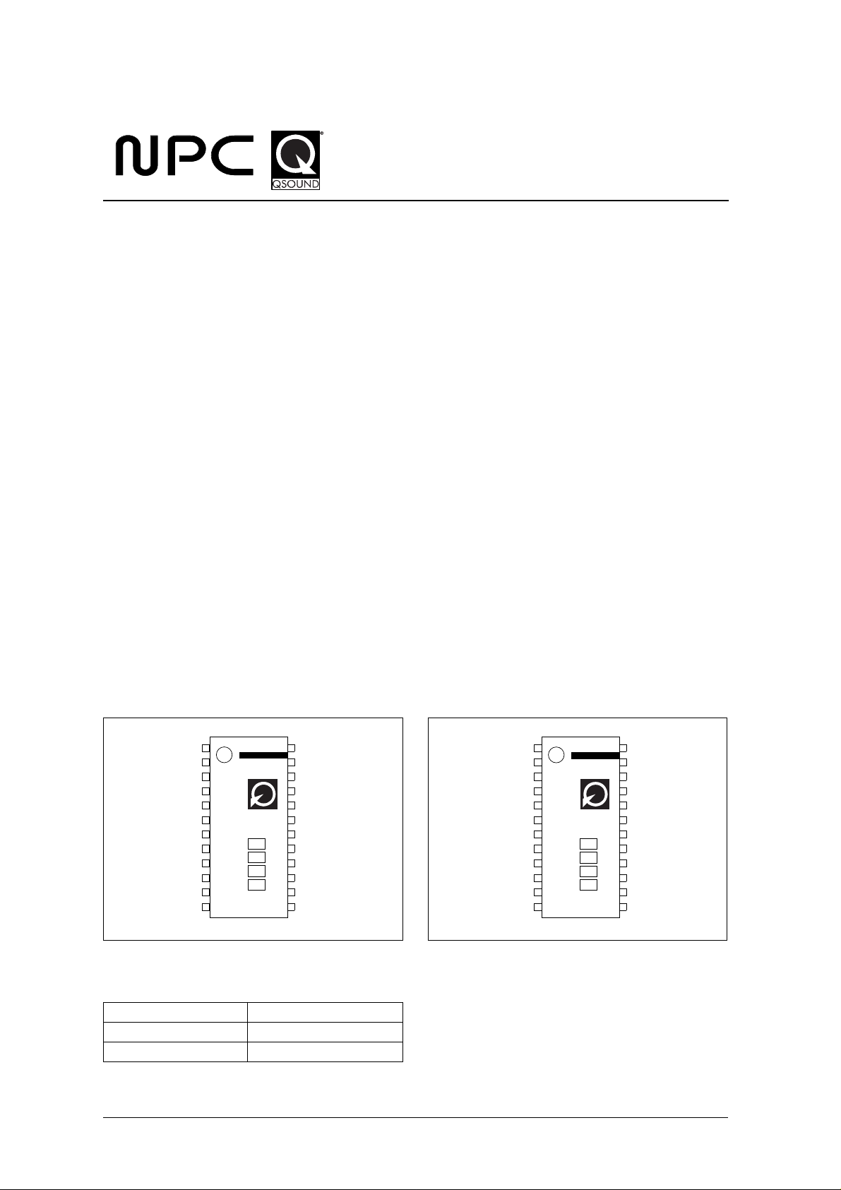
PINOUT
(Top view)
QS7779PM QS7779CM
■
Computer-based multimedia products, including
sound cards and powered loudspeakers
2
C 2 control pins serial inter-
QXAC3
QXAC2
QXAC1
RIN
LIN
COUT
CIN
VREFIN
VREFOUT
VREF
GND
SPRD(SCL)
1
QS7779PM
12
24
QXAC4
VCC
QXBC1
QXBC2
QXBC3
QXBC4
ROUT
LOUT
MUTE(STRB)
VDD
P/S
BYP(SDA)
13
Using these products does not require any Dolby certifications.
QXAC3
QXAC2
QXAC1
RIN
LIN
COUT
CIN
VREFIN
VREFOUT
VREF
GND
SPRD(SCL)
ORDERING INFORMATION
De vice Pack ag e
QS7779PM 24-pin SSOP
QS7779CM 24-pin SSOP
2
I
C bus is a registered trademark of Philips Electronics N.V.
Dolby and the double-D symbol are registered trademarks of Dolby Laboratories Licensing Corporation.
1
QS7779CM
12
NIPPON PRECISION CIRCUITS—1
24
13
QXAC4
VCC
QXBC1
QXBC2
QXBC3
QXBC4
ROUT
LOUT
MUTE
VDD
P/S
BYP(SDA)
Page 2
PACKAGE DIMENSIONS
(Unit: mm)
10.05 0.20
10.20 0.30
QS7779PM/CM
7.80 0.30
5.40 0.20
0.15
0.10
+
−
0.05
0.8
BLOCK DIAGRAM
RIN
4
LIN
5
23
VCC
GND
8
11
VREFIN
1.80
0.36 0.10
0.10
QXAC1QXAC2QXAC3QXAC4QXBC1 QXBC2QXBC3 QXBC4
123 2422212019
Surround
Decoder
910 121316
VREFOUT VREF
M
0.12
0.10 0.10
QXpander
Q1
Virtualization
Multiplex/Level Shift
BYP
(SDA)
MUTE
(STRB)
SPRD
(SCL)
+0.20
−0.10
1.90
0.50 0.20
Σ
Σ
Serial I/O
010
18
ROUT
17
LOUT
7
CIN
6
COUT
14
P/S
15
VDD
NIPPON PRECISION CIRCUITS—2
Page 3
PIN DESCRIPTION
QS7779PM/CM
Number
I/O Description
Parallel Serial
1 Q X A C 3 I Capacitor 3 for QEXPANDER filter A
2 Q X A C 2 I Capacitor 2 for QEXPANDER filter A
3 Q X A C 1 I Capacitor 1 for QEXPANDER filter A
4 RI N I Right channel signal input
5 LIN I Left channel signal input
6 COUT O Decoded center signal output
7 CI N I Center signal input for summing with the right and the left signal outputs
Name
8 VREFIN O
9 VREFOUT O
Internally generated reference voltage (V
Buffered reference voltage (V
CC
/2)
CC
/2)
10 VREF I Signal reference input
11 GN D – Ground 0V
SPRD – I Enhancement control (H: spread maximum, L: spread minimum )
12
–
SCL
1
I Se r ial data shift clock
B Y P – I Bypass control (H: Bypass on, L: Qsurround on)
13
–
SDA
2
I/O
Se r ial data input. ACK data output for I
2
C (QS7779CM)
14 P/S I Interface mode control (H: parallel I/O, L: serial I/O)
15 V DD – Digital pow e r supply DC4.5 to 5.5V
MUTE – I Output mute control (H: m ute on, L: m ute off)
16
– STRB I
Ser ial data strobe (not applicable to I
2
C of QS7779CM)
17 LOUT O Left signal output
18 R OUT O Right signal output
19 QXBC4 I Capacitor 4 fo r QEXPANDER filter B
20 QXBC3 I Capacitor 3 fo r QEXPANDER filter B
21 QXBC2 I Capacitor 2 fo r QEXPANDER filter B
22 QXBC1 I Capacitor 1 fo r QEXPANDER filter B
23 VC C – Analog power supply DC5 to 13V
24 QXA C 4 I Capacitor 4 for QEXPANDER filter A
1. QS7779CM:CMOS input. No protective diode between the terminal and V D D.
QS7779PM:CMOS input. Protective diode is in between the terminal and V D D.
2. QS7779CM:Nch open drain terminal. No protective diode between terminal and V D D.
QS7779PM:CMOS input. Protective diode is in between the terminal and V D D.
NIPPON PRECISION CIRCUITS—3
Page 4
SPECIFICATIONS
Absolute Maximum Ratings
GND = 0V
Parameter Symbol Rating Unit
Supply voltage (analog)
Supply voltage (digital)
Input voltage (analog)
Input voltage (digital)
2
I
C input voltage (SDA, SCL)
Po w er dissipation
Storage temperature
Soldering temperature
Soldering time
V
V
V
IANA
V
IDIG
V
IOPEN
P
T
T
SLD
t
SLD
CC
DD
D
stg
°
°
°
QS7779PM/CM
– 0.3 to 15 V
– 0.3 to 7 V
– 0.3 to V
– 0.3 to V
+ 0.3
CC
+ 0.3
DD
10 V
250 m W
– 40 to 125
255
10 sec
V
V
C
C
Recommended Operating Conditions
GND = 0V
Parameter Symbol Limits Unit
Supply voltage (analog)
Supply voltage (digital)
Operating temperature
V
V
T
CC
DD
OPR
5 to 13
4.5 to 5.5 V
– 20 to 70
V
C
NIPPON PRECISION CIRCUITS—4
Page 5
DC Electrical Characteristics
V
= 9V, V
CC
= 5V, GND = 0V, Ta = 25 ° C unless otherwise noted.
DD
QS7779PM/CM
Ω
Ω
×
×
µ
µ
µ
µ
Parameter
LIN, RIN analog input impedance
CIN analog input impedance
Reference voltage out
HIGH-level input voltage
L O W -level input voltage
Input leakage current
S DA, SCL input leakage current
2
(I
C input pin)
S D A L OW -level output voltage
Supply voltage (analog)
Supply voltage (digital)
Current consumption (analog)
Current consumption (digital)
Standby current (analog)
Symbol Condition
Z
AIN1
Z
AIN2
V
REFOUT
V
IH
V
IL
I
LEAK
I
LOPEN
I
CCSAVE
V
= 10V
IN
Acknowledge signal out
V
OL
I
= 3mA
OL
V
CC
V
DD
I
CC
I
DD
Limits
Unit
min typ max
16 20 24 k
456k
V
–
0.7
V
DD
––
– 3 – 3
– 3 – 3
CC
/2
–V
––V
V
0.3
DD
V
A
A
0 – 0.4 V
5–13V
4.5 – 5.5 V
– 5 6.5 m A
– 0.3 0.5 mA
– 0.1 0.2 mA
Noise/THD Characteristics
V
= 9V, V
CC
Noise voltage
Noise voltage
THD
= 5V, GND = 0V, Ta = 25 ° C unless otherwise noted.
DD
Parameter
Symbol Condition
N
BYP
N
THD
BYP = HIGH (Bypass mode), A-wgt,
LOUT, ROUT
BYP = LOW (Qsurround mode),
QS
SPRD = HIGH, A-wgt, LOUT, RO UT
LIN = RIN = 1V
QS
round mode), SPRD = HIGH, f = 1kHz
, BYP = LOW (Qsur-
RMS
Limits
min typ max
–1020
–2040
– – 0.1 %
Unit
V
RMS
V
RMS
NIPPON PRECISION CIRCUITS—5
Page 6
AC Electrical Characteristics
V
= 9V, V
CC
= 5V, GND = 0V, Ta = 25 ° C unless otherwise noted.
DD
QS7779PM/CM
µ
µ
µ
µ
µ
Parameter
Maximum input voltage 1
Maximum input voltage 2
Bypass gain
Forward gain
Crosstalk gain
SCL clock pulse cycle
SCL HIGH-level clock pulse width
SCL LOW-level clock pulse width
S DA set-up time
S DA hold time
STRB set-up time
STRB clock pulse width
STRB hold time
2
SCL hold time (I
SCL set-up time (I
S D A hold time (I
S D A set-up time (I
C)
2
C)
2
C)
2
C)
SCL HIGH-level clock pulse width
2
(I
C)
SCL LOW-level clock pulse width
2
(I
C)
SCL rise time (I
SCL fall time (I
2
C)
2
C)
Symbol Condition
V
V
G
t
HD:STA
t
SU:STO
t
HD:DAT
t
SU:DAT
t
t
LIN = RIN, BYP = LOW, SPRD = HIGH,
FIN1
f = 1kHz
LIN = – RIN, BYP = LOW, SPRD = HIGH,
FIN2
f = 1kHz
BYP = HIGH, f = 1kHz, LIN to LOUT,
BYP
RIN to ROU T
SPRD = HIGH, BYP = LOW, f = 1kHz,
G
F
LIN to LOUT, RIN to ROUT
SPRD = HIGH, BYP = LOW, f = 1kHz,
G
XF
LIN to ROUT, RIN to LOUT
t
PM version 100 – – ns
0
t
PM version 40 – – ns
1
t
PM version 40 – – ns
2
t
PM version 15 – – ns
3
t
PM version 30 – – ns
4
t
PM version 50 – – ns
5
t
PM version 100 – – ns
6
t
PM version 50 – – ns
7
CM version 4.0 – –
CM version 4.0 – –
CM version 5.0 – –
CM version 250 – – n s
CM version 4.0 – –
HIGH
CM version 4.7 – –
LOW
t
CM version – – 1000 ns
r
t
CM version – – 300 n s
f
Limits
Unit
min typ max
1.4 – –
0.5 – –
V
V
– 2 0 2 dB
6.6 8.6 10.6 d B
0.5 2.5 4.5 dB
RMS
RMS
s
s
s
s
s
NIPPON PRECISION CIRCUITS—6
Page 7
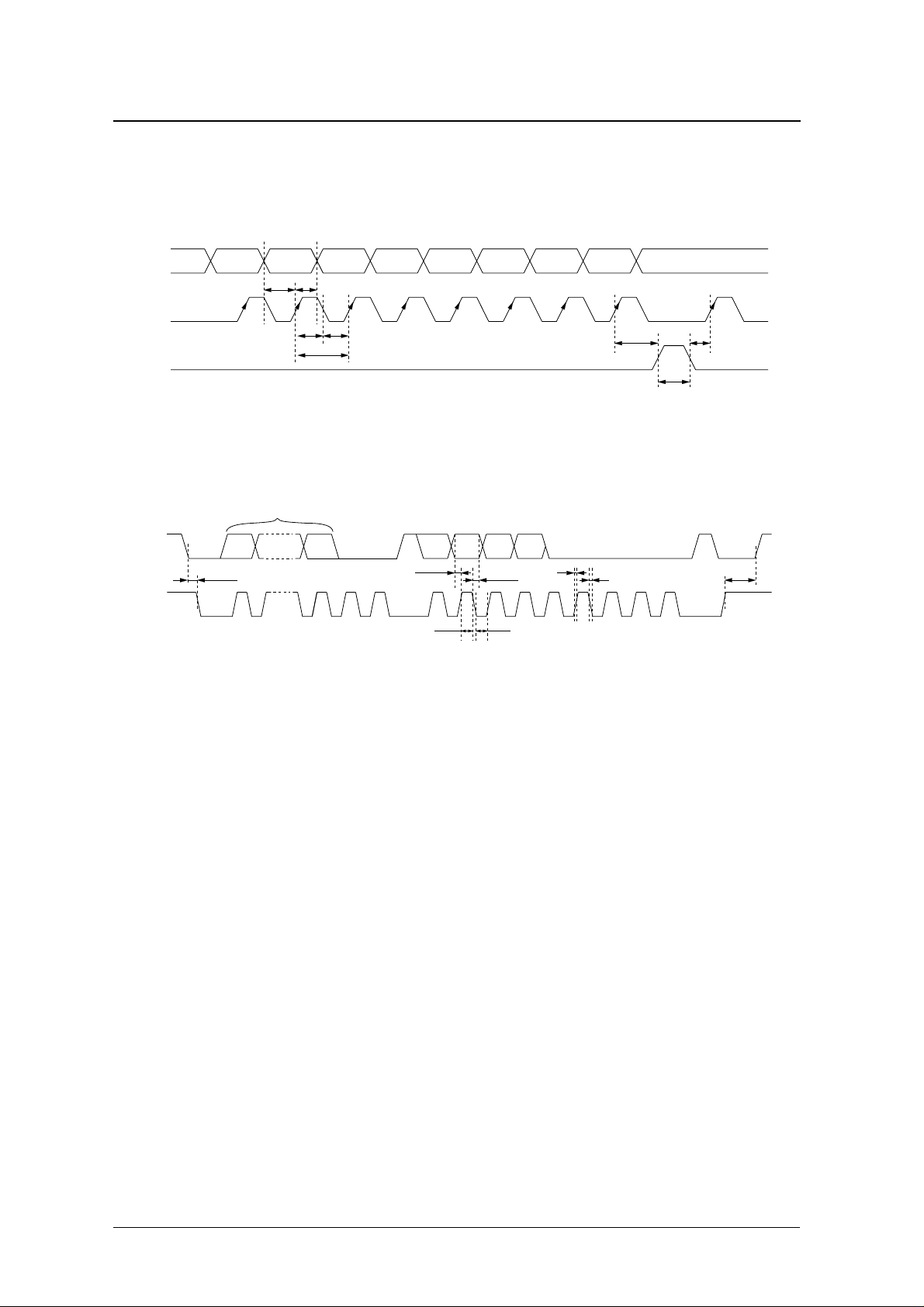
QS7779PM/CM
Serial Interface
Three-wire serial interface (for QS7779PM)
SDA
SCL
STRB
2
I
C serial interface (for QS7779CM)
SDA
SCL
BYP SPRD MUTE PSAVE
t
3t4
t
t
1
2
t
0
2
I C address is {AD6 − AD0} = {1011011}
AD0AD6
t
HD:STA
BYP MUTE
SPRD
t
SU:DAT
t
HIGH
t
HD:DAT
t
LOW
PSAVE
t
5
t
r
t
f
t
7
t
6
t
SU:STO
NIPPON PRECISION CIRCUITS—7
Page 8
FUNCTIONAL DESCRIPTION
Operating Mode
QS7779PM/CM
×
This chip can be set to a desired operating mode by
control pins for the parallel interface (P/S pin sets to
sets to LOW). The control pins or bits configurations
are shown in the following table.
HIGH) or control bits for the serial interface (P/S pin
Mode
No.
11×0 0 LIN RIN Bypass mode
20000QX(LIN) QX(RIN)
30100QX+(LIN) QX+(RIN)
4
5
Note1.
: Don’t care.
Note2. MUTE = 1 when PSAVE = 1
Control Pins/Bits
BYP SPRD MUTE
××
××
1 0 – – Mute mode
1 1 – – Pow er save mode. This function is available with serial interface only
PSAV
E
Operation
(Output signal)
LOUT ROUT
Stereo enhanced and virtual surround mode with low er enhanced
level
Stereo enhanced and virtual surround mode with higher enhanced
level
Mode description
Mode No. Operating description
1 Bypass mode. Outputs the stereo signal as it is input.
Stereo Enhanced and virtual surround mode with low er enhanced level. The Dolby Surround Pro Logic signal (Lt, Rt) input. Available
Surround Effect with two speakers by Qsurround technology. Virtual location of each signal is;
2
The Front signal: Virtually outside of the speakers.
The Rear signal: Virtually behind the listeners.
Stereo Enhanced and virtual surround mode with higher enhanced level. The Dolby Surround Pro Logic signal (Lt, Rt) input. Available
3
Surround Effect with two speakers by Qsurround technology. This mode outputs the signals much more spread sound than Mode 2.
4 Mute mode. No signal at output pins.
5 Power save mode. This function is available with serial interface only.
Description
Center signal output
CIN and COUT are used to emphasize the center signal.
Pin Description
CIN Outputs the doubled signal to ROUT and LOUT always.
COUT Outputs the half level of signal ((RIN+LIN)/2).
How to use CIN and COUT.
■
Connect CIN and COUT with a resistor to make
the center signal emphasized.
■
Input resistance for CIN is 5k Ω. For example, connecting a 5kΩ resistor between CIN and COUT
makes output of (RIN+LIN)/2 to ROUT and
LOUT.
■ Directly connecting CIN and COUT makes ROUT
and LOUT output (RIN+LIN).
NIPPON PRECISION CIRCUITS—8
Page 9
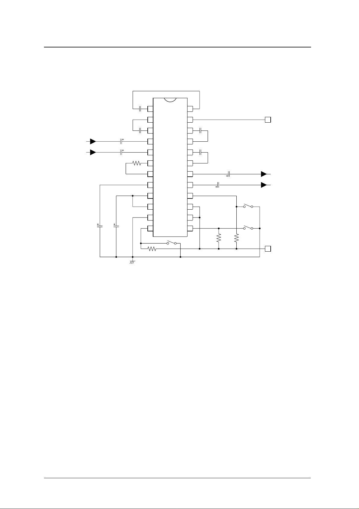
TYPICAL APPLICATION CIRCUIT
QS7779PM/CM with parallel interface
QS7779PM/CM
Signal In
4.7µF
4.7µF
10µF10µF
3300pF
3300pF
1
QXAC3
2
QXAC2
3
QXAC1
4
RIN
5
LIN
3.9k
6
COUT
7
CIN
8
VREFIN
VREFOUT
9
10
VREF
11
GND
SPRD
12 13
(SCL)
QXAC4
VCC
QXBC1
QXBC2
QXBC3
QXBC4
ROUT
LOUT
MUTE
(STRB)
VDD
P/S
BYP
(SDA)
24
5 to 13V
23
0.01µF
22
21
0.01µF
20
19
18
17
16
15
14
4.7µF
4.7µF
Signal Out
47k
5V
NIPPON PRECISION CIRCUITS—9
Page 10
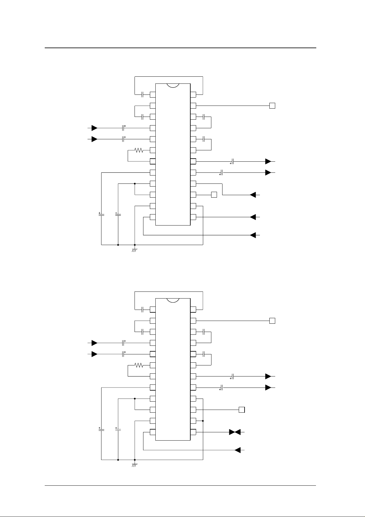
QS7779PM with serial interface
QS7779PM/CM
Signal In
4.7µF
4.7µF
10µF10µF
3300pF
3300pF
1
QXAC3
2
QXAC2
3
QXAC1
4
RIN
5
LIN
3.9k
6
COUT
7
CIN
8
VREFIN
VREFOUT
9
10
VREF
11
GND
SPRD
12 13
(SCL)
QXAC4
VCC
QXBC1
QXBC2
QXBC3
QXBC4
ROUT
LOUT
MUTE
(STRB)
VDD
P/S
BYP
(SDA)
24
5 to 13V
23
0.01µF
22
21
0.01µF
20
19
18
17
16
4.7µF
4.7µF
Signal Out
5V
15
14
STRB
SDA
SCL
QS7779CM with serial interface
3300pF
Signal In
4.7µF
4.7µF
3300pF
3.9k
10µF10µF
1
2
3
4
5
6
7
8
9
10
11
12 13
QXAC3
QXAC2
QXAC1
RIN
LIN
COUT
CIN
VREFIN
VREFOUT
VREF
GND
SPRD
(SCL)
QXAC4
VCC
QXBC1
QXBC2
QXBC3
QXBC4
ROUT
LOUT
MUTE
VDD
P/S
BYP
(SDA)
24
5 to 13V
23
0.01µF
22
21
0.01µF
20
19
18
17
16
4.7µF
4.7µF
Signal Out
5V
15
14
SDA
SCL
NIPPON PRECISION CIRCUITS—10
Page 11

QS7779PM/CM
NIPPON PRECISION CIRCUITS INC. reserves the right to make changes to the products described in this data sheet in order to
improve the design or performance and to supply the best possible products. Nippon Precision Circuits Inc. assumes no responsibility for
the use of any circuits shown in this data sheet, conveys no license under any patent or other rights, and makes no claim that the circuits
are free from patent infringement. Applications for any devices shown in this data sheet are for illustration only and Nippon Precision
Circuits Inc. makes no claim or warranty that such applications will be suitable for the use specified without further testing or modification.
The products described in this data sheet are not intended to use for the apparatus which influence human lives due to the failure or
malfunction of the products. Customers are requested to comply with applicable laws and regulations in effect now and hereinafter,
including compliance with export controls on the distribution or dissemination of the products. Customers shall not export, directly or
indirectly, any products without first obtaining required licenses and approvals from appropriate government agencies.
NIPPON PRECISION CIRCUITS INC.
4-3, Fukuzumi 2-chome
Koto-ku, Tokyo 135-8430, Japan
NIPPON PRECISION CIRCUITS INC.
Telephone: 03-3642-6661
Facsimile: 03-3642-6698
NC9817AE 1999.6
NIPPON PRECISION CIRCUITS—11
 Loading...