

Page 1
PTH 31002
30 Watts, 1.9–2.0 GHz
50-Ohm Power Hybrid
Description
The PTH 31002 is a 50–ohm power hybrid intended for applications
requiring linear power amplification in the PCS frequency range. The
part is designed to operate with 50–ohm source and load impedances
and includes bias circuitry with temperature compensation. The design
is intended to simplify system design and save space with an overall
size of less than one square inch.
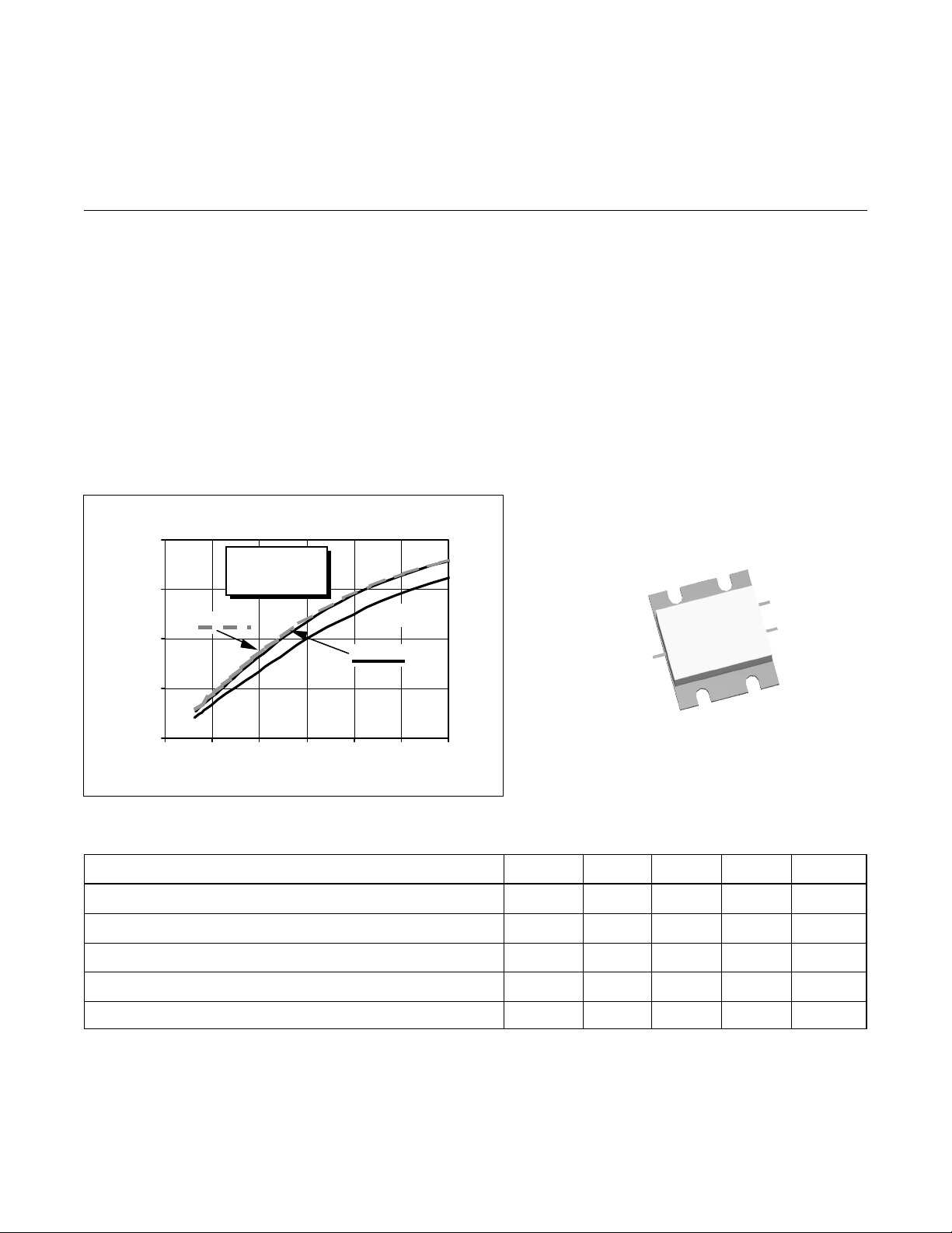
Typical Output Power vs. Input Power
40
VDD = 28.0 V
T
= +25ºC
1.99 GHz
CASE
1.93 GHz
1.96 GHz
30
20
10
Output Power (W)
• Guaranteed Performance at 1.93 to 1.99
GHz, 28 V
- Output Power = 30 Watts (P-1dB) Min
- Power Gain = 12 dB Min
- Efficiency = 30% Min @ P-1dB
• Rugged Hybrid Design
• High Single Stage Gain
• Excellent Linearity
• Input VSWR less than 1.5:1
• Full Gold Metallization
• 100% Lot Traceability
e
31002
A-12345699XX
0
0 0.2 0.4 0.6 0.8 1 1.2
Input Power (W)
Package A
Performance Characteristics
Parameter V
Frequency Range f 1930 — 1990 MHz
Power Gain G
Output Power at 1 dB Compressed P-1dB 30 34 — W
Input VSWR y — 1.25:1 1.5:1 —
Efficiency at P-1dB h 30 35 — %
All published data at T
= 28.0 V, IDQ (Typical) = 550 mA Symbol Min Typ Max Units
DD
12 14 — dB
= 25°C unless otherwise indicated.
CASE
p
e
1
Page 2
PTH 31002
e
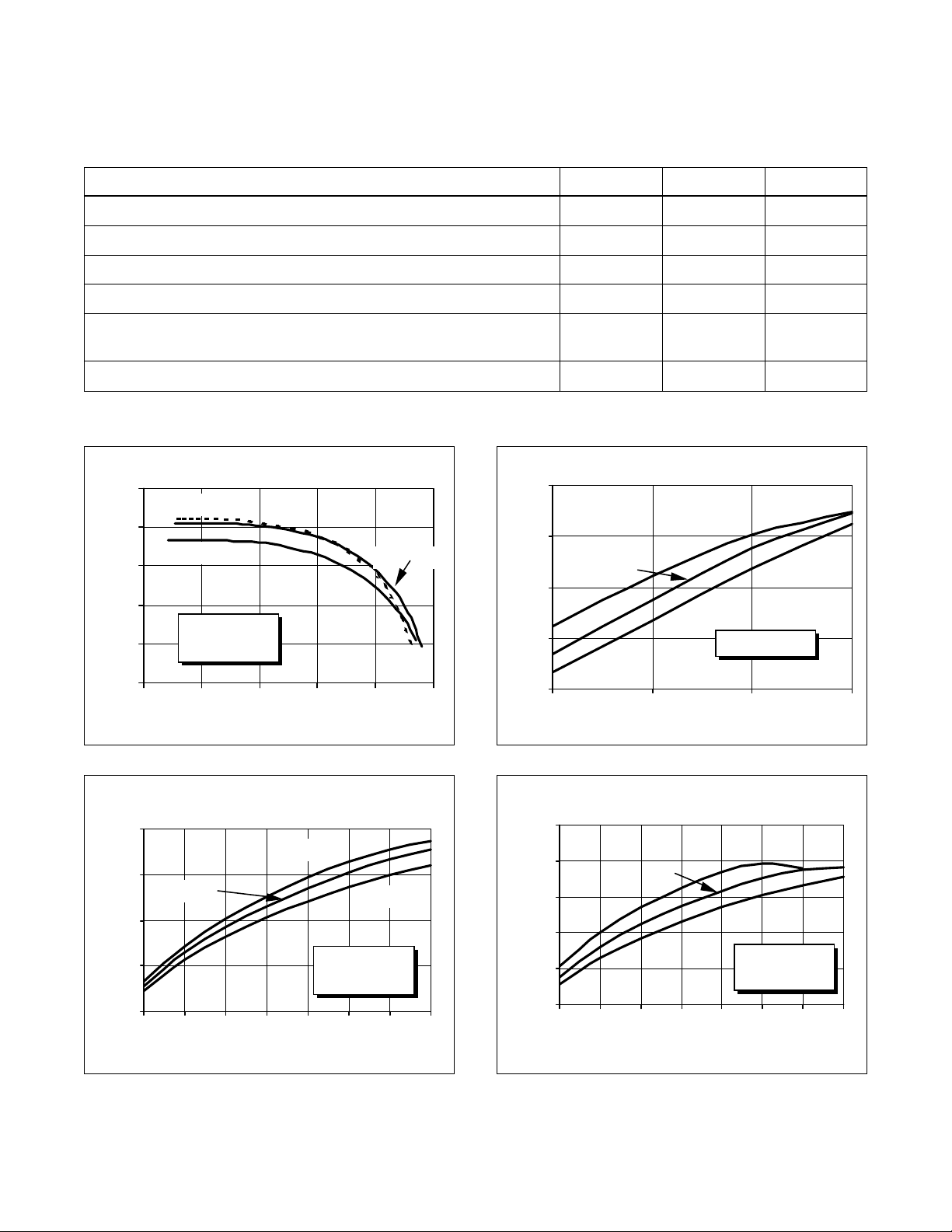
Maximum Ratings
Parameter Symbol Value Unit
Supply Voltage V
Bias Current I
Operating Current — 4.5 A
Operating Temperature T
Total Device Dissipation at T
Above 25°C derate by W/°C
Storage Temperature T
= 25°CP
CASE
DD
DQ
CASE
D
STG
32 Vdc
1000 mA
90 °C
TBD Watts
125 °C
Typical Performance
Power Gain vs. Output Pow e r
18
1.99 GH z
16
1.93 GH z
14
12
Power Gain (dB)
10
VDD = 28. 0 V
T
= +25ºC
CASE
8
0 1020304050
Ou tp u t Power (W)
1.96 GHz
Output Power
35
30
(at P-1dB)
1.96 G H z
25
20
Output Power (W)
1.99 GHz
15
19 22 25 28
Supp ly Voltage (V)
vs. Supply Voltage
1.93 GHz
T
= +25ºC
CASE
Effici en cy vs. Outp u t Power
(at constant vo ltage)
50
1.99 GHz
40
1.96 GHz
30
Efficiency (%)
20
T
V
10
5 10152025303540
Output Power (W)
= +25ºC
CASE
= 28. 0 V
DD
1.93 GHz
Effici en cy vs. Output Power
60
50
40
30
Efficiency (%)
20
10
5 10152025303540
2
(at constant frequency)
25 V
T
f = 1.96 GHz
Ou tp u t Po wer (W)
CASE
22 V
28 V
= +25ºC
Page 3

e
PTH 31002
Gai n and Return Loss vs. Freque ncy
0
-5
-10
Return Loss
-15
-20
T
= +25ºC
Return Loss (dB)
-25
-30
CASE
= 1. 4 W
P
OUT
V
= 28.0 V
DD
1.85 1.9 1.95 2 2.05
Frequ en c y ( GH z )
18
Gain
15
12
9
6
3
0
Inte rm odula ti on Distortion vs. Output Power
-25
-35
-45
-55
IMD (dBc)
VDD = 28. 0 V, T
-65
-75
0 5 10 15 20 25 30 35
f = 1. 96 G Hz, ∆f = 100 K H z
Ou tp u t Po wer (Watts PE P )
3rd Order
CASE
5th Order
7th Order
= 25ºC
Small Signal Gain vs.Supply Voltage
18
1.96 GHz
16
1.93 GH z
14
Gain (dB)
1.99 GHz
T
P
CASE
OUT
= +25ºC
= 1. 4 W
12
Small Signal Gain (dB)
10
12 16 20 24 28
Supply Voltage (V)
IMD3 vs. S upply Voltage
-15
P
= 30 W PEP
OUT
-25
P
= 16 W PEP
OUT
-35
P
= 8 W PEP
OUT
IMD3 (dBc)
-45
P
= 4 W PEP
OUT
-55
19 22 25 28
f = 1.96 GHz, ∆f = 100 K H z
= 25ºC
T
CASE
Supply Voltage (V)
IMD vs. Quiescent Current
-45
-50
-55
-60
IMD (dBc)
-65
-70
-75
490 540 590 640
f = 1.96 GHz, ∆f = 100 KHz
T
= 25ºC, P
CASE
OUT
Quiescen t Curren t ( mA)
5th Order
3rd Order
= 4 W(PEP)
7th Order
Phase Delay vs. Frequency
3.0
2.5
2.0
Phase Delay (ns)
1.5
1.9 1.92 1.94 1.96 1.98 2 2.02
F requency (GHz)
3
T
P
CASE
OUT
= +25ºC
= 1.4 W
Page 4

PTH 31002
e
Phase Linearity vs. Temperature
1.0
0.9
0.8
0.7
0.6
Phase Linearity (deg.)
0.5
-20 0 20 40 60 80 100
Schematic
VDD = 28.0 V
= 1.4 W
P
OUT
Tem p erat u re (ºC)
Quie scent Current vs. Bias Voltage
1200
T
V
CASE
DD
= +25ºC
= 28.0 V
B i a s V o ltage (V )
1000
800
600
400
200
Quiescent Current (mA)
0
9 10111213
4
Page 5

e
Case Outline Specifications
PTH 31002
Package 20237
Ericsson Inc.
Microelectronics
Morgan Hill, CA 95037 USA
1-877-GOLDMOS (465-3667) United States
+46 8 757 4700 International
e-mail: rfpower@ericsson.com
www.ericsson.com\rfpower
5
Specifications subject to change without notice.
LP
© 1998 Ericsson Inc.
EUS/KR 1522-PTH 31002 Uen Rev. A 4-09-01
 Loading...