

Page 1
PTF 10160
85 Watts, 860–960 MHz
GOLDMOS® Field Effect Transistor
Description
The PTF 10160 is an internally matched 85–watt GOLDMOS FET
intended for cellular, GSM, D-AMPS and EDGE applications. It operates with 53% efficiency and 16 dB typical gain. Full gold metallization ensures excellent device lifetime and reliability.
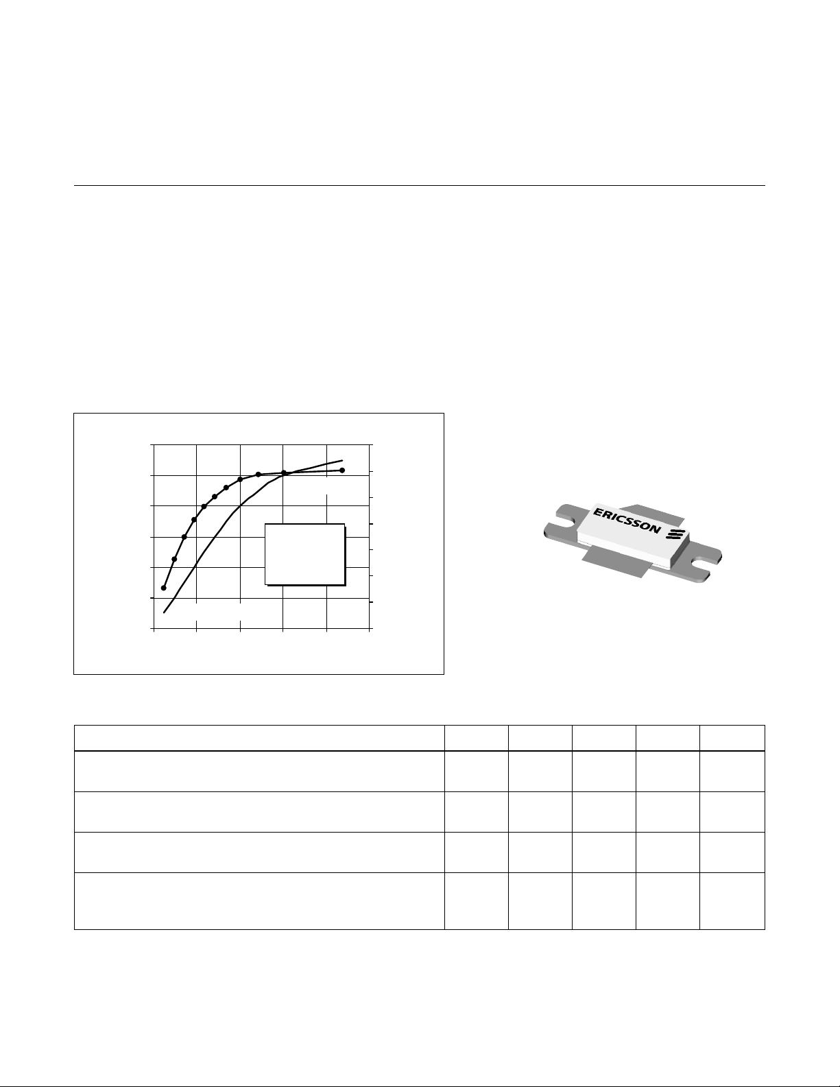
Typical Output Pow er& Efficiency vs. Input Pow er
120
100
80
60
40
20
Output Power (Watts)
Output Power
0
012345
Input Power (Watts)
VDD = 26 V
I
f = 960 MHz
= 700 mA
DQ
Efficiency
70
60
50
40
30
Efficiency (%)
20
10
0
• INTERNALLY MATCHED
• Performance at 960 MHz, 26 Volts
- Output Power = 85 Watts
- Power Gain = 16 dB Typ
- Efficiency = 53% Typ
• Full Gold Metallization
• Silicon Nitride Passivated
• Excellent Thermal Stability
• 100% Lot Traceability
10160
1234560055A
Package 20248
RF Specifications (100% Tested)
Characteristic Symbol Min Typ Max Units
Gain
(V
Power Output at 1 dB Compression
(V
Drain Efficiency
(V
Load Mismatch Tolerance
(V
—all phase angles at frequency of test)
All published data at T
= 26 V, P
DD
= 26 V, IDQ = 700 mA, f = 960 MHz) P-1dB 85 90 — Watts
DD
= 26 V, P
DD
= 26 V, P
DD
= 85 W, IDQ = 700 mA, f = 960 MHz) G
OUT
= 85 W, IDQ = 700 mA, f = 960 MHz) h 50 53 — %
OUT
= 85 W, IDQ = 700 mA, f = 960 MHz Y — — 5:1 —
OUT
= 25°C unless otherwise indicated.
CASE
pe
15 16 — dB
e
1
Page 2
PTF 10160
e
Electrical Characteristics (100% Tested)
Characteristic Conditions Symbol Min Typ Max Units
Drain-Source Breakdown Voltage VGS = 0 V, ID = 25 mA V
(BR)DSS
Drain-Source Leakage Current VDS = 26 V, VGS = 0 V I
Gate Threshold Voltage VDS = 10 V, ID = 75 mA V
Forward Transconductance VDS = 10 V, ID = 3 A g
DSS
GS(th)
fs
65 ——Volts
——1.0 mA
3.0 — 5.0 Volts
— 3.0 — Siemens
Maximum Ratings
Parameter Symbol Value Unit
Drain-Source Voltage V
Gate-Source Voltage V
Operating Junction Temperature T
Total Device Dissipation P
DSS
GS
J
D
Above 25°C derate by 1.18 W/°C
Storage Temperature Range T
Thermal Resistance (T
= 70°C) R
CASE
STG
qJC
65 Vdc
±20 Vdc
200 °C
205 Watts
–40 to +150 °C
0.85 °C/W
Typical Performance
Typical P
, Gain & Efficiency
OUT
vs. Frequency
18
17
16
15
Gain (dB)
14
Gain
13
12
11
10
860 880 900 920 940 960
Frequency (MHz)
Outp ut Power (W)
VDD = 26.0 V
= 700 mA
I
DQ
Efficiency (%)
(at P-1dB)
110
100
90
80
70
60
50
Output Power & Efficiency
Broadband Test Fixture Performance
20
Efficiency (%)
16
Gain
12
Gain (dB)
8
4
860 865 870 875 880 885 890 895 900
VDD = 26 V
= 700 mA
I
DQ
= 85 W
P
OUT
Frequency (MHz)
Return Loss
60
50
40
Efficiency (%)
0
30
- 5
20
-15
10
-20
0
Return Loss (dB)
2
Page 3
e
PTF 10160
Broadband Test Fixture Performance
20
Efficiency (%)
16
Gain
12
Gain (dB)
8
4
920 925 930 935 940 945 950 955 960
VDD = 26 V
= 700 mA
I
DQ
= 85 W
P
OUT
Return Loss
Frequency (MHz)
Output Power vs. Supply Voltage
100
90
80
70
60
50
Output Power (Watts)
40
22 24 26 28 30 32
Supply Voltage (Volts)
IDQ = 700 mA
f = 960 MHz
60
50
40
Efficiency (%)
30
- 5
20
-15
10
-25
0
-35
Return Loss (dB)
17
IDQ = 700 mA
16
IDQ = 400 m
IDQ = 350 mA
15
IDQ = 175 mA
Power Gain (dB)
14
VDD = 28 V
f = 960 MHz
13
1 10 100 1000
Output Power (Watts)
Inter modulation Distortion vs. Output Power
(as measured in a broadband circuit)
-10
Power Gain vs. Output Power
VDD = 26 V, I
-20
-30
-40
IMD (dBc)
-50
-60
= 960 MHz, f2 = 960.1 MHz
f
1
020406080100
Output Power (Watts-PEP)
= 700 mA
DQ
3rd Order
5th
7th
Capacitance vs. V oltage *
300
250
200
150
100
Cds and Cgs (pF)
50
0
0 10203040
C
gs
C
ds
Supply Voltage (Volts)
* This part is internally matched. Measurements of the
finished product will not yield these figures.
VGS = 0 V
f = 1 MHz
C
rss
25
20
15
10
5
0
Crss (pF)
3
Bias Voltage vs. Temper ature
1.03
1.02
1.01
1.00
0.99
0.98
Bias Voltage (V)
0.97
0.96
-20 30 80 130
Voltage normalized to 1.0 V
Series show current (A)
Temp. (°C)
0.86
2.5
4.16
5.8
7.42
9.06
Page 4

PTF 10160
e
Spectrum Due to Modulation (Edge Modulation)
Without correction circuit
200 kHz = -36 dBc
400 kHz = -57 dBc
600 kHz = -70 dBc
4
Page 5

e
Impedance Data
PTF 10160
VDD = 26 V, P
= 85 W, IDQ = 700 mA
OUT
D
Z Source Z Load
G
S
Frequency Z Source W Z Load W
MHz R jX R jX
860 2.1 -1.5 2.6 1.1
880 2.6 -1.6 2.6 1.3
900 3 -1.7 2.6 1.5
920 4.1 -1.7 2.4 1.5
940 6.3 -1.5 2.3 1.65
960 7.1 1.5 2.2 1.8
Test Circuit
Z0 = 50 W
Test Circuit Schematic for f = 921 to 960 MHz
DUT PTF 10160 LDMOS Transistor
l1, l9 0.037 l Microstrip 50 W
l2 0.120 l Microstrip 50 W
l3 0.080 l Microstrip 50 W
l4 0.187 l Microstrip 9.29 W
l5 0.204 l Microstrip 6.98 W
l6 0.250 l Microstrip 77.9 W
l7 0.031 l Microstrip 50 W
l8 0.157 l Microstrip 50 W
l1, l9 0.037 l Microstrip 50 W
C1, C3, C4, C8 100 B Capacitor, 36 pF
C2 100 B Capacitor, 2.7 pF
C5 Digi-Key P4525-ND Capacitor, 0.1 µF, 50 V
C6 Digi-Key P5182-ND Capacitor, 100 µF, 50 V
C7 ATC 100 B Capacitor, 3.3 pF
J1, J2 SMA Panel Mount Female Connector
R1, R2, R3 220 W Resistor, Digi-Key 1K QBK
Circuit Board .031" Thickness,
AlliedSignal, G200, 2 oz. copper
5
e
r
= 4.0,
Page 6

PTF 10160
Components Layout (not to scale)
e
10160
Artwork (not to scale)
ERICSSON
10160_A OUTPUT
6
Page 7

e
Case Outline Specifications
PTF 10160
Package 20248
Primary dimensions are inches; alternate dimensions are mm.
Ericsson Inc.
Microelectronics
Morgan Hill, CA 95037 USA
1-877-GOLDMOS (465-3667) United States
+46 8 757 4700 International
e-mail: rfpower@ericsson.com
www.ericsson.com/rfpower
7
Specifications subject to change without notice.
L3
© 1999, 2000, 2001 Ericsson Inc.
EUS/KR 1522-PTF 10160 Uen Rev. A 12-03-00
 Loading...