

Page 1
PTF 10139
60 Watts, 860-960 MHz
GOLDMOS® Field Effect Transistor
Description
The PTF 10139 is a GOLDMOS FET intended for amplifier applications to 860-960 MHz. This 60–watt device operates at 55% efficiency with 12.5 dB typical gain. Nitride surface passivation and full
gold metallization ensure excellent device lifetime and reliability.
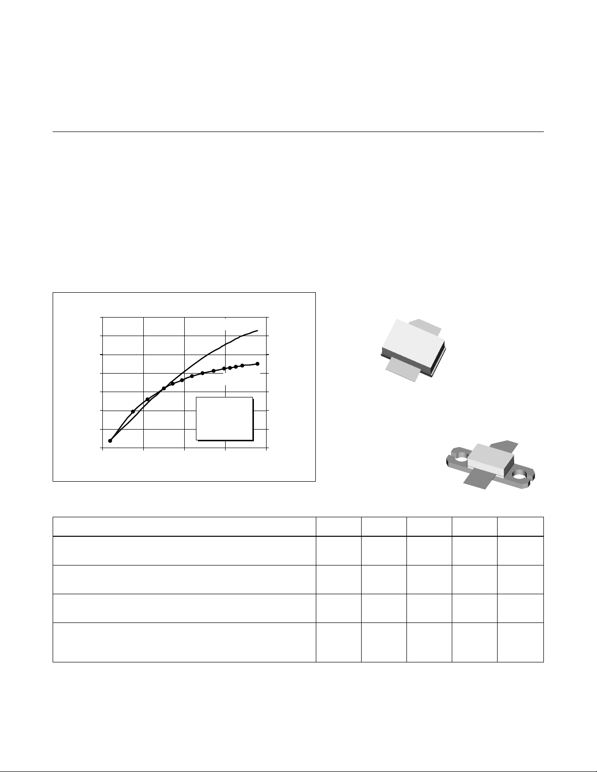
Typical Output Pow er & Efficiency vs. Input Power
70
60
50
40
30
20
10
Output Power (Watts)
0
01234
Input Power (Wa tts)
Output Power
Efficiency
VDD = 28 V
I
= 500 mA
DQ
f = 960 MHz
80
70
60
50
40
30
20
10
Drain Efficiency (%) X
• Performance at 960 MHz, 28 Volts
- Output Power = 60 Watts Min
- Power Gain = 12.5 dB Typ
- Efficiency = 55% Typ
• Full Gold Metallization
• Silicon Nitride Passivated
• Excellent Thermal Stability
• Back Side Common Source
• 100% Lot Traceability
• Available in Package 20256 as PTF 10138
e
10139
A-1234561199
Also available in
Package
20256
Package
e
10138
A-1234562700
20251
RF Specifications (100% Tested)
Characteristic Symbol Min Typ Max Units
Common Source Power Gain
(V
Power Output at 1 dB Compression
(V
Drain Efficiency
(V
Load Mismatch Tolerance
(V
all phase angles at frequency of test)
All published data at T
= 28 V, P
DD
= 28 V, IDQ = 500 mA, f = 960 MHz) P-1dB 60 — — Watts
DD
= 28 V, P
DD
= 28 V, P
DD
= 60 W, IDQ = 500 mA, f = 960 MHz) G
OUT
= 60 W, IDQ = 500 mA, f = 960 MHz) h 50 55 — %
OUT
= 60 W, IDQ = 500 mA, f = 960 MHz— Y — — 10:1 —
OUT
= 25°C unless otherwise indicated.
CASE
ps
11.5 12.5 — dB
e
1
Page 2
PTF 10139
e
Electrical Characteristics (100% Tested)
Characteristic Conditions Symbol Min Typ Max Units
Drain-Source Breakdown Voltage VGS = 0 V, ID = 25 mA V
(BR)DSS
Drain-Source Leakage Current VDS = 28 V, VGS = 0 V I
Gate-Source Leakage Current VGS = 20 V, VDS = 0 V I
Gate Threshold Voltage VDS = 10 V, ID = 75 mA V
Forward Transconductance VDS = 10 V, ID = 3 A g
DSS
GSS
GS(th)
fs
65 ——Volts
——1.0 mA
——1 mA
3.0 — 5.0 Volts
— 2.8 — Siemens
Maximum Ratings
Parameter Symbol Value Unit
Drain-Source Voltage V
Gate-Source Voltage V
Drain Current - Continuous I
Operating Junction Temperature T
Total Device Dissipation P
DS
GS
D
J
D
Above 25°C derate by 1.11 W/°C
Storage Temperature Range T
Thermal Resistance (T
= 70°C) R
CASE
STG
qJC
65 Vdc
±20 Vdc
7 Adc
200 °C
194 Watts
-65 to 150 °C
0.9 °C/W
Typical Performance
Typical P
14
Gain (dB)
13
VDD = 28 V
12
I
DQ
Gain
11
10
9
840 860 880 900 920 940 960
, Gain & Efficiency
OUT
vs. Frequency
= 500 mA
Frequency (MHz)
Outp ut P ower (W)
(at P-1dB)
Efficiency (%)
90
80
70
60
50
Output Power & Efficiency
40
Broadband Test Fixture Perfor mance
14
13
12
11
Gain (dB)
Gain
10
9
8
920 930 940 950 960
Return Loss (dB)
Frequency (MHz)
Efficiency (%)
VDD = 28 V
= 500 mA
I
DQ
= 60 W
P
OUT
60
50
40
30
- 5
20
-15
10
-25
0
EfficiencyReturn Loss
2
Page 3

e
PTF 10139
Power Gain vs. Output Power
14
IDQ = 500 mA
13
IDQ = 320 mA
12
IDQ = 225 mA
Power Gain (dB)
11
VDD = 28 V
f = 960 MHz
10
0 1 100
Output Power (Watts)
Inter modulation Distort ion vs. O utput Pow er
(as measured in a broadband circuit)
-20
VDD = 28 V
= 500 mA
I
DQ
-30
= 959.90 MHz
f
1
= 960.00 MHz
f
2
-40
IMD (dBc)
-50
-60
0 10203040506070
Output Power (Watts-PEP)
3rd Order
5th
7th
Output Power vs. Supply Voltage
75
70
65
60
55
Output Power (Watts)
50
24 26 28 30 32
IDQ = 500 mA
f = 960 MHz
Supply Voltage (Volts)
Capacitance vs. Supply Voltage
140
120
100
Cds & Cgs (pF)
80
60
40
20
C
gs
VGS = 0 V
f = 1 MHz
C
ds
C
0
0 10203040
rss
Supply Voltage (Volts)
24
20
16
12
8
4
0
Crss (pF)
Bias Voltage vs. C ase Temperature
1.04
1.03
1.02
1.01
1.00
0.99
0.98
0.97
0.96
Gate-Source Voltage (V)
0.95
-20 30 80 130
Voltage normalized to 1.0 V
Series show current (A)
Case Temperature (°C)
3
0.4
1.364
2.328
3.292
4.256
5.22
Page 4

PTF 10139
Impedance Data
VDD = 28 V, P
= 60 W, IDQ = 500 mA
OUT
D
Z Source Z Load
e
5
.
0
Z0 = 10 W
4
.
5
0
.
0
0
5
4
.
0
3
.
0
G
2
.
->
0
-
-
R
O
S
Frequency Z Source W Z Load W
MHz R jX R jX
850 0.60 0.40 2.35 0.74
860 0.56 0.56 2.20 0.72
900 0.55 0.80 1.80 0.95
920 0.58 0.90 1.80 1.10
960 0.65 1.10 1.80 1.30
T
A
R
E
Z Source
N
E
G
D
R
960 MHz
A
W
O
T
S
H
T
G
N
E
L
E
V
A
850 MHz
W
-
-
D
A
O
L
D
R
A
W
O
T
S
H
T
G
N
E
L
E
V
A
Z Load
1
.
0
0
.
0
0.1
1
.
0
960 MHz
850 MHz
0.2
Typical Scattering Parameters
(VDS = 28 V, ID = 1.5 A)
f S11 S21 S12 S22
(MHz) Mag Ang Mag Ang Mag Ang Mag Ang
300 0.941 -175 2.70 36.8 0.028 -82.1 0.993 -175
350 0.949 -176 2.09 32.7 0.022 -82.7 0.990 -176
400 0.958 -178 1.71 28.3 0.017 -83.6 0.991 -178
450 0.968 -179 1.40 24.7 0.013 -82.9 0.994 -179
500 0.975 -179 1.20 22.3 0.009 -83.4 0.998 -179
550 0.973 180 1.03 18.0 0.006 -78.3 0.996 -180
600 0.974 179 0.892 14.6 0.003 -71.0 0.996 180
650 0.982 178 0.788 10.5 0.001 -19.9 0.996 179
700 0.985 177 0.671 6.38 0.003 44.0 0.997 178
750 0.981 177 0.576 3.31 0.004 68.8 0.999 178
800 0.979 176 0.489 0.641 0.007 71.9 0.996 177
850 0.986 175 0.425 0.228 0.008 70.1 0.990 176
900 0.984 175 0.378 0.643 0.010 76.6 0.992 176
950 0.986 174 0.342 -0.107 0.011 79.0 0.994 176
1000 0.992 173 0.316 -0.098 0.014 81.0 0.996 175
1050 0.990 173 0.294 -0.827 0.016 80.6 0.989 175
1100 0.983 172 0.264 -1.69 0.018 78.5 0.985 174
1150 0.984 171 0.245 -2.59 0.020 76.4 0.990 173
1200 0.993 171 0.228 -3.43 0.022 76.2 0.993 173
1250 0.991 171 0.211 -3.76 0.023 76.6 0.987 173
1300 0.986 170 0.192 -4.91 0.025 76.4 0.986 173
1350 0.982 169 0.179 -4.94 0.028 73.3 0.988 172
1400 0.990 169 0.173 -5.51 0.030 69.4 0.986 172
1450 0.991 169 0.159 -5.77 0.029 67.2 0.990 171
1500 0.986 168 0.146 -5.99 0.030 66.3 0.985 171
0.3
0.5
0.4
4
Page 5

e
Test Circuit
Test Circuit Schematic for f = 960 MHz
PTF 10139
D.U.T. PTF 10139
l1 0.190 l 960 MHz Microstrip 50 W
l2 0.075 l 960 MHz Microstrip 15.7 W
l3 0.141 l 960 MHz Microstrip 5.2 W
l4 0.017 l 960 MHz Microstrip 5.2 W
l4 0.122 l 960 MHz Microstrip 8.3 W
l4 0.191 l 960 MHz Microstrip 8.3 W
l5 0.015 l 960 MHz Microstrip 50 W
l6 0.225 l 960 MHz Microstrip 50 W
C1, C8 Capacitor, 3.0 pF 100 B 3r0
C2, C3, C5, C9 Capacitor, 36 pF 100 B 360
C4 Capacitor, 2.0 pF 100 B 2r0
C6 Capacitor, 0.1 mF, 50 V Digi-Key P4525-ND
C7 Capacitor, 100 mF, 50 V Digi-Key P5182-ND
J1, J2 Connector, SMA, Female, Panel Mount
Ericsson, #Rpm 513 412/53
L1 4 Turns, 22 Awg, .120 I.D.
R1, R2, R3 Resistor, 220ohm, 1/4w Digi-key 220qbk-no
Circuit Board .031” thick,
Signal
e
= 4.0, 2 Oz Copper, G200,Allied
r
Assembly Diagram (not to scale)
5
Page 6

PTF 10139
Artwork (not to scale)
e
10138_B INPUT 10138_A OUTP UT
Ericsson Inc.
Microelectronics
Morgan Hill, CA 95037 USA
1-877-GOLDMOS (465-3667) United States
+46 8 757 4700 International
e-mail: rfpower@ericsson.com
www.ericsson.com/rfpower
6
Specifications subject to change without notice.
L3
© 1999, 2000 Ericsson Inc.
EUS/KR 1522-PTF 10139 Uen Rev . A2 12-03-00
 Loading...