

Page 1
PTF 10107
5 Watts, 2.0 GHz
GOLDMOS® Field Effect Transistor
Description
The PTF 10107 is a 5–watt GOLDMOS FET intended for large signal
applications from 1.0 to 2.0 GHz. It operates at 40% efficiency with
11 dB gain. Nitride surface passivation and full gold metallization
ensure excellent device lifetime and reliability.
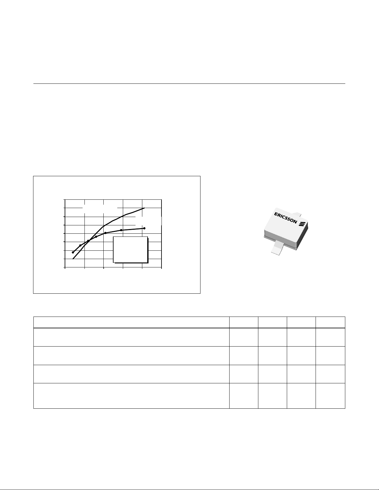
Typical Output Pow e r & Efficie ncy
vs. Input Power
8
7
6
5
4
3
2
1
Output Power (Watts)
0
0.0 0.1 0.2 0.3 0.4 0.5
Output Power
VDD = 26 V
I
= 70 mA
DQ
f = 2.0 GHz
Inp u t Power (Watts)
Eff iciency
100
80
60
40
20
0
Efficiency (%) X
• Guaranteed Performance at 1.99 GHz, 26 V
- Output Power = 5 Watts Min
- Power Gain = 11 dB Min
• Full Gold Metallization
• Silicon Nitride Passivated
• Back Side Common Source
• Excellent Thermal Stability
• 100% Lot Traceability
10107
A-1234569845
Package 20244
RF Specifications (100% T ested)
Characteristic Symbol Min Typ Max Units
Gain
(V
Power Output at 1 dB Compression
(V
Drain Efficiency
(V
Load Mismatch Tolerance
(V
—all phase angles at frequency of test)
All published data at T
= 26 V , P
DD
= 26 V , IDQ = 70 mA, f = 1.99 GHz) P-1dB 5 6.5 — Watts
DD
= 26 V , P
DD
= 26 V , P
DD
= 1 W, IDQ = 70 mA, f = 1.93, 1.99 GHz) G
OUT
= 5 W, IDQ = 70 mA, f = 1.99 GHz) h
OUT
= 5 W, IDQ = 70 mA, f = 1.99 GHz Y — — 10:1 —
OUT
= 25°C unless otherwise indicated.
CASE
ps
D
11 — — dB
40 — — %
e
1
Page 2
PTF 10107
G
-
e
Electrical Characteristics (100% Tested)
Characteristic Conditions Symbol Min T yp Max Units
Drain-Source Breakdown Voltage VGS = 0 V , ID = 20 mA V
(BR)DSS
Zero Gate Voltage Drain Current VDS = 26 V , VGS = 0 V I
Gate Threshold Voltage VDS = 10 V , ID = 75 mA V
Forward Transconductance VDS = 10 V , ID = 2 A g
DSS
GS(th)
fs
65 ——Volts
——1.0 mA
3.0 — 5.0 Volts
— 0.8 — Siemens
Maximum Ratings
Parameter Symbol Value Unit
Drain-Source Voltage V
Gate-Source Voltage V
Operating Junction T emperature T
T otal Device Dissipation at P
DSS
GS
J
D
Above 25°C derate by 0.22 W/°C
Storage T emperature Range T
Thermal Resistance (T
= 70°C) R
CASE
STG
qJC
65 Vdc
±20 Vdc
200 °C
39 Watts
–40 to +150 °C
4.5 °C/W
Typical Performance
P
, Gain & Efficiency
OUT
15
13
ain (dB)
11
VDD = 26 V
9
I
= 70 mA
DQ
7
Gain & Output Power x
Output Power
5
1750 1800 1850 1900 1950 2000 2050
(at P-1dB)
Efficiency (%)
F requency (MHz)
vs. Freque ncy
65
55
45
35
25
15
Efficiency
Broadba nd Test Fixture Performa nce
14
Gain (dB)
12
= 70 mA
DQ
= 4 W
OUT
Efficiency (%)
10
8
Gain
6
4
2
1925 1950 1975 2000
Return Loss (dB)
VCC = 26 V
I
P
Freque ncy (MHz)
60
50
40
- 5
30
-15
20
10
-25
0
35
Efficiency
Return Loss
2
Page 3

e
CgsCdsC
C
I
I
=
I
PTF 10107
Output Powe r vs. Supply Vol ta ge
10
8
6
4
2
Output Power (Watts)
0
22 24 26 28 30
IDQ = 70 mA
f = 2.0 GHz
Supply Voltage (Volts)
Power Gain vs. Output Power
14
= 70 mA
DQ
40 mA
DQ
= 20 mA
DQ
VDD = 26 V
f = 2.0 GHz
0.1 1.0 10.0
Outp ut Po wer (Watts)
Power Gain (dB)
13
12
11
10
9
8
Intermodul ation Distortion vs. Output Power
0
VDD = 26 V
-10
I
= 70 mA
DQ
-20
-30
-40
IMD (dBc)
-50
-60
-70
= 1999.9 MHz
f
1
f
= 2000.0 MHz
2
01234567
IM3
IM5
IM7
Outp u t Po wer (Watts-PEP)
Capa cita nce vs. Suppl y Vol ta ge
18
15
gs
0 10203040
Cds and Cgs (pF)
12
x
9
6
3
0
Supply Voltage (Volts)
VGS = 0 V
f = 1 MHz
rss
6
5
4
3
2
1
0
Crss (pF)
Bias Voltage vs. Temperature
1.03
1.02
1.01
1
0.99
0.98
Bias Voltage (V)
0.97
0.96
-20 30 80 130
Voltage normalized to 1.0 V
Series show current (A)
0.05
0.145
0.24
0.335
0.43
0.525
Temp. (°C)
3
Page 4

PTF 10107
Impedance Data
e
VDD = 26 V , P
= 5 W, IDQ = 70 mA
OUT
D
Z Source Z Load
G
S
Frequency Z Source W Z Load W
GHz R jX R jX
1.75 3.2 -1.7 6.20 2.4
1.80 3.4 -2.0 6.80 1.7
1.85 3.4 -2.4 7.10 0.9
1.90 3.7 -3.1 7.05 0.5
1.95 3.5 -3.8 7.00 0.0
2.00 3.0 -4.1 6.70 -0.4
2.05 2.7 -4.6 6.00 -0.8
Z0 = 50 W
Typical Scattering Parameters
(VDS = 26 V, ID = 300 mA)
f S11 S21 S12 S22
(MHz) Mag Ang Mag Ang Mag Ang Mag Ang
100 0.874 -58 24.1 137 0.009 46 0.770 -35
200 0.837 -70 21.8 129 0.010 37 0.737 -42
300 0.844 -100 17.5 106 0.012 21 0.710 -62
400 0.850 -118 14.1 89 0.013 9 0.709 -77
500 0.858 -130 11.5 77 0.012 -1 0.723 -88
600 0.864 -139 9.44 66 0.011 -8 0.749 -98
700 0.868 -146 7.86 56 0.009 -13 0.767 -108
800 0.870 -153 6.61 48 0.008 -15 0.782 -116
900 0.879 -158 5.65 40 0.006 -13 0.801 -123
1000 0.887 -162 4.86 33 0.004 -2 0.815 -130
1100 0.898 -167 4.24 26 0.004 19 0.837 -136
1200 0.905 -171 3.73 20 0.004 48 0.854 -141
1300 0.911 -174 3.30 14 0.005 66 0.870 -147
1400 0.914 -178 2.92 8 0.006 74 0.882 -152
1500 0.916 179 2.61 2 0.008 77 0.892 -156
1600 0.918 176 2.35 -3 0.009 79 0.898 -160
1700 0.923 173 2.14 -8 0.011 79 0.907 -164
1800 0.928 171 1.95 -13 0.013 78 0.914 -168
1900 0.933 168 1.79 -18 0.015 76 0.920 -172
2000 0.937 165 1.65 -23 0.017 74 0.925 -176
2100 0.935 162 1.53 -28 0.018 71 0.929 -179
2200 0.934 159 1.43 -33 0.020 68 0.934 178
4
Page 5

e
Test Circuit
Block Diagram for f = 1.96 GHz
DUT PTF 10107 LDMOS RF FET
l1 0.303 l 1.99 GHz Microstrip 50 W
l2 0.146 l 1.99 GHz Microstrip 11.6 W
l3 0.076 l 1.99 GHz Microstrip 17.7 W
l4 0.072 l 1.99 GHz Microstrip 13.5 W
l5 0.060 l 1.99 GHz Microstrip 17.7 W
l6 0.352 l 1.99 GHz Microstrip 50 W
PTF 10107
C1 Capacitor, 0.1 µF Digi-Key P4525-ND
C2, C3, C6, C9 Capacitor, 33 pF ATC 100 B
C4, C10 Capacitor, 0.5 pF ATC 100 B
C5 Capacitor, 1.1 pF ATC 100 B
C7 Capacitor , 0.1 µF 50 V Digi-Key
C8 Capacitor , 100 µF, 50 V Digi-Key P5182-ND
J1, J2 Connector, SMA, Female, Panel Mount
L1 Chip Inductor, 2.7 µH Digi-Key LL2012-F2N7K
L2 3 Turns, 20 A WG, .120 I. D. N/A
R1, R2 Resistor, 220 ohm, 1/4W Digi-Key QBK-ND
Circuit Board 0.031" Thick,
e
= 4.0, 2 0z copper, G200 AlliedSignal
r
5
Page 6

PTF 10107
Artwork (not to scale)
e
Ericsson Inc.
Microelectronics
Morgan Hill, CA 95037 USA
1-877-GOLDMOS (465-3667) United States
+46 8 757 4700 International
e-mail: rfpower@ericsson.com
www.ericsson.com/rfpower
6
Specifications subject to change without notice.
L3
© 1998, 1999, 2000, 2001 Ericsson Inc.
EUS/KR 1522-PTF 10107 Uen Rev. B 01-04-01
 Loading...