

Page 1
e
)
165 Watts, 860–900 MHz
LDMOS Field Effect Transistor
Description
The 10100 is an internally matched common source N-channel
enhancement-mode lateral MOSFET intended for large signal amplifier
applications from 860 to 900 MHz. It is rated at 165 watts power output.
Nitride surface passivation and gold metallization ensure excellent
device lifetime and reliability.
PTF 10100
•
INTERNALLY MA TCHED
• Performance at 894 MHz, 28 Volts
- Output Power = 165 Watts
- Power Gain = 13.0 dB Typ
- Drain Efficiency = 50% T yp
• Full Gold Metallization
• Silicon Nitride Passivated
• Back Side Common Source
• 100% lot traceability
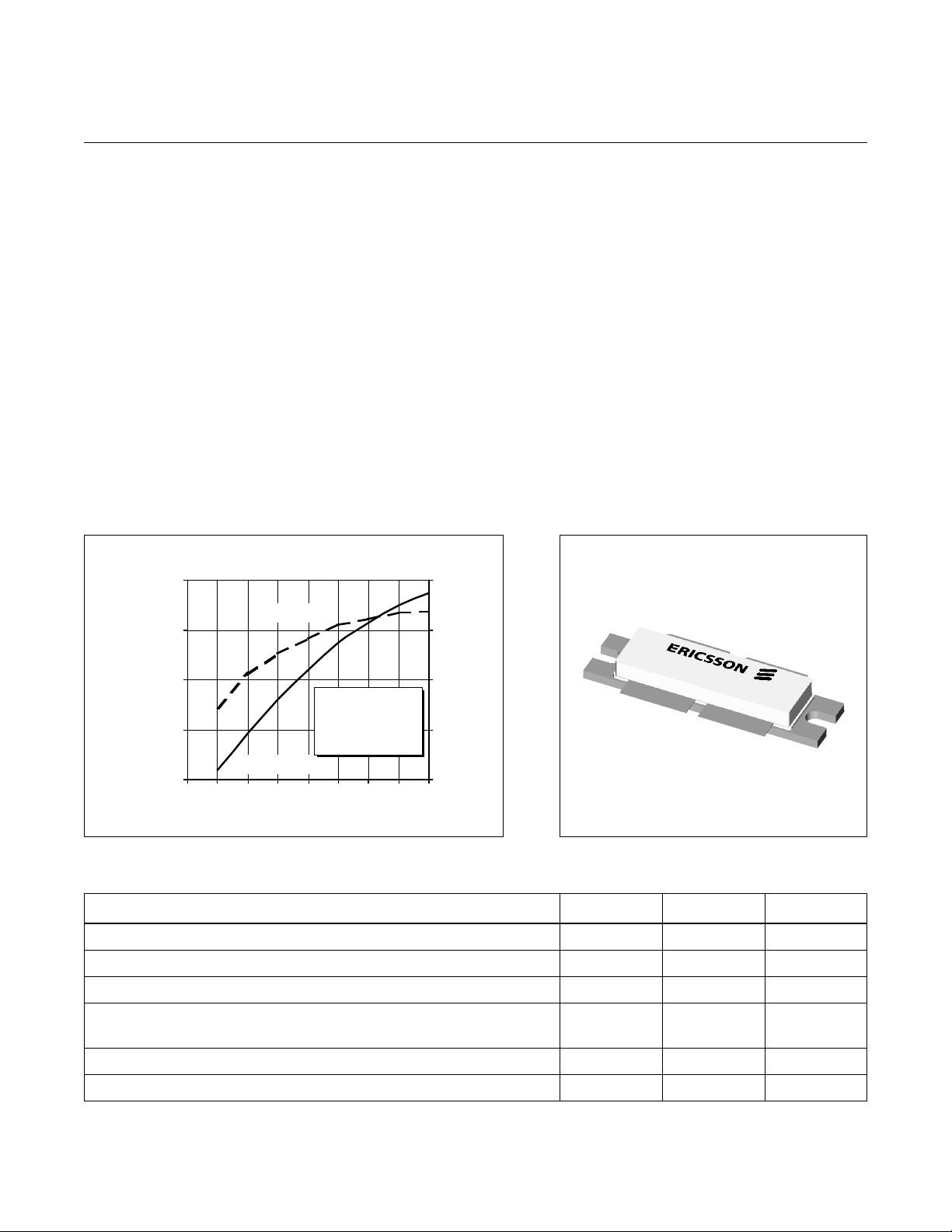
Typical Output Pow er & Efficiency vs. Input Power
180
Efficiency
140
100
VDD = 28.0 V
= 1.8 A Tota l
I
60
Output Power (Watts)
Output Power
20
012345678
Input Power (Watts)
DQ
f = 880 MHz
60
45
30
Efficiency (%
15
0
10100
A-1234569917
Package 20250
Maximum Ratings
Parameter Symbol Value Unit
Drain-Source Voltage
Gate-Source Voltage
Operating Junction T emperature T
T otal Device Dissipation at T
Above 25°C derate by 2.85 W/°C
Storage T emperature Range T
Thermal Resistance (T
(1)
per side
(1)
(1)
flange
= 25°C P
flange
= 70°C) R
V
DSS
V
STG
GS
J
D
qJC
65 Vdc
±20 Vdc
200 °C
500 Watts
–40 to +150 °C
0.35 °C/W
1
Page 2
PTF 10100
y
s
y
e
Electrical Characteristics (per side) (100% T ested)
Characteristic Conditions Symbol Min T yp Max Units
Drain-Source Breakdown Voltage VGS = 0 V , ID = 5 mA V
(BR)DSS
Drain-Source Leakage Current VDS = 28 V , VGS = 0 V I
Gate Threshold Voltage VDS = 10 V , ID = 75 mA V
Forward Transconductance VDS = 10 V , ID = 3 A g
DSS
GS(th)
fs
65 — — Volts
— — 1.0 mA
— 4.3 — Volts
— 2.5 — Siemens
RF Specifications (100% T ested)
Characteristic Symbol Min T yp Max Units
Gain
(V
Power Output at 1 dB Compression
(V
Drain Efficiency
(V
Load Mismatch Tolerance
(V
f = 893.9, 894 MHz—all phase angles at frequency of test)
= 28 V , P
DD
= 28 V , ICQ = 1.8 A Total, f = 880 MHz) P-1dB 165 180 — Watts
DD
= 28 V , P
DD
= 28 V , P
DD
= 165 W, IDQ = 1.8 A Total, f = 894 MHz) G
OUT
= 165 W, IDQ = 1.8 A Total, f = 894 MHz) h 45 50 — %
OUT
= 165 W(PEP), IDQ = 1.8 A Total, Y — — 10:1 —
OUT
ps
12.0 13.0 — dB
Typical Performance
Typical P
18
16
14
Gain
Gain (dB)
12
10
865 870 875 880 885 890 895
(at P- 1dB) , Gain vs. Frequency
OUT
Out pu t Power (W)
VDD = 28 V
= 1.8 A Total
I
DQ
Efficiency (%)
Frequency (MHz)
225
175
125
75
Output Power & Efficienc
25
Broadband Test Fixture Performance
16
Efficiency (%)
14
Gain
12
Gain (dB)
10
8
865 870 875 880 885 890 895
VDD = 28 V
= 1.8 A Tota l
I
DQ
= 165 W
P
OUT
Frequency (MHz)
Return
Loss (dB)
60
50
40
30
- 5
20
-10
10
-15
-20
0
-25
Efficienc
Return Los
2
Page 3

e
Typical Performance
PTF 10100
Output Power vs. Supply Volt age
200
180
160
140
120
100
80
Output Power (Watts)
60
40
18 20 22 24 26 28 30
IDQ =1.8 A Tota l
f = 894 MHz
Supply Voltage (Volts)
Capacitance vs. Supply Volt age
600
500
400
300
200
Cds & Cgs (pF)
100
0
0 10203040
C
gs
C
ds
Supply Voltage (Volts)
Inter modulation Distortion vs. Output Power
-10
VDD = 28 V
-20
-30
-40
IMD (dBc)
-50
-60
VGS = 0 V
f = 1 MHz
= 1.8 A Tota l
I
CQ
= 880.0 MHz
f
1
= 880.1 MHz
f
2
30 50 70 90 110 130 150 170
3rd order
Output Power (Watts-PEP)
(per side)
C
rss
95
85
75
65
55
45
35
25
15
5
*
Crss (pF)
*This part is internally matched. Measurements of the finished
product will not yield these figures.
3
Page 4

PTF 10100
W
Impedance Data
VDD = 28 V , IDQ = 1.8 A Total, P
Z Source Z Load
Frequency Z Source W Z Load W
MHz R jX R jX
860 2 .3 1.6 1.60 -1.1
870 1 .9 0.8 1.70 -1.7
880 1 .8 0.3 1.90 -2.1
890 1 .7 0.1 1.95 -1.8
900 1.6 -0.2 1.80 -1.5
OUT
G
G
= 165 W
D
S
D
S
H
T
G
N
E
L
E
V
A
W
-
G
D
R
A
W
O
T
e
>
-
-
-
R
O
T
RA
E
N
E
-
D
900 MHz
A
O
860 MHz
L
D
R
A
W
O
T
S
H
T
G
N
E
L
E
V
A
2
.
0
1
.
0
Z Source
860 MHz
0
.
0
Z Load
1
.
0
Z0 = 50 W
0.1
9
0
0
MHz
Typical Scattering Parameters
(VDS = 28 V, ID = 2 A per side)
f S11 S21 S12 S22
(MHz) Mag Ang Mag Ang Mag Ang Mag Ang
300 0.980 -178 0.996 15.6 0.010 -85.2 0.994 -177
350 0.982 -179 0.773 12.8 0.008 -85.3 0.993 -177
400 0.983 -180 0.641 9.48 0.006 -85.7 0.992 -178
450 0.989 179 0.545 7.19 0.005 -85.3 0.996 -179
500 0.989 179 0.489 5.48 0.003 -93.7 0.999 -179
550 0.987 179 0.449 2.11 0.002 -74.5 0.995 -179
600 0.983 178 0.425 -0.90 0.002 -64.9 0.996 -179
650 0.982 177 0.414 -4.52 0.001 -68.5 0.998 -180
700 0.980 176 0.405 -10.2 0.001 -55.1 0.997 -180
750 0.972 175 0.419 -14.3 0.001 -88.5 0.997 180
800 0.958 174 0.442 -19.9 0.001 -87.2 0.993 180
850 0.929 171 0.509 -27.5 0.005 -105 0.991 179
900 0.858 168 0.662 -42.4 0.013 -133 0.989 179
950 0.693 173 0.882 -75.9 0.030 174 0.987 179
1000 0.783 -170 0.714 -125 0.028 120 0.993 179
1050 0.918 -172 0.423 -153 0.022 101 0.989 179
1100 0.951 -175 0.261 -167 0.020 89.2 0.982 179
1150 0.974 -177 0.184 -179 0.019 81.8 0.982 178
1200 0.988 -178 0.124 165 0.018 77.9 0.990 178
1250 0.984 -179 0.060 158 0.017 76.7 0.990 178
1300 0.979 -180 0.048 -154 0.018 77.4 0.986 178
1350 0.980 180 0.070 179 0.018 73.9 0.983 178
1400 0.992 180 0.058 166 0.018 74.5 0.990 177
1450 0.991 179 0.049 156 0.019 78.7 0.992 178
1500 0.986 178 0.042 149 0.021 79.7 0.984 178
4
Page 5

e
Test Circuit
PTF 10100
Schematic for f = 894 MHz
DUT 10100
C1-2 15 pF, Capacitor A TC 100 B
C3 0.6–6.0 pF , V ariable Capacitor
C4 0.35–3.5 pF , V ariable Capacitor
C5 1–9 pF , V ariable Capacitor
C6-7, C10, C13-14, C18 33 pF , Capacitor A TC 100 B
C8, C11 10 mF , +10 V Tantalum
C9, C12, C15, C19 0.01 mF, Capacitor A TC 100 B
C16, C17, C20, C21 10 mF , +30 V T antalum
C22 11 pF, Capacitor A TC 100 B
L1. L2 4 Turn, #20 A WG, .120” I.D.
R1, R2, R4, R5 510 W Resistor
R3, R6 510 W Resistor
l1, l20 50 W, .030 l
l2, l17 20 W, .089 l
l3, l16 9.6 W, .055 l
l4, l15 25 W, .500 l
l5, l6 25 W, .373 l
l7, l8 12.2 W, .062 l
l9, l10 13.0 W, .017 l
l11, l12 6.6 W, .059 l
l13, l14 9.6 W, .055 l
Circuit Board .028” G200,
AlliedSignal
e
= 4.55 @ 1 MHz,
r
5
Page 6

PTF 10100
Components Layout (not to scale)
e
Artwork (1 inch )
Ericsson Components
RF Power Products
675 Jarvis Drive
Morgan Hill, CA 95037 USA
T elephone: 408-778-9434
1-877-GOLDMOS
(1-877-465-3667)
e-mail: rfpower@ericsson.com
www.ericsson.com/rfpower
6
Specifications subject to change without notice.
L2
© 1998 Ericsson Inc.
EUS/KR 1301-PTF 10100 Uen Rev. A 05-03-99
 Loading...