

Page 1
PTF 10020
)
125 Watts, 860–960 MHz
GOLDMOS
™
Field Effect Transistor
Description
The PTF 10020 is an internally matched, 125 Watt LDMOS FET
intended for large signal amplifier applications from 860 to 960 MHz.
Nitride surface passivation and gold metallization ensure excellent
device lifetime and reliability.
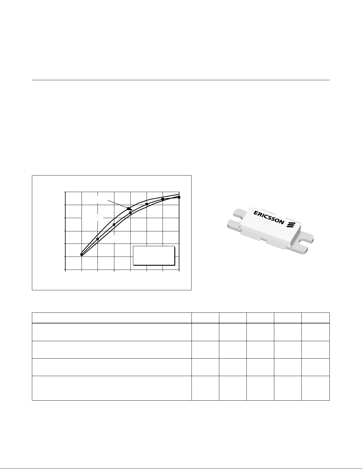
Typical Output Pow er vs. Input Pow er
150
125
100
75
50
25
Output Power (Watts
0
01234567
960 MHz
900 MHz
860 MHz
Input Power (Watts)
VDD = 28 V
= 1.4 A Total
I
DQ
INTERNALLY MATCHED
•
• Performance at 960 MHz, 28 Volts
- Output Power = 125 Watts
- Power Gain = 12.5 dB Typ
- Efficiency = 55% Typ
• Full Gold Metallization
• Silicon Nitride Passivated
• Back Side Common Source
• 100% Lot Traceability
10020
A-1234569813
Package 20240
RF Specifications (100% T ested)
Characteristic Symbol Min T yp Max Units
Gain
(V
Power Output at 1 dB Compression
(V
Drain Efficiency
(V
Load Mismatch Tolerance
(V
f = 959.9, 960 MHz—all phase angles at frequency of test)
All published data at T
= 28 V , P
DD
= 28 V , ICQ = 1.4 A T otal, f = 960 MHz) P-1dB 125 130 — Watts
DD
= 28 V , P
DD
= 28 V , P
DD
= 125 W, IDQ = 1.4 A Total, f = 960 MHz) G
OUT
= 125 W, IDQ = 1.4 A Total, f = 960 MHz) h 50 55 — %
OUT
= 125 W(PEP), IDQ = 1.4 A T otal, Y — — 10:1 —
OUT
= 25°C unless otherwise indicated.
CASE
ps
11.0 12.5 — dB
e
1
Page 2
PTF 10020
)
y
)
y
e
Electrical Characteristics (100% Tested—characteristics, conditions and limits shown per side)
Characteristic Conditions Symbol Min Typ Max Units
Drain-Source Breakdown Voltage VGS = 0 V , ID = 5 mA V
(BR)DSS
Drain-Source Leakage Current VDS = 28 V , VGS = 0 V I
Gate Threshold Voltage VDS = 10 V , ID = 75 mA V
Forward Transconductance VDS = 10 V , ID = 3 A g
DSS
GS(th)
fs
65 — — Volts
— — 1.0 mA
3.0 4.3 5.0 Volts
— 2 .5 — Siemens
Maximum Ratings
Parameter Symbol Value Unit
Drain-Source Voltage
Gate-Source Voltage
Operating Junction T emperature T
T otal Device Dissipation at P
Above 25°C derate by 1.67 W/°C
Storage T emperature Range T
Thermal Resistance (T
(1)
per side
(1)
(1)
= 70°C) R
CASE
V
V
DSS
GS
J
D
STG
qJC
65 Vdc
±20 Vdc
200 °C
290 Watts
–40 to +150 °C
0.6 °C/W
Typical Performance
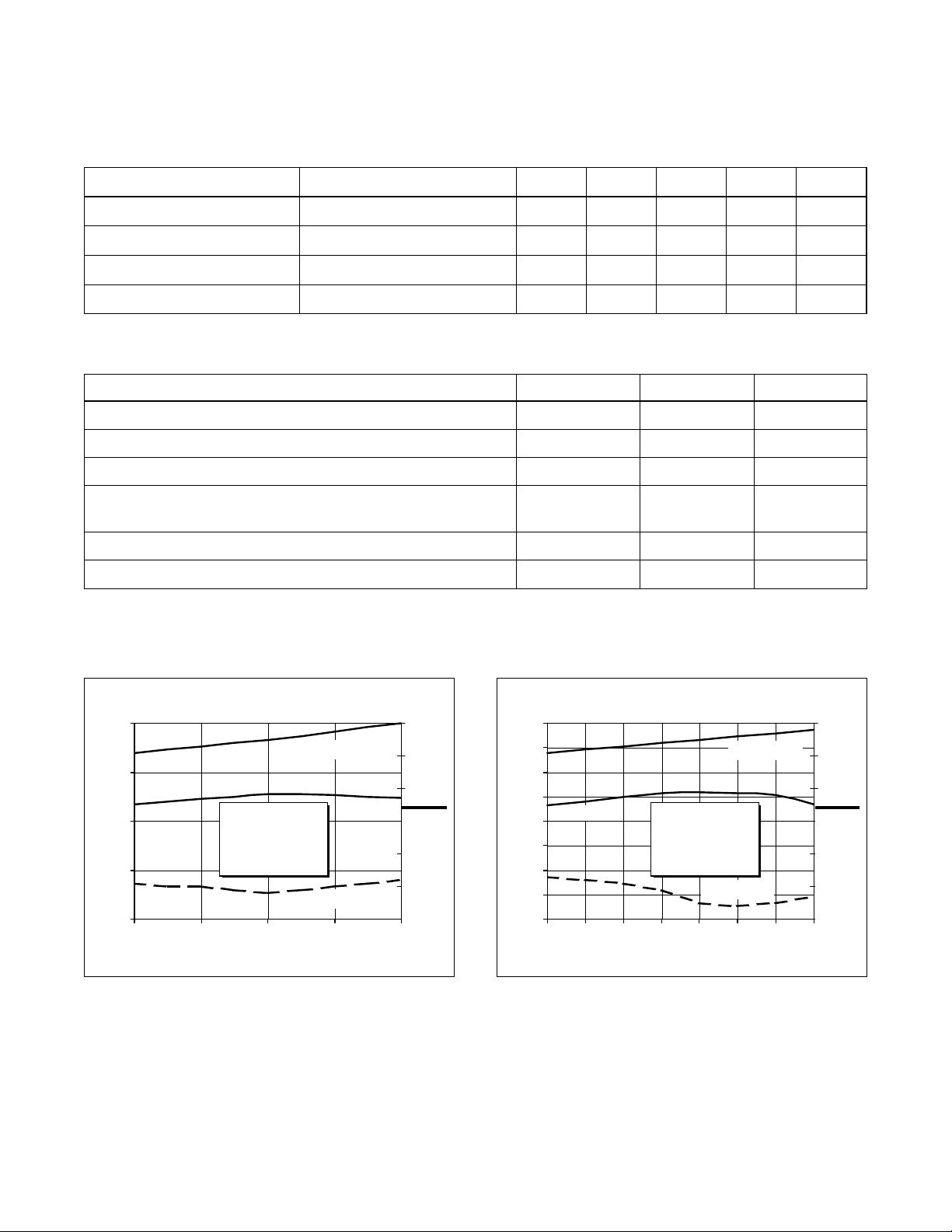
Broadband Test Fixtur e Performance
20
Efficiency %
16
Gain
12
Gain (dB)
8
4
860 870 880 890 900
VDD = 28 V
= 1.4 A Tota l
I
DQ
= 125 W
P
OUT
Return Loss
Frequency (MHz)
60
50
Efficienc
40
- 5
30
-15
20
-25
10
-35
0
Return Loss (dB
Broadband Test Fixtur e Performance
20
18
16
14
Gain
12
Gain (dB)
10
8
6
4
925 930 935 940 945 950 955 960
VDD = 28 V
= 1.4 A Tota l
I
DQ
P
OUT
Frequency (MHz)
Efficiency %
= 125 W
Return Loss
60
50
Efficienc
40
- 5
30
-15
20
-25
10
-35
0
Return Loss (dB
2
Page 3

e
)
I
I
Gain (dB )
Typical Performance
PTF 10020
Typical P
, Gain & Efficiency
OUT
(at P-1dB)
vs. Frequency
15
14
13
Gain
12
11
10
860 880 900 920 940 960
Frequ ency (MHz)
Output P ower (W)
VDD = 28 V
I
= 1.4 A Total
DQ
Efficienc y (% )
Output Power vs. Supply Voltage
150
130
110
90
70
Output Power (Watts)
50
20 22 24 26 28 30 32 34
VDS, Supply Voltage
IDQ = 1.4 A Tota l
f = 960 MHz
Pin = 5.4 W
150
130
110
90
70
50
Output Power & Efficiency
Efficiency vs. Output Power
80
70
60
50
40
30
Efficiency (%
20
10
0
30 50 70 90 110 130
VDD = 28 V
= 1.4 A Tota l
I
DQ
f = 960 MHz
Output Power (Watts)
Inter modulation Distortion vs. Output Power
-10
VDD = 28 V
-20
-30
-40
IMD (dBc)
-50
-60
= 1.4 A Tota l
I
DQ
= 941.9 MHz
f
1
= 942.0 MHz
f
2
20 30 40 50 60 70 80 90 100 110 120
3rd order
5th
7th
Output Power (Watts-PEP)
Power Gain vs. Output Power
15
= 1.4 A
DQ
14
= 700 m A
DQ
13
Gain (dB)
= 350 m A
I
DQ
12
11
1 10 100 1000
Output Power (W)
VDD = 28 V
f = 960 MHz
Capacitance vs. V oltage
180
160
140
C
120
100
80
60
Cds and Cgs (pF)
40
20
gs
C
ds
0
0 10203040
(one side)
VGS = 0 V
f = 1 MHz
C
rss
*
Supply Voltage (Volts)
*This part is internally matched. Measurements of the finished
product will not yield these figures.
3
27
24
21
18
15
12
9
6
3
0
Crss (pF)
Page 4

PTF 10020
Typical Performance
Impedance Data
Bias Voltage vs. Temper at ure
1.04
1.02
1.00
0.98
Bias Voltage (V)
0.96
0.94
-20 30 80 130
Voltage normalized to 1.0 V
Series show current (A)
Temp. (°C)
e
0.40
1.32
2.25
3.17
4.09
5.02
(VDD = 28 V , IDQ = 1.4 A, P
= 125 W)
OUT
Z Source Z Load
G
G
D
S
D
Frequency Z Source W Z Load W
MHz R jX R jX
835 1.7 -8.9 2. 3 -1.3
860 1.9 -9.3 2. 3 -0.9
885 1.9 -9.8 2. 3 -1.0
910 1.9 -11.8 2.2 -1.2
935 2.5 -12.9 2.2 -1.3
960 2.2 -12.8 2.2 -2.1
Z0 = 50 W
985 1.8 -11.0 2.2 -2.2
4
Page 5

e
PTF 10020
T ypical Scattering Parameters (one side only)
(VDS = 28 V, ID = 4 A)
f S11 S21 S12 S22
(MHz) Mag Ang Mag Ang Mag Ang Mag Ang
800 0.974 176 0.657 -10.6 0.002 50.9 0.97 -172
810 0.974 175.9 0.66 -11.5 0.002 49 0.971 -172.1
820 0.974 175.7 0.662 -12.7 0.002 52.9 0.971 -172.3
830 0.974 175.6 0.666 -13.6 0.002 53.4 0.972 -172.4
840 0.972 175.4 0.669 -14.8 0.002 52.6 0.972 -172.5
850 0.972 175.4 0.672 -16 0.002 54.9 0.972 -172.7
860 0.971 175.2 0.674 -16.9 0.002 56.1 0.972 -172.8
870 0.969 175 0.679 -18 0.002 52.5 0.972 -172.8
880 0.968 174.9 0.686 -19.1 0.002 53.4 0.973 -173
890 0.966 174.8 0.695 -20.2 0.002 56.2 0.975 -173.1
900 0.964 174.7 0.705 -21.4 0.002 58.1 0.977 -173.2
910 0.963 174.6 0.716 -23 0.002 55.5 0.977 -173.4
920 0.961 174.3 0.729 -24.6 0.002 57.7 0.976 -173.6
930 0.958 174.2 0.743 -26.3 0.002 57 0.977 -173.6
940 0.956 174.1 0.757 -28.2 0.002 56.7 0.978 -173.8
950 0.953 174 0.774 -30.3 0.002 58.7 0.979 -174
960 0.95 173.8 0.791 -32.7 0.002 60.2 0.979 -173.9
970 0.946 173.8 0.807 -35.4 0.002 60 0.981 -174.1
980 0.942 173.7 0.821 -38.1 0.002 59.5 0.982 -174.2
990 0.937 173.6 0.838 -41 0.002 62 0.983 -174.3
1000 0.933 173.6 0.853 -44 0.002 62.2 0.983 -174.4
Test Circuit
Schematic for f = 960 MHz
DUT PTF 10020
C1-2 15 pF, Capacitor A TC 100 B
C3 0.35–3.5 pF , V ariable Capacitor
C4 7.5 pF , Capacitor ATC 100 A
C5 1–9 pF , V ariable Capacitor
C6-7, C10, C13-14, C18 33 pF , Capacitor A TC 100 B
C8, C11 10 mF , +10 V Electrolytic Capacitor
C9, C12, C15, C19 0.01 mF , Capacitor A TC 100 B
C16, C17, C20, C21 10 mF , +30 V Electrolytic Capacitor
L1. L2 4 Turn, #20 A WG, .120” I.D.
R1, R2, R4, R5 1.0 K, W Resistor
R3, R6 5.1 K, 1/4 W Resistor
l1, l20 50 W, .030 l
l2, l19 20 W, .080 l
l3, l18 32 W, .191 l
l4, l17 25 W, .500 l
l5, l6 25 W, .091 l
l7, l10 7 W, .056 l
l8, l9 13.0 W, .017 l
l11, l12 13.0 W, .017 l
l13, l14 7.0 W, .093 l
l15, l16 10.2 W, .030 l
Circuit Board .028" Dielectric Thickness,
AlliedSignal, G200, 2 oz. copper
e
r
= 4.0,
5
Page 6

PTF 10020
Components Layout (not to scale)
e
Artwork (1 inch )
Ericsson Microelectronics
RF Power Products
Morgan Hill, CA 95037 USA
1-877-GOLDMOS (465-3667) United States
+46 8 757 4700 International
e-mail: rfpower@ericsson.com
www.ericsson.com/rfpower
6
Specifications subject to change without notice.
L3
© 1998 Ericsson Inc.
EUS/KR 1301-PTF 10020 Uen Rev. A 01-15-00
 Loading...