

Page 1
PTF 10019
r
70 Watts, 860–960 MHz
GOLDMOS
™
Field Effect T ransistor
Description
The PTF 10019 is an internally matched, 70 Watt LDMOS FET intended
for cellular, GSM, and D-AMPS applications in the 860 to 960 MHz
range. Nitride surface passivation and full gold metallization ensure
excellent device lifetime and reliability.
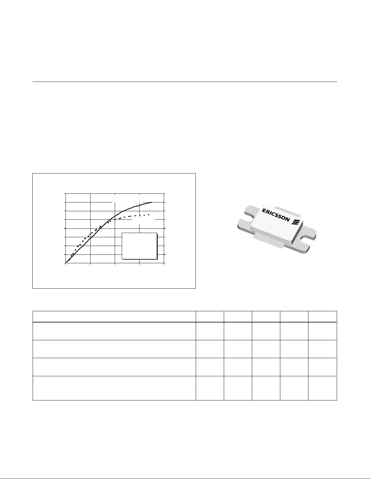
Typical Output Pow er vs. Input Pow er
80
60
40
20
Output Power (Watts)
0
0.0 1.0 2.0 3.0 4.0
Input Power (Wa tts)
Output P owe
Efficiency
VDD = 28 V
I
= 600 mA
DQ
f = 960 MHz
74
66
58
50
42
34
26
18
10
Efficiency (%)
INTERNALLY MA TCHED
•
• Performance at 960 MHz, 28 Volts
- Output Power = 70 Watts
- Power Gain = 14.5 dB Typ
- Efficiency = 50% Typ
• Full Gold Metallization
• Silicon Nitride Passivated
• Excellent Thermal Stability
• 100% Lot Traceability
10019
A-1234568955
Package 20237
RF Specifications (100% T ested)
Characteristic Symbol Min T yp Max Units
Gain
(V
Power Output at 1 dB Compression
(V
Drain Efficiency
(V
Load Mismatch Tolerance
(V
—all phase angles at frequency of test)
All published data at T
= 28 V , P
DD
= 28 V , IDQ = 600 mA, f = 960 MHz) P-1dB 70 75 — Watts
DD
= 28 V , P
DD
= 28 V , Pout = 70 W , IDQ = 600 mA, f = 960 MHz Y — — 10:1 —
DD
= 70 W, IDQ = 600 mA, f = 960 MHz) G
out
= 70 W, IDQ = 600 mA, f = 960 MHz) h 45 50 — %
out
= 25°C unless otherwise indicated.
CASE
pe
13.0 14.5 — dB
e
1
Page 2
PTF 10019
y
R
(dB)
y
s
e
Electrical Characteristics (100% T ested)
Characteristic Conditions Symbol Min Typ Ma x Units
Drain-Source Breakdown Voltage VGS = 0 V , ID = 25 mA V
(BR)DSS
Drain-Source Leakage Current VDS = 26 V , VGS = 0 V I
Gate Threshold Voltage VDS = 10 V , ID = 75 mA V
Forward Transconductance VDS = 10 V , ID = 3 A g
DSS
GS(th)
fs
65 — — Volts
— — 1.0 mA
3.0 — 5.0 Volts
— 3.0 — Siemens
Maximum Ratings
Parameter Symbol Value Unit
Drain-Source Voltage V
Gate-Source Voltage V
Operating Junction T emperature T
T otal Device Dissipation P
DSS
GS
J
D
Above 25°C derate by 1.25 W/°C
Storage T emperature Range T
Thermal Resistance (T
= 70°C) R
CASE
STG
qJC
65 Vdc
±20 Vdc
200 °C
215 Watts
–40 to +150 °C
0.8 °C/W
Typical Performance
Typical P
16
15
14
Power G ai n (d B )
13
, Gain, and Efficiency
OUT
vs. Frequency
Outp ut P ower (W)
Power Gain @ P-1dB
12
800 850 900 950 1000
Frequency (MHz)
(at P-1 dB)
Efficiency (%)
90
80
70
60
50
Output Power and Efficienc
16
14
12
10
Gain
8
6
4
900 915 930 945 960
Broadband Test Fixture Performance
Gain (dB)
Efficiency (%)
VDD = 28 V, IDQ = 600 mA, P
eturn Loss
Frequency (MHz)
OUT
= 70 W
70
60
50
40
- 5
30
-15
20
-25
10
Efficienc
Return Los
2
Page 3

e
I
I
I
r
)
PTF 10019
Power Gain vs. Output Power
18
17
16
15
14
13
Gain (dB)
12
11
10
= 600 mA
DQ
= 300 mA
DQ
= 150 mA
DQ
0.1 1.0 10.0 100.0
Output Power (Watts)
Inter modulation Distortion vs. Output Power
-10
VDD = 28 V
-20
-30
-40
IMD (dBc)
-50
-60
= 600 mA
I
DQ
= 959.900 MHz
f
1
= 960.000 MHz
f
2
0 1020304050607080
3rd Orde
5th
7th
Output Power (W atts-PEP)
Output Power
90
85
80
75
70
65
60
Output Power (Watts)
55
23 2 5 27 29 31 33
(at P-1dB)
vs. Supply Voltage
f = 960 MHz
= 600 mA
I
DQ
Drain-Source Voltage (Volts)
200
180
160
140
120
100
80
60
Cds and Cgs (pF
40
20
Capacitance vs. Voltage *
VGS = 0 V
f = 1 M Hz
C
gs
C
ds
C
rss
0
0 10203040
Supply Voltage (Volts)
20
18
16
14
12
10
8
6
4
2
0
Crss (pF)
* This part is internally matched. Measurements of the
finished product will not yield these figures.
Bias Voltage vs. Temper at ure
1.04
1.02
1.00
0.98
Bias Voltage (V)
0.96
0.94
-20 30 80 130
Voltage normalized to 1.0 V
Series show current (A)
0.40
1.32
2.25
3.17
4.09
5.02
Temp. (°C)
3
Page 4

PTF 10019
Impedance Data
e
(VDD = 28 V , Pout = 70 W , IDQ = 600 mA)
D
Z Source Z Load
G
S
Frequency Z Source W Z Load W
MHz R jX R jX
840 0.9 0 2.3 1.7
860 1.0 -0.2 2.0 1.6
900 1.2 -0.4 1.8 1.6
920 1.2 -0.4 1.7 1.6
960 1.8 -0.7 1.6 1.7
980 2.2 -0.6 1.6 1.8
Test Circuit
Z0 = 10 W
T est Circuit Schematic for f = 960 MHz
DUT PTF 10019 LDMOS Field Effect T ransistor
l1, l6 Microstrip 50 W
l2 0.125 l 960 GHz Microstrip 50 W
l3 0.186 l 960 GHz Microstrip 10 W
l4 0.200 l 960 GHz Microstrip 7.5 W
l5 0.060 l 960 GHz Microstrip 50 W
C1, C2, C4, C6 36 pF Chip Cap ATC 100 B
C3 3.6 pF Chip Cap ATC 100 A
C5 0.01 mF Capacitor Digi-Key P4917-ND
4
C7 50 mF , 35 V Electrolytic Capacitor,
Digi-Key P5276
C8 1.7 pF Chip Cap ATC 100 B
L1 4 T urn, #20 A WG, .120"I.D.
R1, R2, R3 220 W, 1/4 W Resistor
R4 10K W, 1/4 W Resistor
Circuit Board .028" Dielectric Thickness,
AlliedSignal, G200, 2 oz. copper
e
r
= 4.0,
Page 5

e
Components Layout (not to scale)
PTF 10019
10019
Artwork (1 inch )
Ericsson Microelectronics
RF Power Products
Morgan Hill, CA 95037 USA
1-877-GOLDMOS (465-3667) United States
+46 8 757 4700 International
e-mail: rfpower@ericsson.com
www.ericsson.com/rfpower
5
Specifications subject to change without notice.
L3
© 1997 Ericsson Inc.
EUS/KR 1301-PTF 10019 Uen Rev . A 10-22-99
Page 6

Notes:
eeeeeeeeeee
6
 Loading...