

Page 1
PT4181
White LED Step-Up Converter
GENERAL DESCRIPTION
The PT4181 is a step-up DC/DC converter designed for
driving up to 8 white LEDs in series from a single cell
Lithium Ion battery with constant current. Because it
directly regulates output current, the PT4181 is ideal for
driving light emitting diodes (LEDs) whose light
intensity is proportional to the current passing through
them, not the voltage across their terminals. A single
external resistor sets LED current between 5mA and
20mA, which can then be easily adjusted using either a
DC voltage or a pulse width modulated (PWM) signal.
Its low 104mV feedback voltage reduces power loss
and improves efficiency. The OV pin monitors the
output voltage and turns off the converter if an
over-voltage condition is present due to an open circuit
condition. The PT4181 is available in SOT23-6
packages.
ORDERING INFORMATION
PACKAGE
TEMPERATURE
RANGE
ORDERING PART
NUMBER
FEATURES
z Drives Up to 5 Series White LEDs from 2.5V
z Drives Up to 8 Series White LEDs from 3.6V
z Up to 87% Efficiency
z 1.2MHz Fixed Switching Frequency
z Low 104mV Feedback Voltage
z Open Load Shutdown
z Soft Start/PWM Dimming
z SOT23-6 Packages
APPLICATIONS
z Cell Phones
z Handheld Computers and PDAs
z Digital Cameras
z Small LCD Displays
TRANSPORT
MEDIA
MARKING
SOT23-6 -40 oC to 85 oC PT4181E23F
Tape and Reel
3000 units
4181
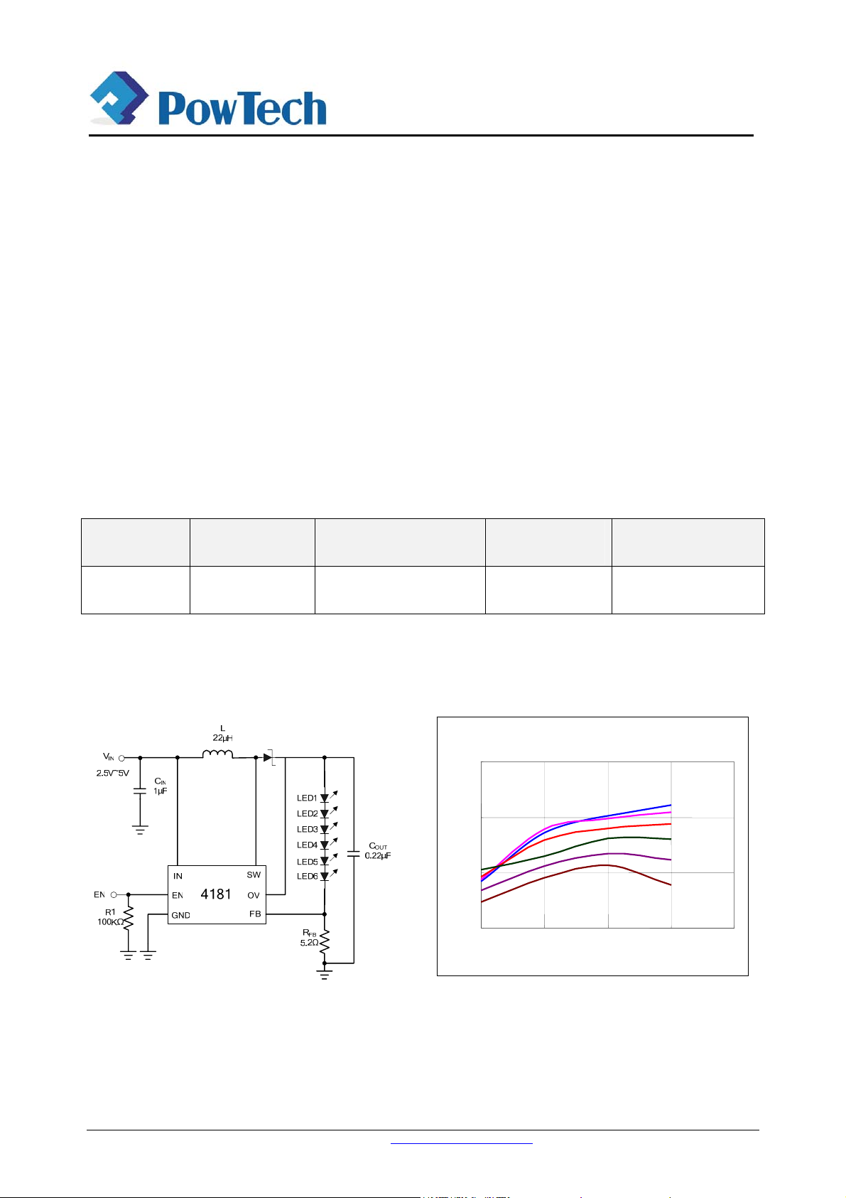
TYPICAL APPLICATIONS KEY PERFORMANCE CHART
Efficiency vs n(LED)
90.00%
85.00%
80.00%
75.00%
51015
20 25
Iout (mA) Vin=3.6V
3LED
4LED
5LED
6LED
7LED
8LED
Figure1. Li-Ion Driver for Six White LEDs Figure2. Efficiency vs Number of LEDs
China Resources Powtech (Shanghai) Limited WWW.CRPOWTECH.COM Page 1
PT4181_DS Rev EN_2.1
Page 2
PT4181
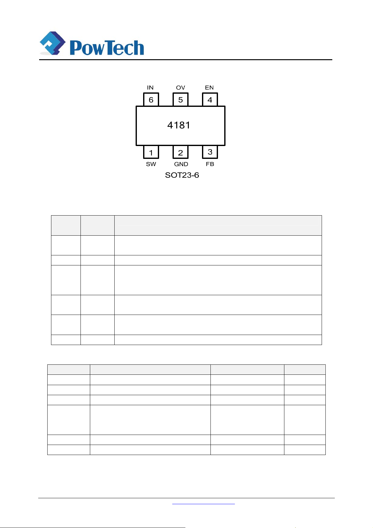
PIN ASSIGNMENT
PIN DESCRIPTIONS
SOT
PIN No.
1 SW Power Switch Output. Connect the inductor and the blocking Schottky diode to
2 GND Ground
3 FB Feedback input pin. The reference voltage at this pin is 104mV. Connect the
4 EN Enable pin. A high input at EN enables the device and a low input disables the
5 OV Over Voltage Input. OV measures the output voltage for open circuit protection.
6 IN Input Supply Pin. Must be locally bypassed.
PIN
Names
White LED Step-Up Converter
DESCRIPTION
SW.
cathode of the lowest LED to FB and a current sense resistor between FB and
GND.
devices. When not used, connect EN to the input source for automatic startup.
Connect OV to the output at the top of the LED string.
ABSOLUTE MAXIMUM RATINGS (Note 1)
SYMBOL ITEMS VALUE UNIT
VIN Input Voltage
VSW Voltage at SW Pin
VIO All Other I/O Pins GND-0.3 to VDD+0.3 V
Thermal Resistance,SOT-23-6
P
TR1
Tstg Storage Temperature -55 to 150
Tsolder Package Lead Soldering Temperature 260 , 10s℃
θ
θ
JA
JC
-0.3~6
-0.5~35
220
110
V
V
℃/W
℃
China Resources Powtech (Shanghai) Limited WWW.CRPOWTECH.COM Page 2
PT4181_DS Rev EN_2.1
Page 3
PT4181
White LED Step-Up Converter
RECOMMENDED OPERATING RANGE (Note 2)
SYMBOL ITEMS VALUE UNIT
VIN VIN Supply Voltage 2.5 to +6 V
VSW Output Voltage VIN to 28 V
T
Operating Temperature -40 to +85
OPT
℃
Note 1: Absolute Maximum Ratings indicate limits beyond which damage to the device may occur.
Note 2: Recommended operating Range indicates conditions for which the device is functional, but does not guarantee specific
performance limits.
ELECTRICAL CHARACTERISTICS (Note 3,4,5)
V
SYMBOL ITEMS CONDITIONS Min. Typ. Max. UNIT
Feedback
Operating Current
Chip Enable
Output Switch
Open Circuit Protection
Soft Start
=3V, Topt=25℃ unless specified otherwise.
IN=VEN
VIN Input Voltage 2.5 6 V
VFB FB Pin Voltage 89 104 119 mV
Ibias FB Pin Input Bias Current 0.05 1 µA
Ioff
Isby
Operating Current(Shutdown)
Operating Current(Quiescent)
V
=0V 0.1 1 µA
SW-ON
VFB=0.3V 100 350 µA
Fsw Switching Frequency 1.0 1.25 1.5 MHz
Dmax Maximum Duty Cycle VFB=0V 85 90 %
V
EN Minimum High Level 1.5 V
EN_H
V
EN Maximum Low Level 0.4 V
EN_L
V
EN Hysteresis 90 mV
HYS
EN Input Bias Current V
=0V, 5V 1 µA
SW-ON
RON SW On Resistance (Note 3) 0.5 Ω
I
SW Current Limit 400 mA
LIMIT
I
SW Leakage Current
LEAK
VOV Open Circuit Shutdown
Vsw=5V
VOV Rising 30 V
0.01 1 µA
Threshold
tss Soft Start Time (Note 3) V
Power On 160 µS
IN
Note 3: Electrical Characteristics state DC and AC electrical specifications under particular test conditions which
guarantee specific performance limits. This assumes that the device is within the recommended operating Range.
Specifications are not guaranteed for parameters where no limit is given, however, the typical value is a good
indication of device performance.
Note 4: Typicals are measured at 25˚C and represent the parametric norm.
Note 5:
China Resources Powtech (Shanghai) Limited WWW.CRPOWTECH.COM Page 3
PT4181_DS Rev EN_2.1
Datasheet min/max specification limits are guaranteed by design, test, or statistical analysis.
Page 4

PT4181
White LED Step-Up Converter
SIMPLIFIED BLOCK DIAGRAM
Figure 3. Simplified Block Diagram of the PT4181
OPERATION DESCRIPTION
The PT4181 uses a constant frequency, peak current
mode boost regulator architecture to regulate the series
string of white LEDs. The operation of the PT4181 can
be understood by referring to the simplified block
diagram shown above. At the start of each oscillator
cycle, the control logic turns on the power switch M1.
The signal at the non-inverting input of the PWM
comparator is proportional to the switch current,
summed together with a portion of the oscillator ramp.
When this signal reaches the level set by the output of
error amplifier, the PWM comparator resets the latch in
the control logic and turns off the power switch. In this
manner, error amplifier sets the correct peak current
level to keep the LED current in regulation. If the
feedback voltage starts to drop, the output of the error
amplifier increases. This results in more current to flow
through M1, hence increasing the power delivered to
the output.
TYPICAL PERFORMANCE CHARACTERISTICS
Driving Capability
100.00%
95.00%
90.00%
85.00%
80.00%
75.00%
70.00%
Efficiency vs Vin and I
Efficiency vs. Vin
3
3.13.23.3
3.43.53.63.7 3.83.9
Vin I
2.5V
3.0V
3.6V
LED
20mA
15mA
10mA
5mA
4
4.14.24.34.44.5
Vin (V)
=15mA I
LED
5 x LED 4 x LED
6 x LED 5 x LED
8 x LED 8 x LED
Efficiency
90.00%
89.00%
88.00%
87.00%
86.00%
85.00%
84.00%
83.00%
82.00%
81.00%
80.00%
-50 0 50 100 150
=20mA
LED
Efficiency vs Temperature
Efficiency vs. Temperature
20mA
15mA
10mA
Temp (C)
China Resources Powtech (Shanghai) Limited WWW.CRPOWTECH.COM Page 4
PT4181_DS Rev EN_2.1
Page 5

PT4181
White LED Step-Up Converter
TYPICAL PERFORMANCE CHARACTERISTICS
Quiescent Current vs VIN and Temperature
Iq VS Temperature
250
200
150
100
Iq(uA)
50
0
2.5 3 3.5 4 4.5 5 5.5 6
Vin(V)
Temp=-40℃
Temp=25℃
Temp=100℃
APPLICATION INFORMATION
Inductor Selections
For most of the applications of the PT4181, it is
recommended to use an inductor of 22uH. Although
small size is one of the major factors in selecting an
inductor, the smaller and thinner inductors give higher
core losses at 1.25MHz and DRC, resulting in lower
efficiencies. The following tab le provides a list of
recommended inductors:
Part
Number
LQH3C220 0.71 250 MURATA
CDRH3D16-220 0.53 350 SUMIDA
LB2012B220M 1.7 75 TAIYO YUDEN
LEM2520-220 5.5 125 TAIYO YUDEN
EJPC220KF 4.0 160 PANASONIC
DCR
(Ω)
Capacitor Selection
The small size of ceramic capacitors makes them ideal
for PT4181 applications. X5R and X7R types are
recommended because they retain their capacitance
over wider voltage and temperature ranges than other
types such as Y5V or Z5U. A 1μF input capacitor and a
0.22 μF output capacitor are sufficient for most PT4181
applications.
Diodes Selection
Schottky diodes, with their low forward voltage drop
and fast reverse recovery, are the ideal choices for
PT4181 applications. The forward voltage drop of a
Schottky diode represents the conduction losses in the
Current
Rating
(mA)
Manufacture
diode, while the diode capacitance (C
represents the switching losses. For diode selection,
both forward voltage drop and diode capacitance need
to be considered. Schottky diodes with higher current
ratings usually have lower forward voltage drop and
larger diode capacitance, which can cause significant
switching losses at the 1.25MHz switching frequency
of the PT4181. A Schottky diode rated at 100mA to
200mA is sufficient for most PT4181 applications.
Some recommended Schottky diodes are listed in the
following table:
CMDSH-3 100 0.58@100mA 7.0@10V Central
CMDSH2-3 200 0.49@200mA 15@10v Central
BAT54 200 0.53@100mA 10@25v Zetex
LED Current Control
The LED current is controlled by the feedback resistor.
The feedback reference is 104mV. The LED current is
104mV/Rfb. In order to have accurate LED current,
precision resistors are preferred (1% is recommended).
The formula and table for R
below:
Switching Frequency vs Temperature
1.6
1.4
1.2
1
0.8
0.6
Fosc(MHz)
0.4
0.2
0
Part
Number
I
LED
Fosc VS Temp.
-40 25 100
Temp(℃)
or CD)
T
Forward
Current
(mA)
RFB = 104mV/I
Voltage
Drop
(V)
selection are shown
FB
LED
Diode
CAP
(Pf)
Manu
facture
(mA) RFB Valu e (Ω)
5 20.8
10 10.4
15 6.93
20 5.2
China Resources Powtech (Shanghai) Limited WWW.CRPOWTECH.COM Page 5
PT4181_DS Rev EN_2.1
Page 6

PT4181
White LED Step-Up Converter
Open Circuit Protection
Open circuit protection will shut off the PT4181 if the
output voltage goes too high when the OV pin is tied to
the output. In some cases an LED may fail, which will
result in the feedback voltage always being zero. The
PT4181 will then switch at its maximum duty cycle
boosting the output voltage higher and higher. By
connecting the OV pin to the top of the LED string the
PT4181 checks this condition and if the output ever
exceeds 30V, the PT4181will shut down. The part will
not switch again until the power is recycled.
Dimming Control
There are three different types of dimming control
circuits:
1. Using a DC Voltage
For some applications, the preferred method of
brightness control is a variable DC voltage to adjust the
LED current. The dimming control using a DC voltage
is shown in Figure 3. As the DC voltage increases, the
voltage drop on R2 increases and the voltage drop on
R1 decreases. Thus, the LED current decreases. The
selection of R2 and R3 will make the current from the
variable DC source much smaller than the LED current
and much larger than the FB pin bias current.
Figure4. Dimming Control Using a PWM Signal
3. Using a Filtered PWM Signal
The filtered PWM signal can be considered as an
adjustable DC voltage. It can be used to replace the
variable DC voltage source in dimming control. The
circuit is shown in Figure 5.
Figure3. Dimming Control Using a DC Voltage
2. Using a PWM Signal to EN Pin
With the PWM signal applied to the EN pin, the PT410
is turned on or off by the PWM signal. The LEDs
operate at either zero or full current. The average LED
current increases proportionally with the duty cycle of
the PWM signal. A 0% duty cycle will turn off the
PT4181 and corresponds to zero LED current. A 100%
duty cycle corresponds to full current. The typical
frequency range of the PWM signal should be 1kHz or
less due to the soft start function.
Figure5. Dimming Control Using a Filtered PWM Signal
Start-up and Inrush Current
The PT4181has internal soft start to limit the amount of
current through VIN at startup and to also limit the
amount of overshoot on the output. The soft start is
realized by gradually increasing the current limit during
start-up. The current limit is increased by a third every
60μS giving a total soft start time of around 180μS.
Board Layout Consideration
As with all switching regulators, careful attention must
be paid to the PCB board layout and component
placement. To maximize efficiency, switch rise and fall
times are made as short as possible. To prevent
electromagnetic interference (EMI) problems, proper
layout of the high frequency switching path is essential.
The voltage signal of the SW pin has sharp rise and fall
edges. Minimize the length and area of all traces
connected to the SW pin and always use a ground plane
under the switching regulator to minimize interplane
coupling. In addition, the ground connection for the
feedback resistor R1 should be tied directly to the GND
pin and not shared with any other component, ensuring
a clean, noise-free connection.
China Resources Powtech (Shanghai) Limited WWW.CRPOWTECH.COM Page 6
PT4181_DS Rev EN_2.1
Page 7

PT4181
PACKAGE INFORMATION
E1
White LED Step-Up Converter
SOT23-6
D
b
E
e
e1
θ
0.2
L1
L
c
A1
A
A2
SYMBOL
A 1.050 1.250 0.041 0.049
A1 0.000 0.100 0.000 0.004
A2 1.050 1.150 0.041 0.045
b 0.300 0.400 0.012 0.016
c 0.100 0.200 0.004 0.008
D 2.820 3.020 0.111 0.119
E 1.500 1.700 0.059 0.067
E1 2.650 2.950 0.104 0.116
e 0.950TYP 0.037TYP
e1 1.800 2.000 0.071 0.079
L 0.700REF 0.028REF
L1 0.300 0.600 0.012 0.024
θ 0° 8° 0° 8°
MILLIMETERS INCHES
MIN MAX MIN MAX
China Resources Powtech (Shanghai) Limited WWW.CRPOWTECH.COM Page 7
PT4181_DS Rev EN_2.1
Page 8

 Loading...