

MITSUMI
System Reset (with battery back-up) PST620, 621
System Reset (with battery back-up)
Monolithic IC PST620, 621
Outline
Features
1. Low current consumption
2. Capacitors (super capacitor, large capacity chemical capacitor) are used for back-up power supply, lowering
system cost
3. Stable 1-chip microcomputer crystal oscillator rise time maintained with the built-in pulse shaver.
4. In addition to power outage detection for main power supply (+5V), there are built-in pins to detect AC power
supply and +5V power supply primary side
5. Reset signal output by back-up power supply (super capacitor, large capacity chemical capacitor) detection
Applications
1. VCR
2. Audio equipment
3. Communications equipment
4. Rice cookers, etc.
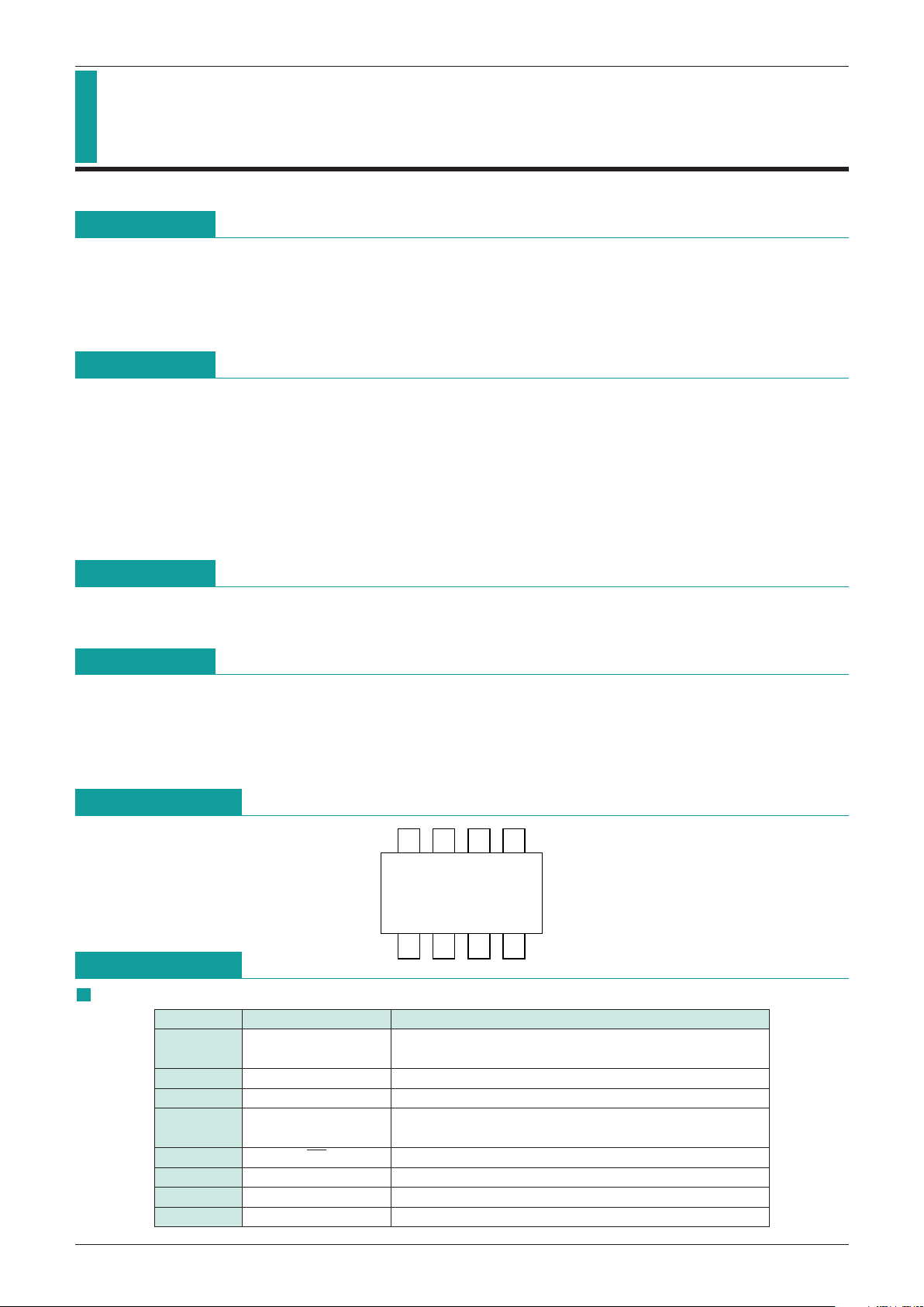
Pin Assignment
Pin Description
1432
8567
PST620
Pin No. Pin name Function
1 V
AC
Has +2.0V detection voltage to detect AC power supply and
stable power supply primary side, for quick power outage detection.
2 VCC1 +5V main power supply
3 V
CC2
Back-up power supply (back-up capacitor connected)
4 TC
Pulse width setting pin for pulse shaver
(capacitor and resistor connected)
5
RE
Reset output
6 PS
CONT
Pulse shaver ON/OFF switching High : OFF Low : ON
7 CE Chip enable signal output
8 GND GND
Package
DIP-8B (PST620DDB, PST621DDB)
SOP-8C (PST620DFT, PST621DFT)
These ICs are part of the regular series of back-up ICs, and use capacitors (super capacitor, large capacity
chemical capacitor) as back-up power supply. They control 1-chip microcomputer high-speed, low-speed,
and stand-by modes (MNI control).
These ICs also are capable of controlling data save in EPROM and other nonvolatile memories during power outage.
MITSUMI
System Reset (with battery back-up) PST620, 621
PST621
Pin No. Pin name Function
1 V
AC
Has +2.0V detection voltage to detect AC power supply and
stable power supply primary side, for quick power outage detection.
2 VCC1 +5V main power supply
3 V
CC2 Back-up power supply (back-up capacitor connected)
4 T
C
Pulse width setting pin for pulse shaver
(capacitor and resistor connected)
5 RE
---------------------------------------------------------------
Reset output
6 MODE
Switches 1-chip microcomputer mode with pulse
shaver output signal
7 CE
Chip enable signal output (power outage detection signal)
8 GND GND
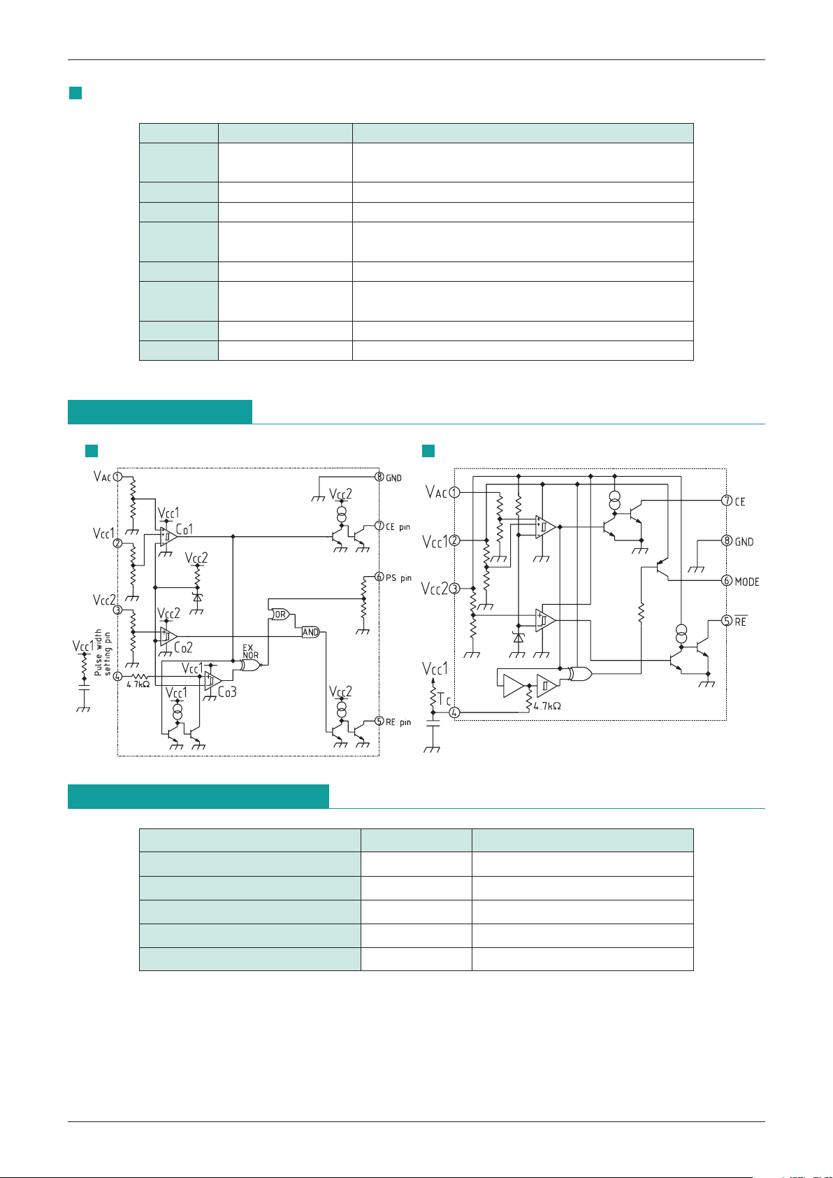
Block Diagram
PST620
PST621
Absolute Maximum Ratings
(Ta=25°C)
Item Symbol Rating
Storage temperature T
STG
-
40~+125°C
Operating temperature T
OPR
-
20~+70°C
Power supply voltage V
CC max.
-
0.3~+10V
TC input input voltage V
C max. VCC1+0.3V
Allowable loss Pd 450mW

MITSUMI
System Reset (with battery back-up) PST620, 621
Electrical Characteristics
(Ta=25°C)
Note 1 : *1 Connect TC pin to GND.
Note 2 : Except where noted otherwise, VAC=5V, Vc=OPEN.
Item Symbol Measurement conditions Min. Typ. Max. Units
Detection voltage 1 V
S1RL1=47kΩ CE output, VCC1=L H
*
1 4.00 4.20 4.40
Detection PST620
V
S2
R
L2=47kΩ, RE output 2.00 2.15 2.30
V
voltage 2 PST621 V
CC2=H L
*
1 2.90 3.10 3.30
Detection voltage 3 V
S3RL1=47kΩ, CE output, VAC=H L
*
1 1.85 2.00 2.15
Hysteresis voltage 1 V
S1RL1=47kΩ, CE output, VCC1=L H L 75 150 300
Hysteresis voltage 2 V
S2RL2=47kΩ, CE output, VCC2=L H L 25 50 100 mV
Hysteresis voltage 3 V
S3RL1=47kΩCE output, VAC=L H L 45 90 180
Detection voltage
V
S/ T RL1=47kΩ, CE output ±0.01
temperature coefficient 1
Detection voltage
V
S/ T RL2=47kΩ, RE output ±0.02 %/
°
C
temperature coefficient 2
Detection voltage
V
S/ T RL1=47kΩ, CE output ±0.01
temperature coefficient 3
Low-level output voltage 1 V
OL1
VCC1=VS1 min.-0.05V, R
L
1=47kΩ CE output
0.1 0.2
Low-level output voltage 2 V
OL2
VCC2=VS2 min.-0.05V, R
L
2=47kzΩ RE output
0.1 0.4
V
Low-level output voltage 3 V
OL3
V
CC1=0V, VCC2=VS2 typ./0.85
R
L1=47kΩ, CE output
0.2 0.4
Operation limit voltage 1 V
OP1RL1=47kΩ, VOL1
<
=
0.4V CE output 0.8 1.0
V
Operation limit voltage 2 V
OP2RL2=47kΩ, VOL2
<
=
0.4V RE output 0.8 1.0
Consumption current 1
I
CC1VCC1=VCC2=VS1/0.85 5.0 8.5
I
CC2RL1=RL2=∞ 2.0 3.5
Consumption current 2
I
CC1VCC1=VCC2=VS1 min.
-
0.05V 8.0 14.5
µA
I
CC2RL1=RL2=∞ 2.0 3.5
Consumption current 3
I
CC1VCC1=VCC2=VS2 min.
-
0.05V 8.0 14.5
I
CC2RL1=RL2=∞ 4.0 7.0
Consumption current 4 I
CC2
V
CC1=0V RL1=RL2=∞,
V
CC2=VS1T typ./0.85
2.0 3.5
µA
Consumption current 5 I
CC2
V
CC1=0V RL1=RL2=∞
V
CC2=VS2 min.
-
0.05V
4.0 7.0
Output current while on 1 I
OL1VCC1=VS1 min.
-
0.05V, RL1=0 CE output 2
mA
Output current while on 2 I
OL2VCC2=VS2 min.
-
0.05V, RL2=0 RE output 2
Transport delay time 1 T
PLH1
VCC1=VS1 typ.±0.4V, R
L
2=47kΩ CE output
10
Transport delay time 2 T
PLH2
VCC2=VS2 typ.±0.4V, R
L
2=47kΩ RE output
50
µS
Transport delay time 3 T
PLH3
VCC1=VS1 typ.±0.4V, R
L
2=47kΩ CE output
40
Transport delay time 4 T
PLH4
VCC2=VS2 typ.±0.4V, R
L
2=47kΩ RE output
80
AC pin input resistance R
ACIN 0.5 1.0 MΩ
One-shot pulse width T
pd
Cd=0.47µF Rd=100k, VCC1=VS1 typ.±0.4V
61421mS
One-shot output voltage V
TOL
VCC1=VS1typ./0.85, R
L
1=47kΩ RE output,
*
1
0.1 0.4 V
TC pin threshold voltage V
CTH RL1=47kΩ, VC=L H 2.0 V
TC input input current I
CIN VCC1=VS1 typ./0.85, VC=5.0V 1 µA
PS pin input H level voltage V
PSH 2.0 V
PS pin input L level voltage V
PSL 0.6 V
PS pin input H level current I
PSH VPSH=2.0V 10 µA

MITSUMI
System Reset (with battery back-up) PST620, 621
Characteristics
(PST620, 621 series. However, VS2 in PST620 series only.)
ICC1
(µA)
15.00
I
CC1
(µA)
15.00
.0000 .0000
.0000 10.00
1.500/div 1.500/div
1.000/div
V
CC1(V)
Current consumption
(V)
4.400
(V)
4.400
.0000 .0000
.0000 10.00
.4400/div .4400/div
.0900/div
V
CC1 (V)
VS1
(V)
2.300
.0000
2.100
.2300/div
(V)
2.300
.0000
2.300
.2300/div
V
CC1 (V)
.0200/div
VS2
CS
(V)
10.00
REST
(V)
10.00
.0000 .0000
.0000 10.00
1.000/div
1.000/div
1.000/div
V
CC1 (V)
VOL
10
5
0
-
250 255075
Pulse width (mS)
Temperature (°C)
1 shot pulse width-Temperature
4.30
4.20
4.10
-
25 0 25 50 75
Vs1 detection
voltage (V)
Temperature (°C)
Vs1 detection voltage-Temperature
2.20
2.10
2.00
-
25 0 25 50 75
Vs2 detection
voltage (V)
Temperature (°C)
Vs2 detection voltage-Temperature
2.10
2.00
1.90
-
250 255075
Vs3 detection
voltage (V)
Temperature (°C)
Vs3 detection voltage-Temperature

MITSUMI
System Reset (with battery back-up) PST620, 621
Timing Chart
VCC1
V
CC2
CE
TC
RE
CE
4.2V
2.15V
V
TX
Delay
Delay
Note : Connect V
AC pin to VCC when not using.
AC power supply
AC rectifier or
regulator
primary side
Note 1: VTH is set at 2.0V and hysteresis voltage at 90mV.
1. Use a resistor to divide the detected voltage so that it equals V
TH when monitoring regulator
primary side power supply.
2. When monitoring AC voltage rectified as in the application circuit, set so that it equals V
TH by
lowering the constant and dividing with a resistor. Refer to application circuit diagram.
Note 2: VAC input and VS1 are OR, so either signal makes CE low when power outage is detected.
PST620
PST621
AC
VCC1
CE
MODE
VCC2
RESET
4.2V
3.1V
Application Circuits
VAC input : Power supply transformer secondary voltage detection

MITSUMI
System Reset (with battery back-up) PST620, 621
1. Connection
1. +5V power supply to V
CC1 (Pin 2).
2. Connect back-up capacitor to V
CC2 (Pin 3).
3. Connect a diode between V
CC1 (Pin 2) and VCC2 (Pin 3).
4. Connect pulse width setting resistor and capacitor to PC (Pin 4) when using pulse shaver.
5. RE output (Pin 5) is reset signal output and is output when V
CC is less than 2.15V.
6. When using pulse shaver, P
SCONT (Pin 6) is high level.
7. CE output (Pin 7) is for chip enable signal and goes low when power outage is detected.
2. Theory of Operation
1. When +5V power is supplied normally, it is charged to the back-up capacitor via a diode.
2. The back-up capacitor starts back-up if +5V power supply voltage drops for some reason and
V
CC1 goes below 4.2V, and at the same time the CE
---------------------------------------------------
signal switches the 1-chip microcomputer to
standby mode, so that it operates on low current consumption.
3. When +5V power supply recovers and goes over 4.2V, an RE output signal of a certain width is
output, and this signal resets the 1-chip microcomputer. At the same time normal mode starts and
the time until crystal oscillator output stabilizes is reset.
4. If +5V power supply does not recover, and back-up capacitor voltage goes below 2.15V, reset is
carried out by the RE output signal to prevent the microcomputer from running wild.
3. Setting AC power supply power outage detection
1. Theory of operation for detecting AC voltage
AC voltage is rectified and smoothed by the capacitor. This voltage is divided and set at VAC input
detection voltage, +2V. At this time the smoothing capacitor and dividing resistor time constants
are used to set AC voltage missing waveform.
2. VAC voltage setting (R1, R2)
Set resistor ratio at the midpoint between R1 and R2 so that the voltage to be detected is +2V.
Impressed AC voltage
There is are no limitations on AC voltage as it is divided by R1 and R2 and applied to PST620.
3. Setting time constants to detect AC voltage (C4, R1+R2)
For impressed AC voltage of 5Vrms, and C4 and R1+R2 time constant of 60mS, set so that AC
voltage detects power outage when approximately 2 waveforms are missed. The time constants
can be set to detect missing AC waveforms.
Application Circuits
VAC input : Stable power supply primary voltage detection
 Loading...