

Page 1

ICs for Communications
ISDN Echocancellation Circuit for Terminal Applications
IEC-Q TE
PSB 21911 Version 5.2
PSF 21911 Version 5.2
Data Sheet 11.97
DS 1
Page 2

PSB 21911
Revision History: Original Version: 11.97
Previous Releases: None
Page Subjects (changes since last revision)
For questions on technology, delivery and prices please con tact the Semiconductor
Group Offices in Germany or the Siemens Companies and Representatives worldwide:
see our webpage at http://www.siemens.de/Semiconductor/address/address.htm.
Edition 11.97
Published by Siemens AG,
HL TS,
Balanstraße 73,
81541 München
©
Siemens AG 28.11.97.
All Rights Reserved.
Attention please!
As far as patents or other rights of third parties are concerned, liability is only assumed for components, not for
applications, processes and circui ts implemented within component s or assemblies.
The information describes the type of component and s hall not be considered as assured ch aracteristics.
Terms of delivery and rights to change design reserved.
Due to tec hnical requirements components may contain dangerous substances. For information on the types in
question please contact your nearest Siemens Off ice, Semiconductor Group.
Siemens AG is an approved CECC manufacturer.
Packing
Please use the recycling operators known to you. We can also help you – get in touch with your nearest sales
office. By agreement we will take packing material back, if it is sorted. You must bear the costs of transport.
For pac king mat erial that is ret urned to us unsorte d or wh ich we a re not oblig ed to a ccept, we shal l have to in v oice
you for any costs incurred.
Components used in life-support devices or systems must be expressly authorized for such purpose!
Criti cal compon ents1 of the Semiconductor Group of Siemens AG, may only be used in life-support devices or
systems2 with the express written approval of the Semiconductor Group of Siemens AG.
1 A critical component is a component used in a life-support devi ce or system whose failure can reasonably be
expected t o ca use t he f ail u re o f th at l ife- s upp ort devi ce o r s ys tem, or to af fe ct i t s saf et y or ef fe ct ive ness of t hat
device or system.
2 Life support devices or systems are intended (a) to be implanted in the human body, or (b) to support and/or
maintain and sustain human life. If they fail, it is reasonable to assume that the health of the user may be endangered.
Page 3

PSB 21911
PSF 21911
Table of Contents Page
1 Overview
1.1 Features . . . . . . . . . . . . . . . . . . . . . . . . . . . . . . . . . . . . . . . . . . . . . . . . . . .9
1.2 Logic Symbol µP Mode . . . . . . . . . . . . . . . . . . . . . . . . . . . . . . . . . . . . . . .10
1.3 Logic Symbol Stand-Alone Mode . . . . . . . . . . . . . . . . . . . . . . . . . . . . . . .11
1.4 Pin Configuration . . . . . . . . . . . . . . . . . . . . . . . . . . . . . . . . . . . . . . . . . . . .12
1.5 Pin Definitions and Functions . . . . . . . . . . . . . . . . . . . . . . . . . . . . . . . . . .13
1.6 Microprocessor Bus Interface (Overview) . . . . . . . . . . . . . . . . . . . . . . . . .21
1.7 System Integration . . . . . . . . . . . . . . . . . . . . . . . . . . . . . . . . . . . . . . . . . . .22
1.7.1 ISDN PC Adapter Card . . . . . . . . . . . . . . . . . . . . . . . . . . . . . . . . . . . . . . .22
1.7.2 ISDN Stand -Alone Termi nal with POTS Interface . . . . . . . . . . . . . . . . . . .23
1.7.3 ISDN Feat ure Phone . . . . . . . . . . . . . . . . . . . . . . . . . . . . . . . . . . . . . . . . .24
1.7.4 ISDN-Modem PC Card . . . . . . . . . . . . . . . . . . . . . . . . . . . . . . . . . . . . . . .25
2 Functional Description
2.1 Operating Modes . . . . . . . . . . . . . . . . . . . . . . . . . . . . . . . . . . . . . . . . . . . .26
2.2 Device Architecture . . . . . . . . . . . . . . . . . . . . . . . . . . . . . . . . . . . . . . . . . .28
2.3 IOM-2 Interface . . . . . . . . . . . . . . . . . . . . . . . . . . . . . . . . . . . . . . . . . . . . .30
2.3.1 IOM-2 Frame Structure . . . . . . . . . . . . . . . . . . . . . . . . . . . . . . . . . . . . . . .30
2.3.2 IOM-2 Command / Indication Channels . . . . . . . . . . . . . . . . . . . . . . . . . .34
2.3.3 IOM-2 Monitor Channel . . . . . . . . . . . . . . . . . . . . . . . . . . . . . . . . . . . . . . .35
2.3.4 Activation/Deactiva tion of IOM-2 Clocks . . . . . . . . . . . . . . . . . . . . . . . . . .37
2.3.5 Superframe Marker . . . . . . . . . . . . . . . . . . . . . . . . . . . . . . . . . . . . . . . . . .38
2.3.6 IOM-2 Output Driver Selection . . . . . . . . . . . . . . . . . . . . . . . . . . . . . . . . .38
2.4 Microprocessor Interface . . . . . . . . . . . . . . . . . . . . . . . . . . . . . . . . . . . . . .39
2.4.1 Microprocessor Clock Output . . . . . . . . . . . . . . . . . . . . . . . . . . . . . . . . . .39
2.4.2 Watchdog Timer . . . . . . . . . . . . . . . . . . . . . . . . . . . . . . . . . . . . . . . . . . . .39
2.5 U-Transceiver . . . . . . . . . . . . . . . . . . . . . . . . . . . . . . . . . . . . . . . . . . . . . .40
2.5.1 U-Frame Structure . . . . . . . . . . . . . . . . . . . . . . . . . . . . . . . . . . . . . . . . . . .42
2.5.2 EOC-Processor and MON-0 . . . . . . . . . . . . . . . . . . . . . . . . . . . . . . . . . . .51
2.5.3 Maintenance (MON-1) . . . . . . . . . . . . . . . . . . . . . . . . . . . . . . . . . . . . . . . .54
2.5.4 O verh ead Bits (MON-2) . . . . . . . . . . . . . . . . . . . . . . . . . . . . . . . . . . . . . . .56
2.5.5 Local Functions (MON-8) . . . . . . . . . . . . . . . . . . . . . . . . . . . . . . . . . . . . .59
2.5.6 State Machine Notation Rules . . . . . . . . . . . . . . . . . . . . . . . . . . . . . . . . . .62
2.5.7 State Machine . . . . . . . . . . . . . . . . . . . . . . . . . . . . . . . . . . . . . . . . . . . . . .63
2.5.8 C/I Codes . . . . . . . . . . . . . . . . . . . . . . . . . . . . . . . . . . . . . . . . . . . . . . . . . .74
2.5.9 Layer 1 Loop-Backs . . . . . . . . . . . . . . . . . . . . . . . . . . . . . . . . . . . . . . . . . .76
2.5.10 Analog Line Port . . . . . . . . . . . . . . . . . . . . . . . . . . . . . . . . . . . . . . . . . . . .78
2.6 Access to IOM-2 Channel s . . . . . . . . . . . . . . . . . . . . . . . . . . . . . . . . . . . .81
2.6.1 B-Channel Access . . . . . . . . . . . . . . . . . . . . . . . . . . . . . . . . . . . . . . . . . . .82
2.6.2 D-Channel Access . . . . . . . . . . . . . . . . . . . . . . . . . . . . . . . . . . . . . . . . . . .82
2.6.3 C/I Channel Access . . . . . . . . . . . . . . . . . . . . . . . . . . . . . . . . . . . . . . . . . .83
2.6.4 Monitor Channel Access . . . . . . . . . . . . . . . . . . . . . . . . . . . . . . . . . . . . . .84
2.7 S/G Bit and BAC Bit in TE Mode . . . . . . . . . . . . . . . . . . . . . . . . . . . . . . .89
. . . . . . . . . . . . . . . . . . . . . . . . . . . . . . . . . . . . . . . . . . . . . . . . . . .8
. . . . . . . . . . . . . . . . . . . . . . . . . . . . . . . . . . . . . .26
Semiconductor Group 3 11.97
Page 4

PSB 21911
PSF 21911
2.7.1 Applications with ELIC on the Linecard (PBX) . . . . . . . . . . . . . . . . . . . . .90
2.8 Reset . . . . . . . . . . . . . . . . . . . . . . . . . . . . . . . . . . . . . . . . . . . . . . . . . . . . .93
2.9 Power Controller Interface . . . . . . . . . . . . . . . . . . . . . . . . . . . . . . . . . . . . .94
3 Operational Description
. . . . . . . . . . . . . . . . . . . . . . . . . . . . . . . . . . . . .97
3.1 C/I Channel Programming . . . . . . . . . . . . . . . . . . . . . . . . . . . . . . . . . . . . .97
3.2 Monitor Channel Programming . . . . . . . . . . . . . . . . . . . . . . . . . . . . . . . . .98
3.3 Layer 1 Activation/Deactivation . . . . . . . . . . . . . . . . . . . . . . . . . . . . . . . .100
3.4 External Circuitry . . . . . . . . . . . . . . . . . . . . . . . . . . . . . . . . . . . . . . . . . . .109
3.4.1 Power Supply Blocking Recommendation . . . . . . . . . . . . . . . . . . . . . . . .109
3.4.2 U-Interface . . . . . . . . . . . . . . . . . . . . . . . . . . . . . . . . . . . . . . . . . . . . . . . .110
3.4.3 Oscillator Circuit . . . . . . . . . . . . . . . . . . . . . . . . . . . . . . . . . . . . . . . . . . .111
4 Register Description
. . . . . . . . . . . . . . . . . . . . . . . . . . . . . . . . . . . . . . .112
4.1 Interrupt Structure . . . . . . . . . . . . . . . . . . . . . . . . . . . . . . . . . . . . . . . . . .114
4.1.1 Monitor-Channel Interrupt Logic . . . . . . . . . . . . . . . . . . . . . . . . . . . . . . .115
4.2 Registers . . . . . . . . . . . . . . . . . . . . . . . . . . . . . . . . . . . . . . . . . . . . . . . . .116
5 Electrical Characteristics
. . . . . . . . . . . . . . . . . . . . . . . . . . . . . . . . . . .130
5.1 Absolute Maximum Ratings . . . . . . . . . . . . . . . . . . . . . . . . . . . . . . . . . . .130
5.2 Power Consumption . . . . . . . . . . . . . . . . . . . . . . . . . . . . . . . . . . . . . . . .132
5.3 DC Characteristics . . . . . . . . . . . . . . . . . . . . . . . . . . . . . . . . . . . . . . . . . .133
5.4 AC Characteristics . . . . . . . . . . . . . . . . . . . . . . . . . . . . . . . . . . . . . . . . . .136
5.4.1 Parallel Microprocessor Interface Timing . . . . . . . . . . . . . . . . . . . . . . . .136
5.4.2 Serial Microprocessor Interface Timing . . . . . . . . . . . . . . . . . . . . . . . . . .140
5.4.3 IOM-2 Interface Timing . . . . . . . . . . . . . . . . . . . . . . . . . . . . . . . . . . . . . .142
6 Package Outlines
7 External Component Sourcing
8 Glossary
. . . . . . . . . . . . . . . . . . . . . . . . . . . . . . . . . . . . . . . . . . . . . . . . .152
. . . . . . . . . . . . . . . . . . . . . . . . . . . . . . . . . . . . . . . . . .147
. . . . . . . . . . . . . . . . . . . . . . . . . . . . . . .149
Appendix
App A Jitter on IOM-2 . . . . . . . . . . . . . . . . . . . . . . . . . . . . . . . . . . . . . . . . . . . . .154
App B S/G Bit Control State Machine . . . . . . . . . . . . . . . . . . . . . . . . . . . . . . . . .155
App C Quick Reference Guide . . . . . . . . . . . . . . . . . . . . . . . . . . . . . . . . . . . . . .160
Index
IOM®, IOM®-1, IOM®-2, SIC OF I®, SICOFI®-2, SICOFI®-4, SIC OF I®-4µC, SLICOFI®, ARCOFI
ARCOFI®-SP, EPIC®-1, EPIC®-S, ELIC®, IPAT®-2, ITAC®, ISAC®-S, ISAC®-S TE, ISAC®-P, ISAC®-P TE, IDEC®,
SICAT®, OCTAT®-P, QUA T®-S are registered trademarks of Siemens AG.
MUSAC™-A, FALC™54, IWE™, SARE™, UTPT™, ASM™, ASP™, DigiTape™ are trademarks of Siemens AG.
2
Purchase of Sie mens
2
I
the
C-syst em provided t he system conf orms to the
I
C components conveys a license under the Philips’
2
I
C specifications defined by Philips. Copyright Philips 1983.
2
I
C patent to use the components in
®
, ARCOFI®-BA,
Semiconductor Group 4 11.97
Page 5

PSB 21911
PSF 21911
List of Figures Page
Figure 1: Stand-Alone Mode (left) and µP Mode (right). . . . . . . . . . . . . . . . . . . . . . . 8
Figure 2: Logic Sym bol µP Mode . . . . . . . . . . . . . . . . . . . . . . . . . . . . . . . . . . . . . . . 10
Figure 3: Logic Symbol Stand-Alone Mode . . . . . . . . . . . . . . . . . . . . . . . . . . . . . . . 11
Figure 4: Pin Configuration P-LCC-44 and T-QFP-64 Package (top view) . . . . . . . 12
Figure 5: ISDN PC Adapter Card . . . . . . . . . . . . . . . . . . . . . . . . . . . . . . . . . . . . . . . 22
Figure 6: ISDN Stand-Alone Terminal with POTS Interface . . . . . . . . . . . . . . . . . . 23
Figure 7: ISDN Feat ure Phone . . . . . . . . . . . . . . . . . . . . . . . . . . . . . . . . . . . . . . . . 24
Figure 8: ISDN-Modem PC Card. . . . . . . . . . . . . . . . . . . . . . . . . . . . . . . . . . . . . . . 25
Figure 9: IEC-Q TE Device Architecture (µP Mode) . . . . . . . . . . . . . . . . . . . . . . . . 28
Figure 10: IEC-Q TE Device Architecture (Stand-Alone Mode). . . . . . . . . . . . . . . . . 29
Figure 11: IOM-2 Clocks and Data Lines. . . . . . . . . . . . . . . . . . . . . . . . . . . . . . . . . . 30
Figure 12: Basic Channel Structure of IOM-2 . . . . . . . . . . . . . . . . . . . . . . . . . . . . . . 31
Figure 13: Definition of the IOM-2 Frame in TE Mode. . . . . . . . . . . . . . . . . . . . . . . . 32
Figure 14: Definition of the IOM-2 Frame in NT Mode. . . . . . . . . . . . . . . . . . . . . . . . 33
Figure 15: Deactivation of the IOM-2 Clocks. . . . . . . . . . . . . . . . . . . . . . . . . . . . . . . 37
Figure 16: U-Transceiver Block Diagram. . . . . . . . . . . . . . . . . . . . . . . . . . . . . . . . . . 41
Figure 17: CRC-Process . . . . . . . . . . . . . . . . . . . . . . . . . . . . . . . . . . . . . . . . . . . . . . 45
Figure 18: Block Error Counter Test . . . . . . . . . . . . . . . . . . . . . . . . . . . . . . . . . . . . . 48
Figure 19: Scrambler / Descrambler Algorithms . . . . . . . . . . . . . . . . . . . . . . . . . . . . 49
Figure 20: EOC-Processor: Auto Mode, Transparent Mode . . . . . . . . . . . . . . . . . . . 51
Figure 21: State Diagram Notation U-Transceiver. . . . . . . . . . . . . . . . . . . . . . . . . . . 62
Figure 22: State Transition Diagram . . . . . . . . . . . . . . . . . . . . . . . . . . . . . . . . . . . . . 64
Figure 23: Test Loop-Backs Supported by the IEC-Q TE . . . . . . . . . . . . . . . . . . . . . 76
Figure 24: DAC-Output for a Single Pulse . . . . . . . . . . . . . . . . . . . . . . . . . . . . . . . . . 79
Figure 25: Pulse Mask for a Single Positive Pulse . . . . . . . . . . . . . . . . . . . . . . . . . . 80
Figure 26: Access to IOM-2 Channels (µP mode). . . . . . . . . . . . . . . . . . . . . . . . . . . 81
Figure 27: Procedure for the D-Channel Processing. . . . . . . . . . . . . . . . . . . . . . . . . 83
Figure 28: C/I Channel Access . . . . . . . . . . . . . . . . . . . . . . . . . . . . . . . . . . . . . . . . . 84
Figure 29: Monitor Channel Access Directions . . . . . . . . . . . . . . . . . . . . . . . . . . . . . 85
Figure 30: Monitor Channel Protocol. . . . . . . . . . . . . . . . . . . . . . . . . . . . . . . . . . . . . 87
Figure 31: D-Channel Request by the Terminal . . . . . . . . . . . . . . . . . . . . . . . . . . . . 92
Figure 32: Reset Sources . . . . . . . . . . . . . . . . . . . . . . . . . . . . . . . . . . . . . . . . . . . . . 93
Figure 33: Sampling of Interrupts . . . . . . . . . . . . . . . . . . . . . . . . . . . . . . . . . . . . . . . 96
Figure 34: Example: C/I-Channel Use (all data values hexadecimal) . . . . . . . . . . . . 97
Figure 35: Complete Activation Initiated by LT . . . . . . . . . . . . . . . . . . . . . . . . . . . . 101
Figure 36: Complete Activation Initiated by TE . . . . . . . . . . . . . . . . . . . . . . . . . . . . 102
Figure 37: Complete Deactivation. . . . . . . . . . . . . . . . . . . . . . . . . . . . . . . . . . . . . . 103
Figure 38: U Only Activation . . . . . . . . . . . . . . . . . . . . . . . . . . . . . . . . . . . . . . . . . . 104
Figure 39: LT Initiated Activation with U-Interface Active . . . . . . . . . . . . . . . . . . . . 105
Figure 40: TE-Activation with U Active and Exchange Control (case 1) . . . . . . . . . 106
Figure 41: TE-Activation with U Active and no Exchange Control (case 2). . . . . . . 107
Figure 42: Deactivation of S/T Only. . . . . . . . . . . . . . . . . . . . . . . . . . . . . . . . . . . . . 108
Semiconductor Group 5 11.97
Page 6

PSB 21911
PSF 21911
Figure 43: Power Supply Blocking. . . . . . . . . . . . . . . . . . . . . . . . . . . . . . . . . . . . . . 109
Figure 44: U-Interface Hybrid Circuit. . . . . . . . . . . . . . . . . . . . . . . . . . . . . . . . . . . . 110
Figure 45: Crystal Oscillator or External Clock Source . . . . . . . . . . . . . . . . . . . . . . 111
Figure 46: Interrupt Structure. . . . . . . . . . . . . . . . . . . . . . . . . . . . . . . . . . . . . . . . . . 114
Figure 47: Test Condition for Maximum Input Current. . . . . . . . . . . . . . . . . . . . . . . 131
Figure 48: U-Transceiver Input Current. . . . . . . . . . . . . . . . . . . . . . . . . . . . . . . . . . 131
Figure 49: Maximum Sinusoidal Ripple on Supply Voltage. . . . . . . . . . . . . . . . . . . 135
Figure 50: Input/Output Waveform for AC Tests. . . . . . . . . . . . . . . . . . . . . . . . . . . 136
Figure 51: Siemens/Intel Read Cycle . . . . . . . . . . . . . . . . . . . . . . . . . . . . . . . . . . . 136
Figure 52: Siemens/Intel Write Cycle . . . . . . . . . . . . . . . . . . . . . . . . . . . . . . . . . . . 137
Figure 53: Siemens/Intel Multiplexed Address Timing. . . . . . . . . . . . . . . . . . . . . . . 137
Figure 54: Siemens/Intel Non-Multiplexed Address Timing. . . . . . . . . . . . . . . . . . . 137
Figure 55: Motorola Read Timing . . . . . . . . . . . . . . . . . . . . . . . . . . . . . . . . . . . . . . 138
Figure 56: Motorola Write Cycle . . . . . . . . . . . . . . . . . . . . . . . . . . . . . . . . . . . . . . . 138
Figure 57: Motorola Non-Multiplexed Address Timing. . . . . . . . . . . . . . . . . . . . . . . 138
Figure 58: Serial µP Interface Mode Write. . . . . . . . . . . . . . . . . . . . . . . . . . . . . . . . 140
Figure 59: Serial µP Interface Mode Read . . . . . . . . . . . . . . . . . . . . . . . . . . . . . . . 140
Figure 60: IOM-2 Timing in NT Mode . . . . . . . . . . . . . . . . . . . . . . . . . . . . . . . . . . . 142
Figure 61: Dynamic Characteristics of Power Controller Write Access. . . . . . . . . . 144
Figure 62: Dynamic Characteristics of Power Controller Read Access. . . . . . . . . . 144
Figure 63: Reset Signal. . . . . . . . . . . . . . . . . . . . . . . . . . . . . . . . . . . . . . . . . . . . . . 146
Figure 64: S/G Bit State Machine Notation . . . . . . . . . . . . . . . . . . . . . . . . . . . . . . . 155
Figure 65: State machine (part 1) . . . . . . . . . . . . . . . . . . . . . . . . . . . . . . . . . . . . . . 156
Figure 66: State machine (part 2) . . . . . . . . . . . . . . . . . . . . . . . . . . . . . . . . . . . . . . 157
Figure 67: State machine (part 3) . . . . . . . . . . . . . . . . . . . . . . . . . . . . . . . . . . . . . . 158
Figure 68: U-Transceiver State Diagram. . . . . . . . . . . . . . . . . . . . . . . . . . . . . . . . . 161
Semiconductor Group 6 11.97
Page 7

PSB 21911
PSF 21911
List of Tables Page
Table 1: Microprocessor Bus Interface. . . . . . . . . . . . . . . . . . . . . . . . . . . . . . . . . . .21
Table 2: Mo des of Oper ation (µP and Stand-Alone Mode) . . . . . . . . . . . . . . . . . . .26
Table 3: Test Modes. . . . . . . . . . . . . . . . . . . . . . . . . . . . . . . . . . . . . . . . . . . . . . . . .27
Table 4: DOUT Driver Modes. . . . . . . . . . . . . . . . . . . . . . . . . . . . . . . . . . . . . . . . . .27
Table 5: Microprocessor Interface Modes . . . . . . . . . . . . . . . . . . . . . . . . . . . . . . . .39
Table 6: U-Frame Structure . . . . . . . . . . . . . . . . . . . . . . . . . . . . . . . . . . . . . . . . . . .43
Table 7: EO C-Codes . . . . . . . . . . . . . . . . . . . . . . . . . . . . . . . . . . . . . . . . . . . . . . . .50
Table 8: Executed EOC Commands in Auto Mode . . . . . . . . . . . . . . . . . . . . . . . . .53
Table 9: Mon-1 S/Q-Channel Commands and Indicat ions. . . . . . . . . . . . . . . . . . . .54
Table 10: Mon-1 M-Bit Commands. . . . . . . . . . . . . . . . . . . . . . . . . . . . . . . . . . . . . . .55
Table 11: MON-2 Structure . . . . . . . . . . . . . . . . . . . . . . . . . . . . . . . . . . . . . . . . . . . .56
Table 12: Control of Overhead Bits . . . . . . . . . . . . . . . . . . . . . . . . . . . . . . . . . . . . . .56
Table 13: Mon-8 Local Function Commands . . . . . . . . . . . . . . . . . . . . . . . . . . . . . . .59
Table 14: Timers. . . . . . . . . . . . . . . . . . . . . . . . . . . . . . . . . . . . . . . . . . . . . . . . . . . . .68
Table 15: U-Transceiver C/I Codes . . . . . . . . . . . . . . . . . . . . . . . . . . . . . . . . . . . . . .75
Table 16: B1/B2-Channel Data Registers . . . . . . . . . . . . . . . . . . . . . . . . . . . . . . . . .82
Table 17: D-channel data registers . . . . . . . . . . . . . . . . . . . . . . . . . . . . . . . . . . . . . .82
Table 18: S/G Processing Mode. . . . . . . . . . . . . . . . . . . . . . . . . . . . . . . . . . . . . . . . .89
Table 19: Control Structure of the S/G Bit and of the D-Channel . . . . . . . . . . . . . . .90
Table 20: Reset . . . . . . . . . . . . . . . . . . . . . . . . . . . . . . . . . . . . . . . . . . . . . . . . . . . . .93
Table 21: MON-8 and C/I-Commands . . . . . . . . . . . . . . . . . . . . . . . . . . . . . . . . . . . .94
Table 22: U-Interface Signals. . . . . . . . . . . . . . . . . . . . . . . . . . . . . . . . . . . . . . . . . .100
Table 23: Register Address Map . . . . . . . . . . . . . . . . . . . . . . . . . . . . . . . . . . . . . . .112
Table 24: Register Summary . . . . . . . . . . . . . . . . . . . . . . . . . . . . . . . . . . . . . . . . . .113
Table 25: Timing Characteristics (serial µP interface mode) . . . . . . . . . . . . . . . . . .141
Table 26: IOM-2 in NT Mode . . . . . . . . . . . . . . . . . . . . . . . . . . . . . . . . . . . . . . . . . .143
Table 27: Power Controller Interface Dynamic Characteristics . . . . . . . . . . . . . . . .145
Table 28: Reset Timing . . . . . . . . . . . . . . . . . . . . . . . . . . . . . . . . . . . . . . . . . . . . . .146
Table 29: U-Transformer Information. . . . . . . . . . . . . . . . . . . . . . . . . . . . . . . . . . . .149
Table 30: Crystal Information . . . . . . . . . . . . . . . . . . . . . . . . . . . . . . . . . . . . . . . . . .151
Table 31: State Machine Input Signals. . . . . . . . . . . . . . . . . . . . . . . . . . . . . . . . . . .159
Table 32: State Machine Output Signals . . . . . . . . . . . . . . . . . . . . . . . . . . . . . . . . .159
Table 33: U-Transceiver C/I Codes . . . . . . . . . . . . . . . . . . . . . . . . . . . . . . . . . . . . .162
Semiconductor Group 7 11.97
Page 8
PSB 21911
PSF 21911
Overview
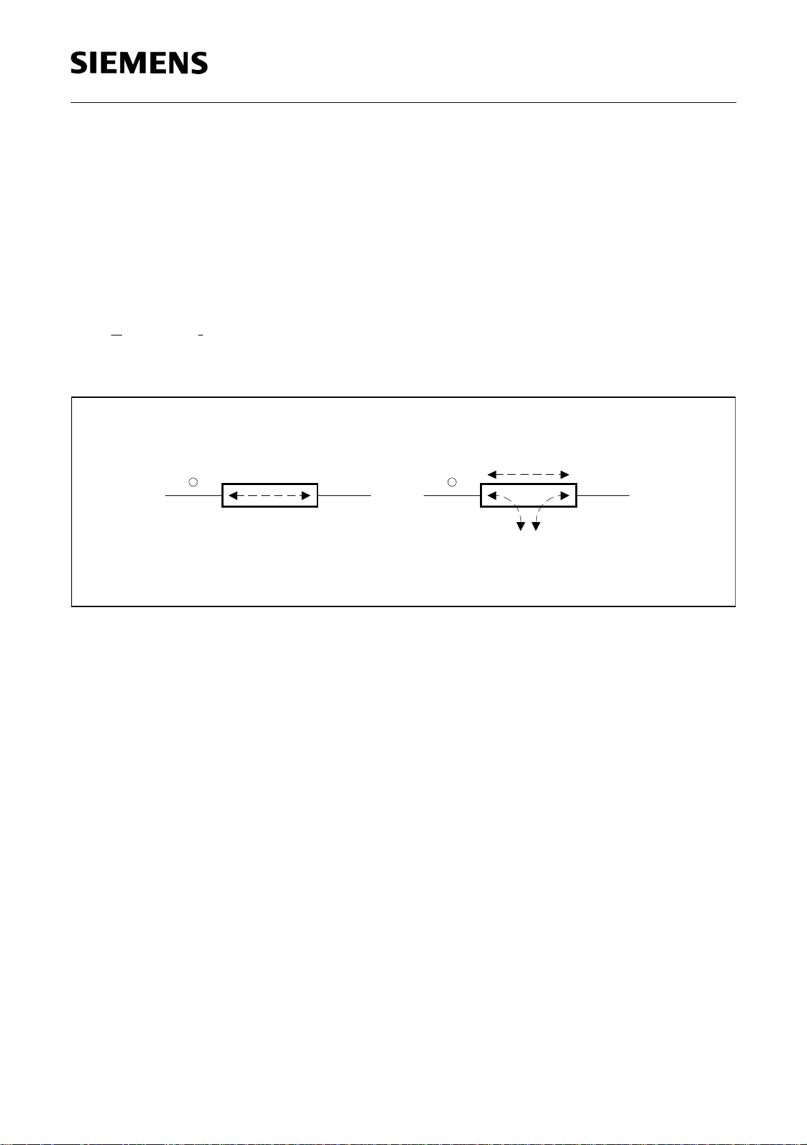
1 Overview
The PSB 21911, IEC-Q TE Version 5.2, is a specific derivative of the PEB 2091, IEC-Q
for terminal and small PBX applications. It features all necessary functions required for
NTs and terminal applications like PC add-on cards and terminal adapt ers .
In stand-alone mode the PSB 21911 IEC-Q TE Version 5.2 can be used fully pin
compatible to IEC-Q V4.4 and former vers ions. In µP mode it offers a parallel or serial
microprocessor interface.
The P
rocessor Interface (PI) of the IEC-Q TE V 5.2 establishes the access of a
microprocessor between U-interface and IOM-2. It’s main function is illustrated in
figure 1
.
FSC
R
IOM -2
R
IOM -2
UU
PI
ITS10193
Figure 1 Stand-Alone Mode (left) and µP Mode (right)
In µP mode B ch annels, D channel, C/I codes and Monitor commands can either be
passed between the U-transceiver and IOM-2 directly, or they can be looped through the
µP via the PI. Any selection of "passed" or "looped" channels can be programmed via a
control register.
The µP-interface mode is en abl ed by setting the pin PMODE to "1". This pin w as not to
be connected in older versions of the IEC-Q. Its internal pul l down resistor selects the
stand-alone mode, if the pin is left open.
In stand-alone mode the IEC-Q TE is controlled exclusively vi a the IOM-2 interface and
mode selection pins.
Semiconductor Group 8 11.97
Page 9
ISDN Echo cancellation Circuit fo r Terminal
PSB 21911
Applications
IEC-Q TE
Version 5.2 CMOS
1.1 Features
• ISDN U-transceiver with IO M-2 and optional m icro-
processor interface
• Compatible to NT modes and TE mode of
PEB 2091 IEC-Q V5.1
• Perfectly suited for terminal and TA applications
• U-interface (2B1Q) conform to ANSI T1.601, ETSI
ETR 080 and CNET ST/LAA/ELR/DNP/822:
– Meets all transmission requirements on all ANSI,
ETSI and CNET loops with margin
– Conform to British Telecom’s RC7355E
– Compliant with ETSI 10ms micro interruptio ns
• IOM-2 interface for connection of e.g. ISAC-S,
SICOFI-2/4TE, ARCOFI, ITAC, HSCX-TE, ISAR,
IPAC, 3PAC
• Pin compatible to version 4.4 in the P-LCC-44
package
P-LCC-44
T-QFP-64
In µP mode:
• Parallel or serial microprocessor interface and watchdog
• µP access to B-channels, D-channel and intercommunication channels
• µP access to IOM-2 Monitor-channels and C/I-channels
• Adjustable microcontroller clock source between 0.96MHz and 7.68MHz
• Selection between Bit clock (BCL) and Data clock (DCL)
• Supports synchronization of bas esta tions in cordl ess app licatio ns (e.g . RITL)
• Supports D-channel arbitration with ELIC linecard (e.g. PBX)
In all modes:
• Single 5 Volt power supply
• Low power CMOS technology with power down mode
Semiconductor Group 9 11.97
Page 10
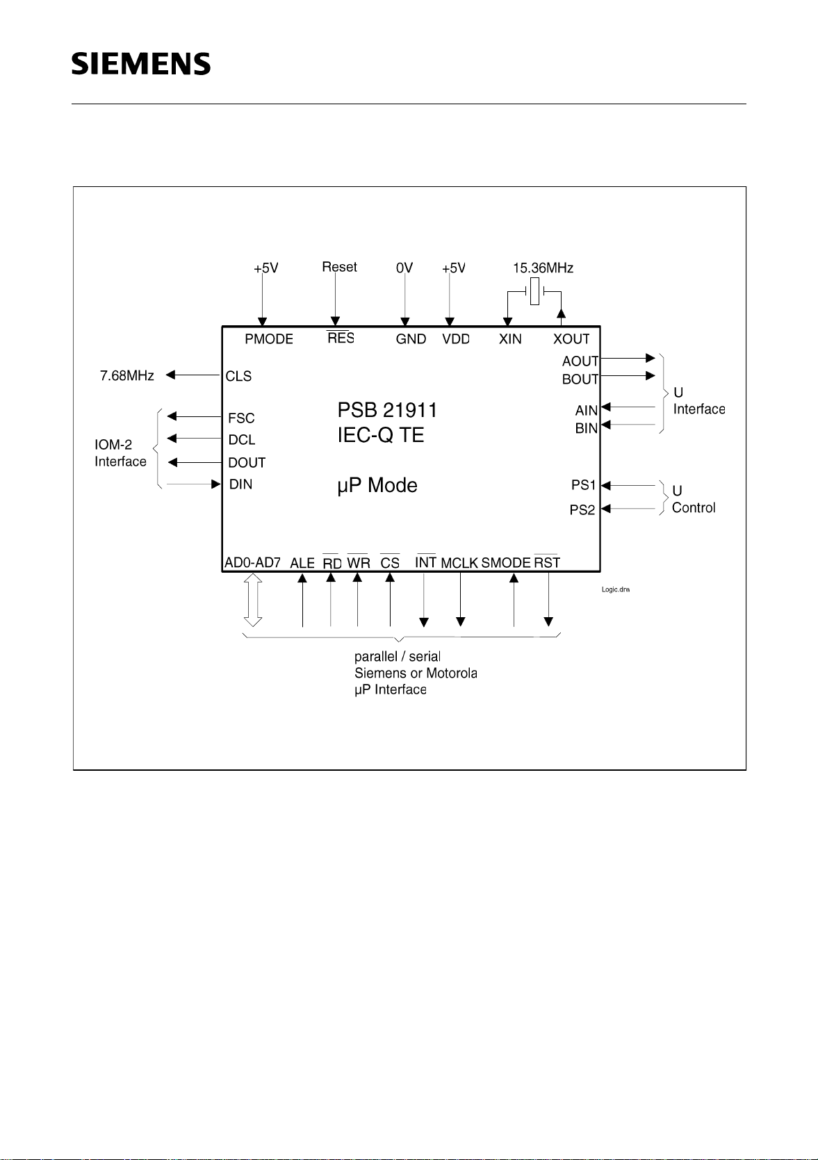
1.2 Logic Symbol µP Mode
PSB 21911
PSF 21911
Logic Symbol µP Mode
Figure 2 Logic Symbol µP Mode
Semiconductor Group 10 11.97
Page 11
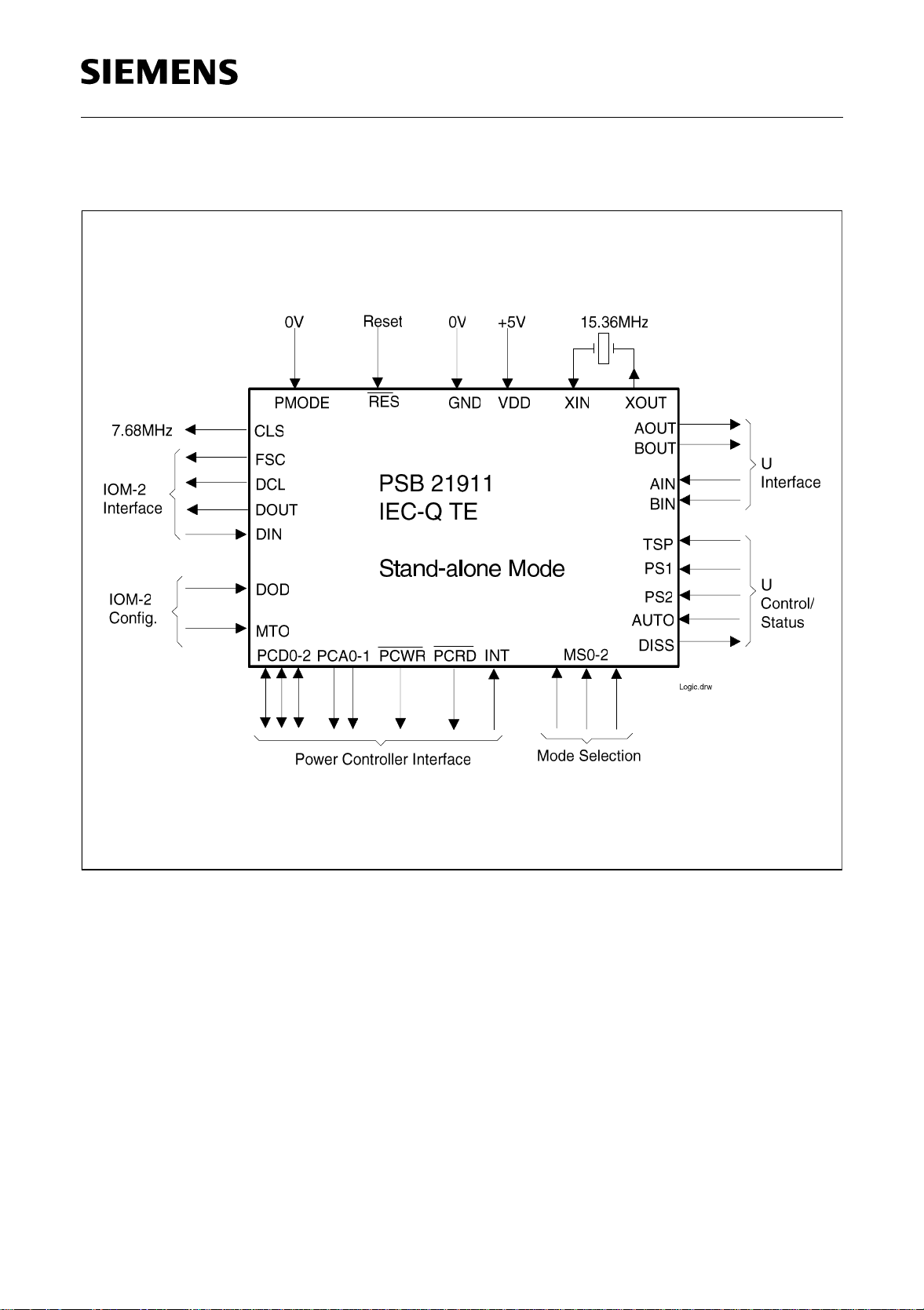
1.3 Logic Symbol Stand-Alone Mode
PSB 21911
PSF 21911
Logic Symbol Stand-Alone Mode
Figure 3 Logic Symbol Stand-Alone Mode
Semiconductor Group 11 11.97
Page 12
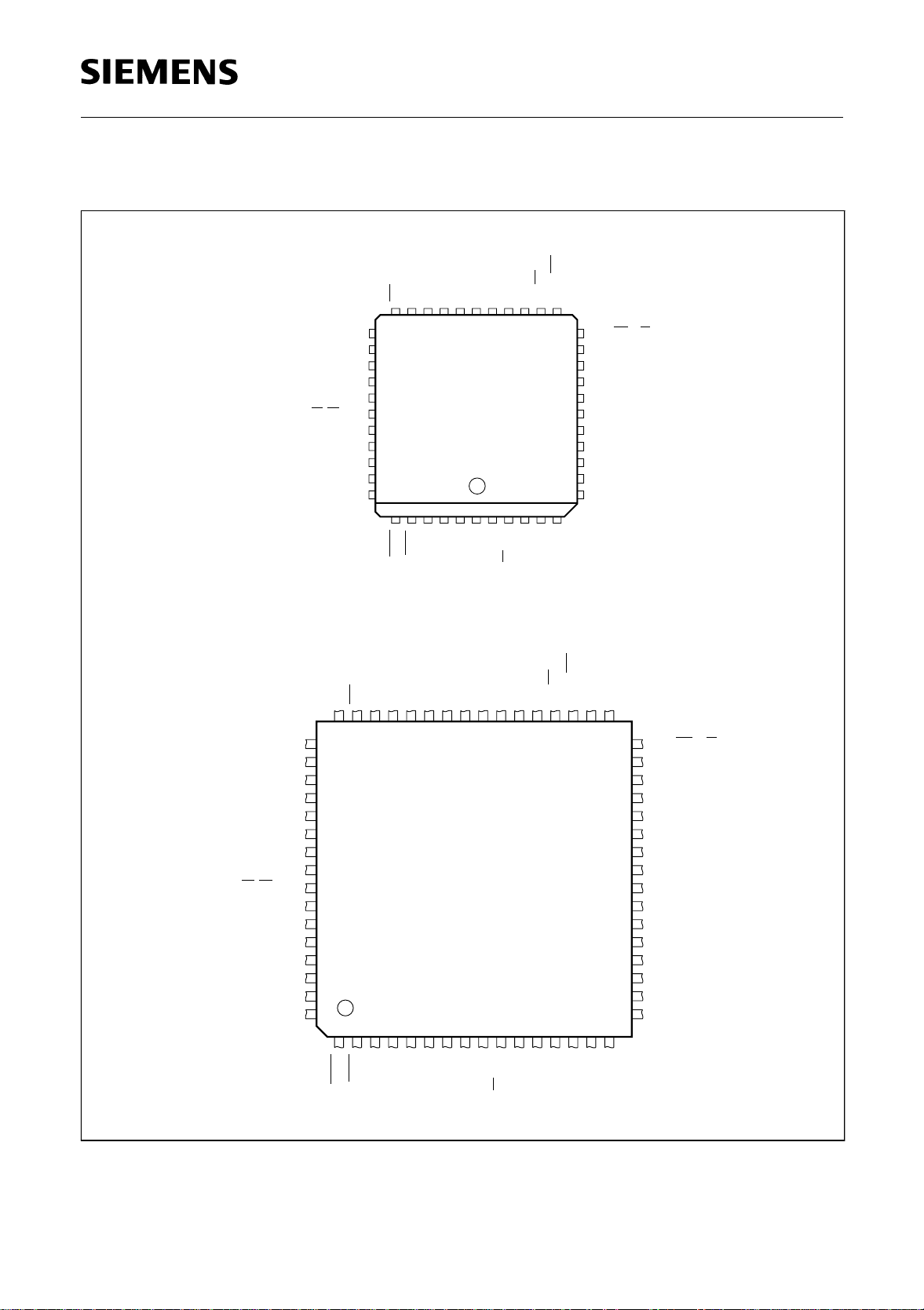
1.4 Pin Configuration
A3/MS0
DS/RD/MTO
CDOUT/A2/MS1
CDIN/A1/MS2
MCLK/DISS
D6/AD6/PCA1
D5/AD5/PCA0
TP
FSC
DCL
CLS
RES
DOUT
29
30
31
32
33
34
35
36
37
38
39
40 41 42 43 44
DIN
GNDd/D7/AD7
GNDd/A0/SMODE
GNDd
PS2
2425262728 23 22 21 20 19 18
IEC-Q TE
PSB 21911
123456
PS1
TP1/CCLK/ALE
INT/INT
AUTO/RSTAOUT
17
16
15
14
13
12
11
10
DOD/WR/R/W
GNDa2
AIN
BIN
V
DDa2
PMODE
XIN
XOUT
V
9
REF
V
8
DDa1
V
7
DDa1
PSB 21911
PSF 21911
Pin Configuration
N.C.
TP
FSC
DCL
CLS
A3/MS0
N.C.
DS/RD/MTO
CDOUT/A2/MS1
CDIN/A1/MS2
MCLK/DISS
D6/AD6/PCA1
D5/AD5/PCA0
N.C.
N.C.
49
50
51
52
53
54
55
56
57
58
59
60
61
62
63
64
N.C.
48 47
RES
21
DOUT
AD1/D1/PCD1
AD2/D2/PCD2
AD3/D3/PCRD
AD4/D4/PCWR
GNDd/D7/AD7
DIN
AD0/D0/PCD0
GNDd/A0/SMODE
N.C.
IEC-Q TE
PSB 21911
DDd
V
GNDd
N.C.
V
DDd
PS2
BOUT
CS/TSP
PS1
GNDa1
TP1/CCLK/ALE
ITP10290
AUTO/RST
INT/INT
N.C.
N.C.
3334353637383940414243444546
32 DOD/WR/R/WN.C.
31
30
29
28
27
26
25
24
23
22
21
20
19
18
17
161514131211109876543
N.C.
GNDa2
AIN
BIN
N.C.
V
DDa2
N.C.
PMODE
XIN
XOUT
V
REF
N.C.
V
DDa1
V
DDa1
N.C.
ITP10217
AOUT
AD1/D1/PCD1
AD2/D2/PCD2
AD3/D3/PCRD
AD4/D4/PCWR
AD0/D0/PCD0
N.C.
DDd
V
DDd
V
N.C.
N.C.
V
CS/TSP
DDd
BOUT
GNDa1
N.C.
Figure 4 Pin Configuration P-LCC-44 and T-QFP-64 Package (top view)
Semiconductor Group 12 11.97
Page 13
PSB 21911
PSF 21911
Pin Definitions and Functions
1.5 Pin Definitions and Functions
The following tables group the pins according to their functions. They include pin name,
pin number, type and a brief description of the function.
Pin No. Symbol I/O Function
P-LCC-44 T-QFP64
Standalone
µP
mode
Power Supply Pins
1, 2 7, 8, 12
V
DDd
V
DDd
I5 V
±
5% digital supply voltage
5 14 GNDa1 GNDa1 I 0 V analog
7, 8 18, 19
921
V
V
DDa1
REF
V
V
DDa1
REF
I5 V ± 5% analog supply voltage
O
V
pin to buffer internally generated
REF
voltage with capacitor 100 nF vs GND
13 26
V
DDa2
V
DDa2
I5 V ± 5% analog supply voltage
16 30 GNDa2 GNDa2 I 0 V analog
23 41 GNDd G NDd I 0 V digital
Mode Selection Pins
310TSP I
Single Pulse Test Mode
CS
18 35 AUTO I
RST
I
O
For activation refer to table 3 on
page 27. When active, alternating
2.5 V pulses are issued in 1.5 ms
intervals. Tie to GND if not used.
Chip Select
(Multiplexed, demultiplexed and serial
modes): Low active.
Auto EOC Mode
Selection between auto- and
transparent mode for EOC channel
processing. (Automode = (1))
Reset output
(Multiplexed, demultiplexed and serial
modes): Low active.
Semiconductor Group 13 11.97
Page 14

Pin Definitions and Functions
Pin No. Symbol I/O Function
PSB 21911
PSF 21911
P-LCC-44 T-QFP64
24 43 GNDd I
25 44 GNDd I
Standalone
µP
mode
A0 I
SMODE I
D7 I/O
AD7 I/O
GNDd
Must be connected t o GNDd in sta ndalone mode.
Address Bus Pin
(Demultiplexed mode)
Serial Mode Pin:
serial mode, SMODE = 0 enables the
multiplexed mode.
GNDd
Must be connected t o GNDd in sta ndalone mode.
Data Bus Pin
(Demultiplexed modes)
Address Data Bus Pin
SMODE = 1 selects
not used I (Serial mode) tie to GND.
33 55 MS0 I
not used I (Multiplexed mode) tie to GND.
A3 I
not used (Serial mode) tie to GND.
35 58 MS1 I
not used I (Multiplexed mode) tie to GND.
A2 I
CDOUT O
(Multiplexed mode)
Mode Selection 0
refer to table 2 on page 26.
Address Bus Pin
(Demultiplexed modes).
Mode Selection 1
refer to table 2 on page 26.
Address Bus Pin
(Demultiplexed modes).
Controller Data Out
CCLK determines the data rate.
CDOUT is "high Z" if no data is
transmitted.
Semiconductor Group 14 11.97
Page 15
Pin Definitions and Functions
Pin No. Symbol I/O Function
PSB 21911
PSF 21911
P-LCC-44 T-QFP64
36 59 MS2 I
28 47 RES
Power Controlle r Interface P in s
Standalone
µP
mode
not used I (Multiplexed mode) tie to GND.
A1 I
CDIN I
RES I
Mode Selection 2
refer to table 2 on page 26.
Address Bus Pin
(Demultiplexed modes).
Controller Data In
CCLK determines the data rate.
Reset
Low active, must be (0) at least for
10 ns.
Refer also to table 3 on page 27 for test
modes invoked with this pin.
(Serial mode)
44 5 PCD0 I/O
(PU)
AD0 I/O
D0 I/O
not used I (Serial mode) tie to GND.
43 4 PCD1 I/O
(PU)
AD1 I/O
D1 I/O
Data Bus 0 of Power Controller
Interface
internal pull-up.
Address/Data Bus Pin
(Multiplexed mode)
Data Bus Pin
(Demultiplexed modes)
Data Bus 1 of Power Controller
Interface
Internal pull-up.
Address/Data Bus Pin
(Multiplexed mode)
Data Bus Pin
(Demultiplexed modes)
not used I (Serial mode) tie to GND.
Semiconductor Group 15 11.97
Page 16
Pin Definitions and Functions
Pin No. Symbol I/O Function
PSB 21911
PSF 21911
P-LCC-44 T-QFP64
42 3 PCD2 I/O
39 62 PCA0 O
Standalone
µP
mode
(PU)
AD2 I/O
D2 I/O
not used I (Serial mode) tie to GND.
D5 I/O
AD5 I/O
Data Bus 2 of Power Controller
Interface
Internal pull-up.
Address/Data Bus Pin
(Multiplexed mode)
Data Bus Pin
(Demultiplexed modes)
Address bus 0 of Power Controller
Interface
Data Bus Pin
(Demultiplexed modes)
Address Data Bus Pin
(Multiplexed mode)
.
not used I (Serial mode) tie to GND.
38 61 PCA1 O
D6 I/O
AD6 I/O
not used I (Serial mode) tie to GND.
41 2 PCRD
D3 I/O
AD3 I/O
not used I (Serial mode) tie to GND.
O
Address bus 1 of Power Controller
Interface
Data Bus Pin
(Demultiplexed modes)
Address Data Bus Pin
(Multiplexed mode)
Power Controller Bus Read Request
Low active.
Data Bus Pin
(Demultiplexed modes)
Address/Data Bus Pin
(Multiplexed mode)
Semiconductor Group 16 11.97
Page 17

Pin Definitions and Functions
Pin No. Symbol I/O Function
PSB 21911
PSF 21911
P-LCC-44 T-QFP64
40 1 PCWR O
19 36 INT I
Standalone
µP
mode
D4 I/O
AD4 I/O
not used I (Serial mode) tie to GND.
INT
O
Power Controller Bus Write Request
Low active.
Data Bus Pin
(Demultiplexed modes)
Address/Data Bus Pin
(Multiplexed mode)
Interrupt
Change-sensitive. After a change of
level has been detected the C/I code
“INT” will be issued on IOM. Tie to
GND if not used.
Interrupt Line
(Multiplexed, demultiplexed and serial
modes): Low active
.
37 60 DISS O
MCLK O
21 38 PS1 PS1 I
22 39 PS2 PS2 I
Disable Power Supply
This pin is set to ’1’ after receipt of
MON-0 LBBD in EOC auto-mode.
Microprocessor Clock Output
(Multiplexed, demultiplexed and serial
modes): provided with four
programmable clock rates: 7.68 MHz ,
3.84 MHz, 1.92 MHz and 0.96 MHz.
Power Status 1 (prima ry )
’1’ indicates primary pow er supply ok.
The pin level is identical to the
overhead bit ’PS1’ value.
Power Status 2 (secondary)
’1’ indicates secondary power supply
ok. The pin level is identical to the
overhead bit ’PS2’ value.
.
Semiconductor Group 17 11.97
Page 18
Pin Definitions and Functions
Pin No. Symbol I/O Function
PSB 21911
PSF 21911
P-LCC-44 T-QFP64
Miscellaneous Function Pins
10 22 XOUT XOUT O
11 23 XIN XIN I
17 32 DOD I
Standalone
µP
mode
WR
Crystal OUT
To connect 15.36-MHz crystal.
Leave open if not used.
Crystal IN
To connect 15.36-MHz crystal or
external 15.36-MHz clock.
DOUT Open Drain
Select open drain with DOD = (1)
(external pull-up resi sto r requir ed) and
tristate with DOD = (0). See also
table 4 on page 27.
I
Write
(Siemens/Intel multiplexed and
demultiplexed modes): indicates a
write operation, active low.
R/W
not used I (Serial mode) tie to GND.
29 51 TP TP I
20 37 TP1 I
ALE I
I
(PD)
(PD)
Read/Write
(Motorola demultiplexed mode):
indicates a read (high) or write (low)
operation.
Test Pin
Not available to user. Do not connect.
Internal pull-down resistor.
Test Pin 1
Not available to user. Do not connect.
Internal pull-down resistor.
Address Latch Enable
(Multiplexed mode): In the Siemens/
Intel µP interface modes a high
indicates an address on the AD0..3
pins which is latched with the falling
edge of ALE (see also page 39).
Semiconductor Group 18 11.97
Page 19

Pin Definitions and Functions
Pin No. Symbol I/O Function
PSB 21911
PSF 21911
P-LCC-44 T-QFP64
Standalone
µP
mode
ALE I
CCLK I
32 54 CLS CLS O
12 24 PMODEPMODE I
(PD)
Address Latch Enable
(Demultiplexed mode): ALE tied to
GND selects the Siemens/Intel type.
ALE tied to VDD selects the Motorola
type.
Controller Data Clock
(Serial mode): Shifts data from (1) and
to (0) the device.
Clock Signal
A 7.68MHz clock, sync hronous to the
U-interface, is provided on this pin.
Processor Interface Enable
Setting PMODE to “1“ enables the
Processor Interface. Tie to GND or do
not connect to select stand-alone
mode. Internal pull down.
34 57 MTO I
RD
DS
not used I (Serial mode) tie to GND.
6, 9, 11,
15, 20, 25,
27, 31, 33,
34, 40, 48,
49, 50, 51,
63, 64
not
used
not used Leave open for future compatibility.
(PD)
I
I
Monitor Procedure Time-Out
Disables the internal 6 ms Monitor
time-out when set to (1). Internal pulldown resistor.
Read
(Siemens/Intel multiplexed and
demultiplexed modes): indicate s a
read operation, active low.
Data Strobe
(Motorola demultiplexed mode):
indicates a data transfer, active low.
Semiconductor Group 19 11.97
Page 20

Pin Definitions and Functions
Pin No. Symbol I/O Function
PSB 21911
PSF 21911
P-LCC-44 T-QFP64
®
IOM
-2 Pins
Standalone
µP
mode
31 53 DCL DCL O
30 52 FSC FSC O
26 45 DIN DIN I
Data Clock
Data clock output 512 or 1536 kHz
(table 2 on page 26). In µ P mode this
pin can be programmed to deliver a bit
clock (256 or 768 kHz).
Frame Synchronization Clock
The start of the B1-channel in ti me-slot
0 is marked. FSC = (1) for one DCLperiod indicates a superframe marker.
FSC = (1) for at least two DCL-periods
marks a standard frame.
Data In
Input of IOM-2 data synchronous to
DCL-clock (Data upstream direction).
27 46 DOUT DOUT O
U-Interface Pins
15 29 AIN AIN I
14 28 BIN BIN I
6 16 AOUT AOUT O
4 13 BOUT BOUT O
PU: internal pull-up resistor
Data Out
Output of IOM-2 data synchronous to
DCL-clock. Open drain or tristate
depending on bit/pin DOD (Data
Downstream direction).
Differential U-Interface Input
Connect to hybrid.
Differential U-Interface Input
Connect to hybrid.
Differential U-Interface Output
Connect to hybrid.
Differential U-Interface Output
Connect to hybrid.
PD: internal pull-down resistor
Semiconductor Group 20 11.97
Page 21
PSB 21911
PSF 21911
Microprocessor Bus Interface (Overview)
1.6 Microprocessor Bus Inte rface (Overview )
The table below gives an overview of the different microprocess or bus m odes.
Table 1 Microprocessor Bus Interface
Pin number Stand-alone
Symbol in processor mode
mode
P-LCC44T-QFP
64
Siemens/
Intel
multiplexed
Siemens/
Intel
demultiplexed
Motorola
demultiplexed
Serial
12 24 PMODE = 0 PMODE = 1
455PCD0AD0D0D0n.c.
434PCD1AD1D1D1n.c.
423PCD2AD2D2D2n.c.
41 2 PCRD
40 1 PCWR
AD3D3D3n.c.
AD4D4D4n.c.
39 62 PCA0 AD5 D5 D5 n.c.
38 61 PCA1 AD6 D6 D6 n.c.
25 44 GNDd AD7 D7 D7 n.c.
19 36 INT INT
INT INT INT
24 43 GNDd SMODE=0 A0 A0 SMODE=1
36 59 MS2 n.c. A1 A1 CDIN
35 58 MS1 n.c. A2 A2 CDOUT
33 55 MS0 n.c. A3 A3 n.c.
20 37 TP1 ALE ALE=0 ALE=1 C C LK
34 57 MTO RD
17 32 DOD WR
310TSP CS
RD DS n.c.
WR R/W n.c.
CS CS CS
37 60 DISS MCLK
18 35 AUTO RST
Semiconductor Group 21 11.97
Page 22
PSB 21911
PSF 21911
System Integration
1.7 System Integration
Due to the IOM-2 interface the IEC-Q TE can be combined with a variety of other devices
to fit in numerous applications. This chapter only shows some typical applications of the
IEC-Q TE.
1.7.1 ISDN PC Adapter Card
An ISDN adapter card which supports the U-interface may be realized using the
IEC-Q TE together with the PSB 2113 3PAC (
and two B-channel HDLC controllers. Optionally, a PSB 2132 SICOFI2-TE can be
connected to provide two POTS interfaces. If an S-interface is required, the PSB 2115
IPAC can be used instead of the 3PAC.
figure 5
). The 3PAC provides a D-channel
Figure 5 ISDN PC Adapter Card
Semiconductor Group 22 11.97
Page 23
PSB 21911
PSF 21911
System Integration
1.7.2 ISDN Stand-Alone Terminal with POTS Interface
The IEC-Q TE can be integrated in a microcontroller based stand-alone terminal
(figure 6) that is connected to the communications interface of a PC. The PSB 2132
SICOFI-TE enables connect ion of analog terminals (e.g. telepho nes or fax) to its dual
channel POTS interface.
Figure 6 ISDN Stand-Alone Terminal with POTS Interface
Semiconductor Group 23 11.97
Page 24
PSB 21911
PSF 21911
System Integration
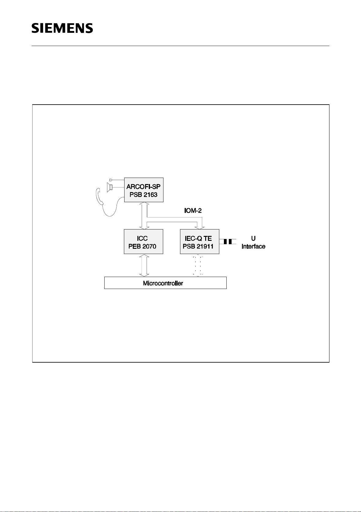
1.7.3 ISDN Feature Phone
An ISDN feature phone with U-interface can be built using the IEC-Q TE together with
the ARCOFI-SP and the ICC.
Figure 7 ISDN Feature Phone
Semiconductor Group 24 11.97
Page 25
PSB 21911
PSF 21911
System Integration
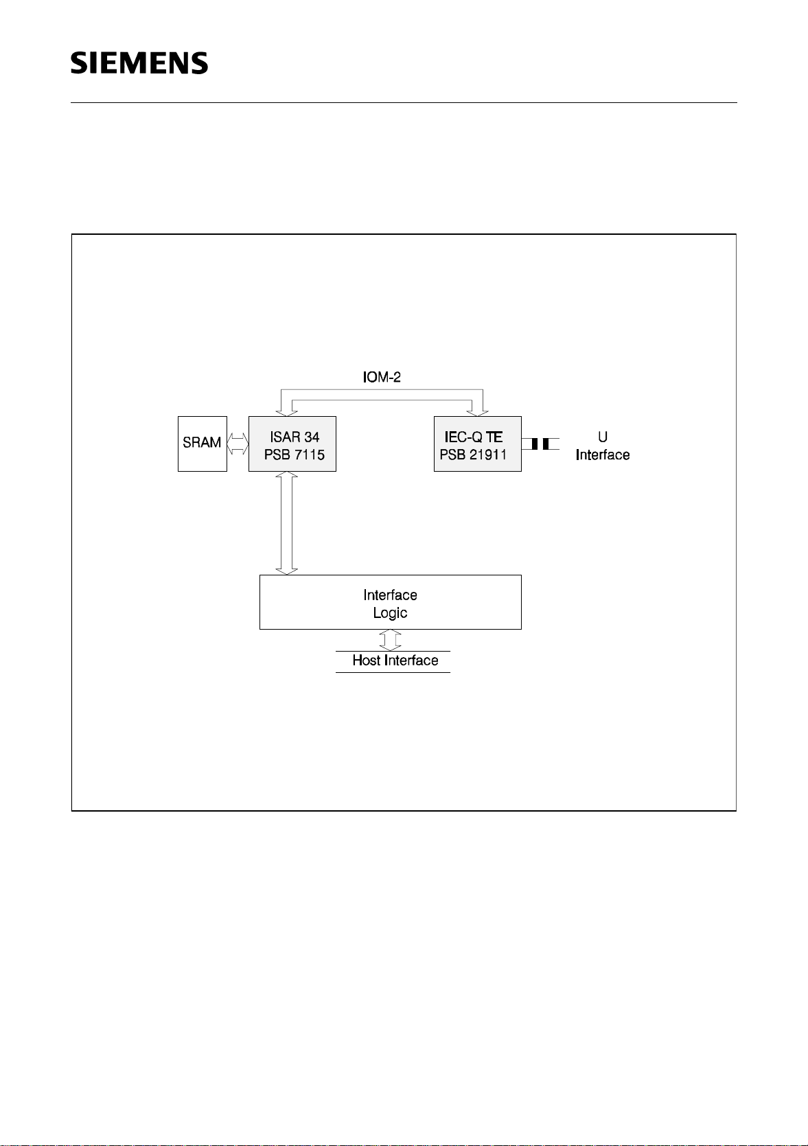
1.7.4 ISDN-Modem PC Card
The combination of the IEC-Q TE and a PSB 7115 I SAR 34 allows to build an ISDNmodem PC card .
Figure 8 ISDN-Modem PC Card
Semiconductor Group 25 11.97
Page 26
PSB 21911
PSF 21911
Operating Modes
2 Functional Description
2.1 Operating Modes
The default configuration after pow er-on or external reset depends on t he state of the
PMODE pin. The cases µP mode and stand-alone mode have to be distinguished:
µP mode (
PMODE
= VDD)
In µP mode a microprocessor inte rface gives access t o the IOM-2 channel r egi st ers as
well as configuration registers. The operating mode is selected via bits STCR:MS0-MS2
according to
table 2
. The STCR register is described on page 119.
Test modes Send Single Pulses, Quiet Mode or Data Through are invoked via the
corresponding C/I channel command (page 75) or via bits STCR:TM1-2 (
Stand-alone mode (
PMODE
= GND)
table 3
).
In stand-alone mode the operating mode is selected via pin strapping according to
table 2
. It is possible to change the mode of a device during operation (e.g. for test
purposes) if the mode change is followed by a reset.
The test modes Send Single Pulses (SSP), Quiet Mode (QM) and Data Through (DT)
are invoked via the corresponding C/I channel command (page 75) or via pins RES
TSP (
table 3
).
and
Table 2 Modes of Operation (µP and Stand-Alone Mode)
Mode Selection Output Pins U
Synchronized
Mode
NT 0 0 0 512 7680
NT 1 0 0 512 7680
NT-Auto 0 0 1 512 7680
TE 0 1 0 1536 7680
TE 1 1 0 1536 7680
Bit/Pin
MS2
Bit/Pin
MS1
Bit/Pin
MS0
DCL
OUT
CLS
OUT
2)
2)
2)
2)
2)
Superframemarker
no
yes
no
no
yes
1)
reserved others
1)
Notes:
Semiconductor Group 26 11.97
1 DCL-period high-phase of FSC at superframe position
2 DCL-periods high-phase of FSC at normal position
2)
CLS-clock signal not available while device is in power-down
Page 27
Table 3 Test Modes
PSB 21911
PSF 21911
Operating Modes
Test-Mode
Master-Reset
1)
Send Single-Pulses
Data-Through
3)
2)
Bit TM1/
Pin RES
00
11
01
Bit TM2/
Pin TSP
Normal 1 0
1)
Used for Quiet Mode and Return Loss measurements
2)
Used for Pulse Mask measurements
3)
Used for Insertion Loss, Power Spect ral Density and Tot al Power measurements
Table 4 DOUT Driver Modes
Mode Pin
RES
Pin
1)
TSP
2)
Pin /
Bit
DOD
Pin DOUT Output Driver
Value DOUT in
active time
slot
DOUT in
passive time
slot
Pin-Reset 0 0 x 0 low int. p u ll-up
1 int. pull-up
Normal
(Tristate)
Normal
3)
(Open Drain
1)
In stand-alone mode and µP mode
2)
Only in stand-alone mode. In µP mode the output driver of pin DOUT is selected via bit DOD in the ADF2
regist er
3)
External pull-up resistors required (typ.1 kΩ)
)
1000low high Z
1high
1010low floating
1floating
Semiconductor Group 27 11.97
Page 28
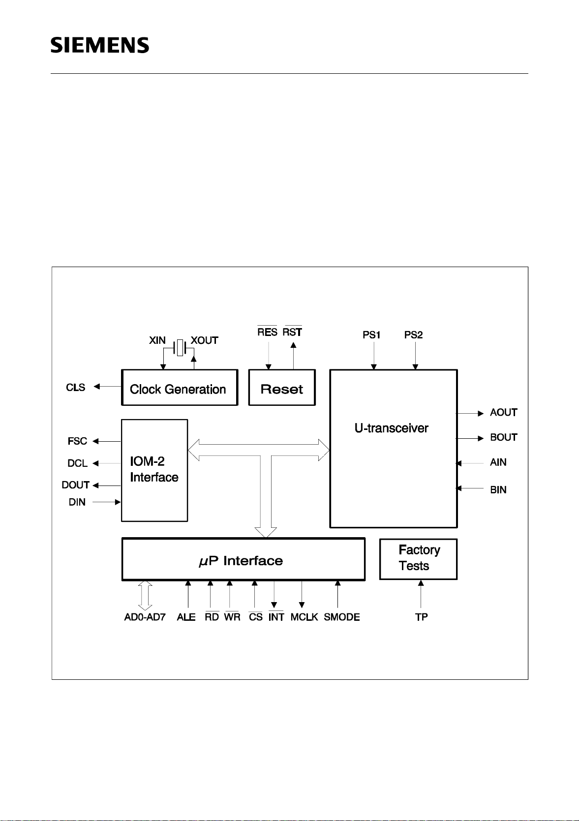
2.2 Devi ce Arch itecture
In µP mode the following interfaces and functional blocks are used:
• IOM-2 interface see pp. 30
• Microprocessor interface pp. 39, 81, 112
• U-transceiver pp. 40
• Clock G ener ation pp. 111
• Reset pp. 93
• Factory Test Unit
PSB 21911
PSF 21911
Device Architecture
Figure 9 IEC-Q TE Device Architecture (µP Mode)
Semiconductor Group 28 11.97
Page 29
PSB 21911
PSF 21911
Device Architecture
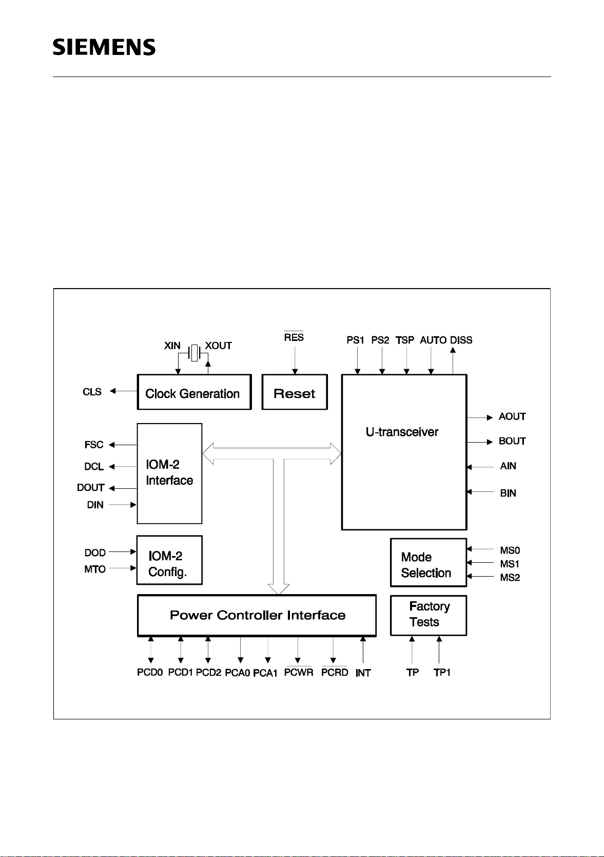
In stand-alone mode the following interfaces and functional bloc ks are use d:
• Mode Selection see pp. 26
• IOM-2 interface pp. 30
• IOM-2 configuration pp. 36, 38
• U-transceiver pp. 40
• Clock Generation pp. 111
• Reset pp. 93
• Power Controller Interface pp. 94
• Factory Test Unit
Figure 10 IEC-Q TE Device Architecture (Stand-Alone Mode)
Semiconductor Group 29 11.97
Page 30
PSB 21911
PSF 21911
IOM®-2 Interface
2.3 IOM®-2 Interface
The IOM-2 interface is used to interconnect telecommunication ICs. It provides a
symmetrical full-dupl ex communicat ion link, containing us er dat a, control/program ming
and status channels. The structure used follows the 2B + 1D-channel structure of ISDN.
The ISDN user data rate of 144 kbit/s (B1 + B2 + D) is transmitted in both directions over
the interface.
The IOM-2 interface is a generalization and enhancement of the IOM-1 interface.
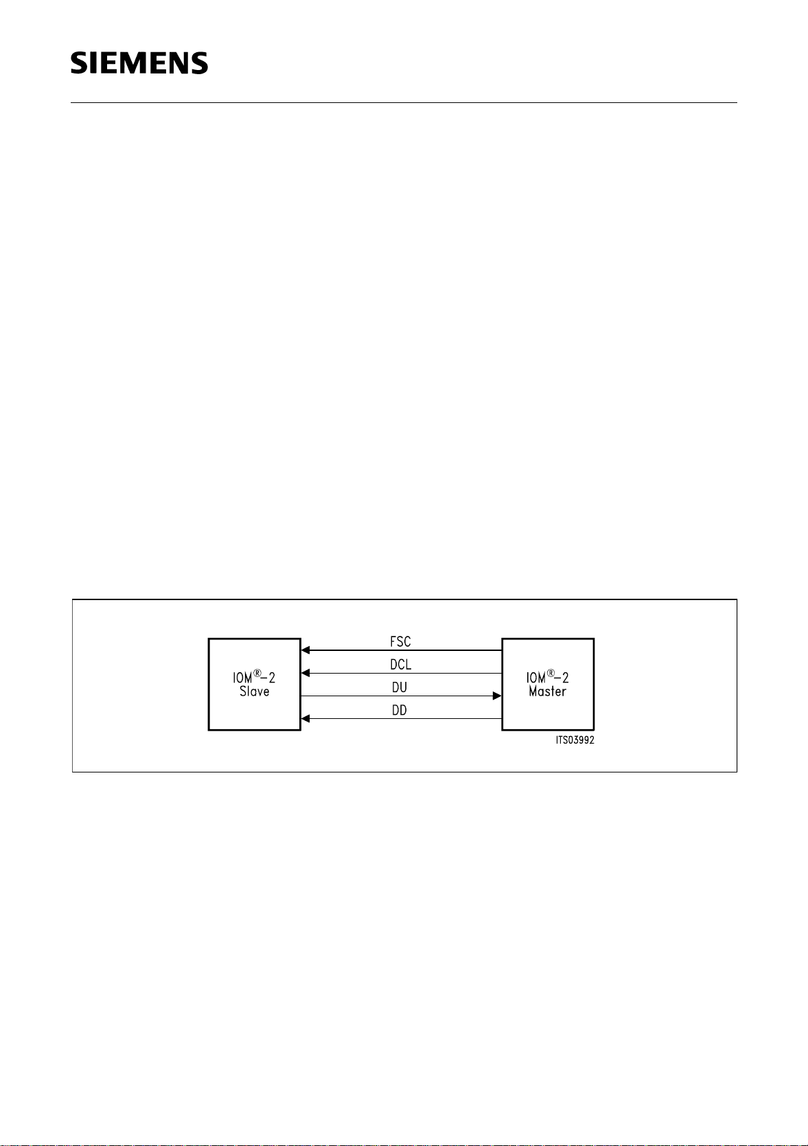
®
2.3.1 IOM
The IOM-2 interface comprises two clock lines for synchronization and two data lines.
Data is carried over Data Upstream (DU) and Data Downstream (DD) signals. The
downstream and upstream di rection are always defined with respect to the exchan ge.
Downstream refers to information flow from the exchange to the subscriber and
upstream vice versa respectively. The IOM-2 Interface Specification describes open
drain data lines with external pull-up resistors. However, if operation is logically point-topoint, tristate operation is possible as well.
-2 Frame Structure
The data is clocked by a Data Clock (DCL) that operates at twice the data rate. Frames
are delimited by an 8-kHz Frame Synchronization Clock (FSC). Incoming data is
sampled on every second falling edge of the DCL cl ock.
Figure 11 IOM®-2 Clocks and Data Lines
Within one FSC period 32 bit or 96 bit are transmitted, corresponding to DCL
frequencies of 512 kHz or 1.536 MHz.
Two optimized IOM-2 timing modes exist:
– NT mode for NT1 applications
– TE mode for terminal and intelligent NT applications
Semiconductor Group 30 11.97
Page 31

PSB 21911
PSF 21911
IOM®-2 Interface
NT or TE mode is selected via pins MS0-2 in stand-alone m ode and via bits M S0-2 in
µP mode. Both the NT and TE mode utilize the same basic frame and clocking structure,
but differ in the number and usage of the individual channels.
®
Figure 12 Basic Channel Structure of IOM
Each frame consists of
-2
• two 64 kbit/s channels B1 and B2
• the Monitor channel for transferring maintenance informa tion
• two bits for the 16 kbit/s D-channel
• four command/indication (C/I) bits for controlling of layer-1 functions (U- and Stransceiver).
• two bits MR and MX for the handshake procedure in the Monitor channel
2.3.1.1 TE Mode Frame Structure
In TE mode the IEC- Q T E provide s a data clock DCL with a frequency of 1536 kHz. As
a consequence the IOM-2 interface provides three channels each with a nominal data
rate of 256 kbit/s.
• Channel 0 contains 144 kbit/s (for 2B+D) plus Monitor and Command/Indication
channels for the layer-1 device.
• Channel 1 contains two 64-kbit/s intercommunication channels plus Monitor and
Command/Indication channels for other IOM-2 devices.
• Channel 2 is used for IOM bus arbitration (access to the TIC bus). Only the Command/
Indication bits are used in channel 2.
The IOM-2 signals are:
DIN, DOUT 768 kbit/s
DCL 1536 kHz output
FSC 8 kHz output
Semiconductor Group 31 11.97
Page 32

PSB 21911
PSF 21911
IOM®-2 Interface
125 µs
FSC
R
Channel 0
IOM
DD B1 B2 MON0 C/I0 IC1 IC2 MON1 C/I1
IOM
R
Channel
1 Channel
C/I1MON1IC2IC1C/I0MON0B2B1DU
IOM
R
2
C/I2
C/I2
B1
B1
ITD09787
Figure 13 Definition of the IOM®-2 Frame in TE Mode
C/I0 in IOM
–
®
-2 Channel 0:
DU / DD D D C/I4 C/I3 C/I2 C/I1 MR MX
D:
C/I:
two bits for the 16 kbit/s D-channel
The four command/indication (C/I) bits are used for control of the U-
transceiver (activation/deactivation and additional control
functions).
MR, MX:
C/I1 in IOM
–
®
two bits MR and MX for the handshake in the Monitor channel 0
-2 Channel 1:
DU / DD C/I6 C/I5 C/I4 C/I3 C/I2 C/I1 MR MX
C/I1 to C/I6
are used for control of a transceiver or an other device in IOM-2
channel 1 (activation/deactivation and additional control functions).
MR, MX:
Semiconductor Group 32 11.97
two bits MR and MX for handshake in the Monitor channel 1
Page 33

PSB 21911
PSF 21911
IOM®-2 Interface
C/I2 in IOM
–
®
-2 Channel 2:
DU 1 1 BAC TBA2 TBA1 TBA0 1 1
DD EES/GA/B1111
E:
BAC-bit
S/G-bit
D-echo bits
(Bus ACcessed). When the TIC bus is occupied the BAC-bit is low.
(Stop/Go), available to a connected HDLC controller to determine if
it can access the D-channel (S/G = 1: stop, S/G = 0: go).
A/B-bit
(available/blocked), supplementary bit for D-channel control.
(A/B = 1: D-channel available, A/B = 0: D-channel blocked).
TBA0-2:
TIC Bus Address
2.3.1.2 NT Mode Structure
In NT mode the IEC-Q TE provides a data clock DCL with a frequency of 512 kHz. As a
consequence the IOM-2 interface provides only one channel with a nominal data rate of
256 kbit/s.
• Channel 0 contains 144 kbit/s (for 2B+D) plus Monitor and Command/Indication
channels.
The IOM-2 signals are:
DIN, DOUT 256 kbit/s
DCL 512 kHz output
FSC 8 kHz output
µs125
FSC
R
IOM Channel 0
DD
DU
B1 B2 MONITOR D C/I
B1 B2 MONITOR D
C/I
M
RMX
M
M
RX
ITD09788
Figure 14 Definition of the IOM®-2 Frame in NT Mode
Semiconductor Group 33 11.97
Page 34

PSB 21911
PSF 21911
IOM®-2 Interface
2.3.2 IOM®-2 Command / Indication Channels
The Command/Indication chan nels carry real-time control and status information over
the IOM-2 interface.
C/I Channel 0
C/I channel 0 (C/I0) is available in both operational modes (NT and TE mode). The
channel consists of four bits in each direction. Activation and deactivation of the Utransceiver is always controlled via the C/I0 channel. The C/I codes going to the Utransceiver are called “commands”, those originating from it are referred to as
“indications”. The C/I codes of the U-transceiver are listed and explained in chapter 2.5.8
on page 74.
stand-alone mode
In
3PAC, IPAC or ISAR.
the C/I0 channel is controlled by an external device, e.g. the ICC,
µP mode
In
microprocessor interfa ce. For a description on how to access the C/I0 channel via the
µP-interface please refer to chapter 2.6.3 on page 83.
C/I Channel 1
C/I channel 1 (C/I1) is only available in TE mode (DCL = 1.536 MHz). The channel
consists of six bits in each direction.
stand-alone mode
In
µP mode
In
the C/I0 channel ca n either be controlled by an external device or via the
the C/I1 channel is ignored by the U-transceiver.
it can be accessed via registers CIWI/U and CIRI/U (pag e 83).
Semiconductor Group 34 11.97
Page 35

PSB 21911
PSF 21911
IOM®-2 Interface
2.3.3 IOM®-2 Monitor Channel
The Monitor channel protocol is a handshake protocol used for programming and
monitoring devices in Monitor channel "0" or "1". These can include the on-chip Utransceiver of the IEC-Q TE as well as external devices connected to the IOM-2
interface.
The Monitor channel ope rates on an asynchro nous basis. While data tra nsfers on the
bus take place synchronized to frame sync, the flow of data is controlled by a handshake
procedure. For example: data is placed onto the Monitor channel and the MX bit is
activated. This data will be transmitted repeatedly once per 8-kHz frame until the transfer
is acknowledged via the MR bit.
Monitor Channel 0
Monitor channel 0 is available in both operational modes (NT and TE mod e). The Utransceiver is always controlled and monitored via Monitor channel 0. The Monitor
channel commands and indications of the U-trans ceiver are listed and explained on
page 5 1-61.
stand-alone mode
In
ICC, 3PAC, IPAC or ISAR.
µP mode
In
microprocessor interface. For a descr ipti on on how t o access the Monitor 0 channel via
the µP-interface please refer to chapter 2.6.4 on page 84.
Monitor Channel 1
Monitor channel 1 is only available in TE mode (DCL = 1.536 MHz). The channel
consists of six bits in each direction.
stand-alone mode
In
µP mode
In
external device (e.g. ARCOFI).
the Monitor channel can either be controlled by an external device or via the
it can be accessed via the microprocessor interface (page 83) to control an
the Monitor channel is controlled by an external device, e.g . the
the Monitor 1 channel is ignored by the U-transceiver.
Semiconductor Group 35 11.97
Page 36

PSB 21911
PSF 21911
IOM®-2 Interface
Monitor Procedure ’Timeout’
The U-transceiver offers an automatic reset (Monitor procedure “Timeout”) for the
Monitor routine. This reset function transfers the Monitor channel into the idle state (MR
and MX set to high) by issuing “EOM” (End of Message) after a timer has elapse d. As
an effect, unacknowledged Monitor messages sent by the U-transceiver are taken away
from the Monitor channel.
The U-transceiver checks for unacknowled ged Monitor messages every 5 m s. In case
the timer expires “EOM” will be issued. The U-transceiver does not repeat the message,
hence it will be lost.
In slow applications e.g. testing or evalution platforms this internal reset function may be
disabled by setting
– Pin MTO in stand-alone mode
– Bit ADF2:MTO in µP mode.
If Monitor Timeout is disabled, no restrictions regarding the time for completing a Monitor
transfe r e xi s ts.
Semiconductor Group 36 11.97
Page 37

PSB 21911
PSF 21911
IOM®-2 Interface
2.3.4 Activation/Deactivation of IOM®-2 Clocks
The IOM-2 clocks may be switched off if the U-transceiver is in state ’Deactivated’. This
reduces power consum ption to a minimum . In this deactivat ed state the cl ock lines are
low and the data lines are high. The power-down condition within the ’Deactivated’ state
will only be entered if no Monitor messages are pending on IOM-2.
For information on how to keep the IOM- 2 clocks a ctive in all states please refer to the
application note ’Providing Clocks in Deacti vate d State’ of 09.97.
deactivation procedure
The
is shown in
figure 15
. After detecting the code DI
(Deactivation Indi cation) the U-transce iver responds by transmitting D C (Deactivation
Confirmation) during s ubsequent frames and stops the timing signals after the fourth
frame.
a)
FSC
DI DI DI DI DI DI
DIN
DCDCDCDCDRDR
DOUT
Detail see Fig.b
b)
DCL
R
IOM -2 Interface
deactivated
R
IOM -2 Interface
deactivated
DIN
Figure 15 Deactivation of the IOM
The IOM-2 clocks a re
DC/ΙΙ/C Ι/C Ι/C
®
-2 Clocks
activated
automatically when the DIN line is pul led low or a line
ITD10292
activation is detected on the U-interface. If a PSB 2186 (ISAC-S TE) or PEB 2070 (I CC)
is connected to the IEC-Q TE via IOM-2, the DIN line of the IEC-Q TE is pulled low by
Semiconductor Group 37 11.97
Page 38

PSB 21911
PSF 21911
IOM®-2 Interface
setting the SPU bit of the ISAC-S TE or ICC to ’1’. Otherwise, the DU line has to be pulled
to low via an I/O port of the microcontroller
DCL is activated such that its first rising edge occurs with the beginning of the bit
following the C/I0 channel. After the clocks have been enabled this is indicated by the
PU code in the C/I0 channel.
2.3.5 Superframe Marker
The start of a new superframe on the U-interface may be indicated with a FSC highphase lasting for one single DCL-period. A FSC high-phase of two DCL-periods is
transmitted for all other IOM-2 frame starts.
The superframe marker is disabled if pin/bit MS2 = 0.
®
2.3.6 IOM
-2 Output Driver Selection
In µP mode t he output type o f t he IOM dataline D OUT i s selectable via bit ADF2:DOD.
In stand-alone mode it is configured via pin DOD. Bit/pin DOD set to 0 selects tristate
(reset value) and DOD set to 1 selects open drain outputs.
Ω
In the "open drain" mode pull-up res istors (1 k
–5kΩ) are required on DOUT. FSC
and DCL always are push pull.
Semiconductor Group 38 11.97
Page 39

PSB 21911
PSF 21911
Microprocessor Interface
2.4 Microprocessor Interface
The parallel/serial microprocessor interface can be selected to be either of the
Siemens/Intel non-multiplexed
1.
Motorola
2.
Siemens/Intel multiplexed
3.
signals
Serial mode
4.
The selection is performed via pins ALE/CCLK and SMODE as follows:
Table 5 Microprocessor Interface Modes
Siemens/Intel non-Mux 0 x
Motorola 1 x
Siemens/Intel Mux edge 0
Serial edge 1
type with control signals
CS
, WR, RD, ALE
using control signals
ALE SMODE
bus type with control signals
CS
, R/W, DS
address/data bus type with control
CDIN, CDOUT, CCLK and CS
CS
, WR, RD
.
The occurrence of an edge on ALE/CCLK, either positive or negative, at any time during
the operation immediately selects interface type 3 or 4. A return to one of the other
interface types is possible only if a hardwar e reset is issued.
2.4.1 Micr oproces sor Clock Output
The microprocessor clock is provided in µP mode on the MCLK-output. Four clock rates
are provided by a program mable presc aler. These are 7.68 M Hz, 3.84 MHz, 1.92 MHz
and 0.96 MHz. Switching between the clock rates is realized without spikes. The
oscillator rema ins active all the t ime. The clock is synchr oni zed to the 15.36 M Hz clock
at the XIN pin.
2.4.2 Wat chdog Timer
The watchdog is enabled by setting the SWST:WT bit to “1”. The value of SWST:WT
after hardware reset (pin RES
After the microcontroller has enabl ed the watchdog t imer it has to write the bit pa tterns
“10” and “01” in ADF:WTC1 and ADF:WTC2 within a period of 132 ms. If it fails to do so,
a reset signal of 5 ms at pin RST
during this reset.
low and pin TSP low) is "0".
is generated. The cloc k at pin MCLK remains active
Semiconductor Group 39 11.97
Page 40

PSB 21911
PSF 21911
U-Transceiver
2.5 U-Transceiver
The U-interface establishes the direct link between the exchange and the terminal side
over two copper wires. Transmission over the U-interface is performed at a rate of
80 kBaud. The code used is reducing two binary informations to one quaternary symbol
(2B1Q) resulting in a total of 160 kbit/s to be transmitted. 144 kbit/s are user data
(2B + D), 16 kbit/s are used for maintenance and synchronizati on informat ion.
The IEC-Q TE uses two diffe rential outputs (AOUT, BOUT) and two differential inputs
(AIN, BIN) for transmission and recepti on. These differential signals are coupled via a
hybrid and a transformer to the two-wire U-interface.
Figure 16
main blocks:
The System Interface Unit (SIU) provides the connection of the U- and the IOMinterfaces. After scrambling/descram bling and rate adaptation the data channels (2B +
D) are transferred to the appropriate frame. Complete activation and deactivation
procedures are implemented, which are controlled by activation and deactivation
indications from U- or IOM -interfaces. State transition of the procedures depend on the
actual status of the r eceiver (adaptation and synchronization) and timing functions to
watch fault conditions. Two different modes can be selected for maintenance functions:
In the auto-mode all EOC-procedure handli ng and executing as specified by ANSI is
performed. In the transparent mode all bits are transferred t ransparently to the IOM-2
interface without any internal processing.
The Receiver block ( REC) performs the filter algorithmic functions using digital signal
processing techniques. Modules for echo cancellation, pre- and post-equalization,
phase adaptation and frame detection are implemented in a modu lar multi-processor
concept.
shows a block diagram of the U-transceiver which can be subdivided in three
SIU System Interface Unit
REC Receiver
LIU Line Interface Unit
The Line Interface Unit (LIU) contains the crystal oscillator and all of the analog
functions, such as the A/D-converter and the awake uni t i n the receive path, t he pulseshaping D/A-converter, and the line driver in the transmit path.
Note: Due to the integrated microprocessor interfa ce the IEC-Q TE V5.2 ha s a few µs
more delay from IOM-2 to the U-interface than the IEC-Q V4.4. This may be
relevant in very d elay sensitive appplications like R adio in the Loop (RITL) and
Wireless PBXs.
Semiconductor Group 40 11.97
Page 41

PSB 21911
PSF 21911
U-Transceiver
Hybrid
D
A
Awake
D
A
EOC
Adapter
Timing
Control
EC
Recovery
CRC
+
AGC
EQ
Adapter
SIU REC LIU
R
IOM -2
Framing
Interface
ITB10152
FSC
DCL
DIN
DOUT
Figure 16 U-Transceiver Bloc k Diagram
Semiconductor Group 41 11.97
Page 42

PSB 21911
PSF 21911
U-Transceiver
2.5.1 U-Frame Str ucture
Each basic frame consists of 18 bits for the (inverted) synchronization word; 6 overheads
bits are allocated for system functions, an d 216 bits transfer th e userdata of 2B + D channel (i.e. userdata of 12 IOM-frames is packed into one basic U-frame ).
Data is grouped together into U-superframes of 12 ms. The beginning of a new
superframe is marked w ith an inverted synchronization word (ISW). Each su perframe
consists of eight basic frames (1.5 ms) which begin with a standard synchronization word
(SW) and contain 222 bits of information (
table 6
).
Semiconductor Group 42 11.97
Page 43

PSB 21911
PSF 21911
U-Transceiver
Table 6 U-Frame Structure
Framing 2B + D Overhead Bits (M1 – M6)
Quat
Positions
Bit
Positions
Super
Frame #
1 1 ISW 2B + D EOCa1 EOCa2 EOCa3 ACT/
Basic
Frame #
2SW2B + DEOC
3 SW 2B + D EOCi3 EOCi4 EOCi5 1/ PS2 CRC1 CRC2
4 SW 2B + D EOCi6 EOCi7 EOCi8 1/ NTM CRC3 CRC4
5 SW 2B + D EOCa1 EOCa2 EOCa3 1/ CSO CRC5 CRC6
6SW2B + DEOC
1 – 9 10 –
117
1 – 18 19 –
234
Sync
Word2B + DM1M2M3 M4 M5M6
118 118 119 119 120 120
235 236 237 238 239 240
ACT
EOCi1 EOCi2 DEA /
d/m
EOCi1 EOCi2 1 CRC7 CRC8
d/m
PS1
11
1 FEBE
7 SW 2B + D EOCi3 EOCi4 EOCi5 UOA /
SAI
8 SW 2B + D EOCi6 EOCi7 EOCi8 AIB / NIB CRC11 CRC12
2,3…
LT- to NT dir. > / < NT- to LT dir.
– ISW Inverted Synchronization Word (quad): – 3 – 3 + 3 + 3 + 3 – 3 + 3 – 3 – 3
– SW Synchronization Word (quad): + 3 + 3 – 3 – 3 – 3 + 3 – 3 + 3 + 3
– CRC Cyclic Redundancy Check
– EOC Embedded Operation Channel a = address bit
d/m = data / message bit
i = information (data / message)
– ACT Activation bit ACT = (1) –> Layer 2 ready for communication
– DEA Deacti vation bit DEA = (0) –> LT informs NT that it will turn off
– CSO Cold Start Only CSO = (1) –> NT-ac tivation with cold start only
– UOA U-Only Activation UOA = (0) –> U-only activated
– SAI S-Activity Indicator SAI = (0) –> S-interface is deactivated
– FEBE Far-end Block Error FEBE = (0) –> Far-end block error occurred
– PS1 Power Status Primary Source PS1 = (1) –> Primary power supply ok
– PS2 Power Status Secondary Source PS2 = (1) –> Secondary power supply ok
– NTM NT-Test Mode NTM = (0) –> NT busy in test mode
– AIB Alarm Indication Bit AIB = (0) –> Interruption (according to ANSI)
– NIB Network Indication Bit NIB = (1) –> no function
(reserved for network use)
CRC9 CRC10
Semiconductor Group 43 11.97
Page 44

PSB 21911
PSF 21911
U-Transceiver
2.5.1.1 Cyclic Redundancy Check
The cyclic redundancy check pro vides a po ssibility to verify the cor rect tran smission of
data. The checksum of a transmitted U-superfra me is calcul ated from the bits in the Dchannel, both B-channels, and the M4 bits according to the CRC polynominal
12
G (u) = u
The check digits (CRC bits CRC1, CRC2, …, CRC12) generated are transmitted at
position M5 and M6 in the U-superframe. At the rec eiving side this value is compared
with the value calculated from the received superframe.
In case these values are not identical a CRC-error will be indicated to bo th sides of the
U-interface. It is indica ted as a NEBE ( Near-end Block Error) on the side where the er ror
is detected and as a FEBE ( Far-end Block Error) on the remote side. The FEBE-bit will
be placed in the next available U-superframe transmitted to the originato r.
+ u11 + u3 + u2 + u + 1
(+ modulo 2 addition)
Far-end or near-end error indicati ons i ncr eme nt the corresponding block error counters
of exchange and terminal side. The IEC-Q TE addi tionally issues a MON-1 message
every time a NEBE or FEBE has occurred (chapter 2.5.3, page 54). The block error
counters can be read via MON-8 commands (refer to chapter 2.5.5, page 59).
It is not possible to directly access the CRC-checksum itself. Hence the user cannot read
or write the checksum values.
Figure 17
Due to the scrambling algorithm described hereafter, a wrong bit decision in the receiver
automatically leads to at least three bit errors. Whether all of these are recorded by a bit
error counter depends on whether all faulty bits are part of the monitored channels
(2B+D, M4) or not.
illustrates the CRC-process.
Semiconductor Group 44 11.97
Page 45

PSB 21911
PSF 21911
U-Transceiver
R
IOM -2
DD
(MON-1)
NEBE
(MON-8)
DU
NT
(2B + D), M4
G(u)
CRC 1...CRC12
No
=?
Yes
NEBE
Error
Counter
SFR(n)
SFR(n+1)
SFR(n+1.0625)
FEBE= "1"
SFR(4n+1.0625)
FEBE="0"
SFR(n+0.0625)
LTU
G(u)
12CRC...1CRC
FEBE
Error
Counter
(2B + D), M4
R
IOM -2
DD
(MON-8)
DU
(MON-8)
(MON-1)
FEBE
G(u)
G(u)
12CRC...1CRC CRC 1...CRC12
SFR(n+1.0625)
=?
FEBE
Error
Counter
SFR(n+2)
FEBE= "1"
Yes
SFR(n+2)
FEBE= "0"
NEBE
Error
Counter
IEC-Q TE DFE-Q or
IEC-Q
No
(MON-8)
ITD10196
Figure 17 CRC-Proces s
Semiconductor Group 45 11.97
Page 46

PSB 21911
PSF 21911
U-Transceiver
2.5.1.2 Block Error Counters
The U-transceiver provides internal counters for far-end and near-end block errors. This
allows a comfortable surveillance of the transmission quality at the U-interface. In
addition, MON-1 messages indicate the occur rence of near-end errors, far-end errors,
and the simultaneous occurrence of both errors.
A block error is detected ea ch t ime when t he calculated checksum of the recei ved d ata
does not correspond to the control chec ksum transmitted in the f ollowing superframe.
One block error thus indicates that one U-superframe has not been transmitted correctly.
No conclusion with respect to the number of bit errors is therefore possible.
The following two sections describe the operation of near and far-end block error
counters as well as the commands avail able to test them.
Near-End and Far-End Block Error Counter
A near-end block error (NEBE) indicates that the error has been detected in the receive
direction (i.e. NEBE in the NT after an LT --> NT error). This will be indicated with a MON1-message NEBE. Each detected NEBE-error increments the 8-bit NEBE-counter.
When reaching the maximum cou nt, counting is stopped and the cou nter value reads
).
(FF
H
The current value of the NEBE counter is read with the MON-8 command RBEN. The
response comprises two bytes: the first byte always indicates that a MON-8 message is
replied to (80
operation resets the counter to (00
), the second represents the counter value (00H) … (FFH). Each read
H
).
H
A far-end block error identifies errors in transmission direction (i.e. FEBE in the NT = NT
=> LT-error). FEBE errors are processed in the same manner as NEBE errors. A far-end
block error will be indicated with a MON-1 message FEBE. The FEBE counter is read
and reset with the MON-8 command RBEF.
In case both, far-end and near-end block errors occur simultaneously, the MON-1
message FNBE will be issued.
Both counters are also reset in all U-transceiver states except ’Synchr onized’, ’Wait for
Act’, ’Transparent’ and ’Error S/T’.
Semiconductor Group 46 11.97
Page 47

Testing Block Error Counters
PSB 21911
PSF 21911
U-Transceiver
Figure 18
Transmission errors are simulated with artificially corrupted CRCs. With two commands
the cyclic redundancy checksum can be inverted in the downstream and in the upstream
direction. A third command offers to invert single FEBE-bits.
With EOC command
differences in the functional behavior of the NEBE-counter depending on the EOC mode:
Auto-mode NEBE-detection stopped, no MON-1 NEBE-messages
Transparent mode NEBE-detection enabled, MON-1-message NEBE issued
With EOC command
auto mode the IEC-Q TE will react automatically with a permanently inver ted upstream
CRC. In EOC transparent mode this reaction has to be prompted by a MON-8 CCRC
command. Note that MON-8 CCRC is not excecuted if it was not preceeded by the EOC
command RCC.
There are also differences in the functional behavior of the FEBE-counter depending on
the EOC mode:
illustrates how the IEC-Q TE supports testing of the LT’s block error counters.
NCC
the LT notifies the NT of corrupted CRCs. Again, there are
and NEBE-counter disabled
and NEBE-counter enabled
RCC
the LT requests the NT-side to send corrupted CRCs. In EOC
EOC
Auto mode FEBE-detection stopped, no MON-1 FEBE-messages
and FEBE-counter disabled
Transparent mode FEBE-detection enabled, MON-1-message FEBE issued
and FEBE-counter en
The EOC command
transparent mode EOC command RTN must be followed by a MON-8 NORM command
to become effective.
With the MON-8-command
command does not provoke permanent FEBE-bit inversion but sets only one FEBE-bit
to (0) per SFB command, it is possible to predict the exact FEBE-counter reading.
RTN
disables all previously sent EOC commands. In EOC
SFB
it is possible to invert single FEBE-bits. Because this
abled
Semiconductor Group 47 11.97
Page 48

PSB 21911
PSF 21911
U-Transceiver
IOMR-2
(MON-0) NCC
(MON-0) ACK
(MON-1) NEBE
(MON-0) RTN
(MON-0) ACK
(MON-0) RCC
(MON-0) ACK
(MON-8) CCRC
(MON-1) FEBE
EOC
Transparent
ERROR
COUNT
NEBE
ERROR
COUNT
FEBE
EOC
Auto-Mode
STOP
ERROR
DETECT
FREE
ERROR
DETECT
STOP
ERROR
DETECT
EOC:NCC
EOC Acknowledge
Start Inverse
CRC Bits
FEBE = "0"
End Inverse
CRC Bits
EOC:RTN
EOC Acknowledge
EOC:RCC
EOC Acknowledge
Start Inverse
CRC Bits
FEBE ="0"
LTU
ERROR
COUNT
FEBE
ERROR
COUNT
NEBE
R
IOM
-2
(MON-0) NCC
(MON-0) ACK
(MON-8) CCRC
(MON-8) RBEF
(MON-8) NORM
(MON-0) RTN
(MON-0) ACK
(MON-0) RCC
(MON-0) ACK
(MON-8) RBEN
(MON-0) RTN
(MON-0) ACK
:
EOC
RTN
FREE
ERROR
DETECT
IEC-Q TE IEC-Q TE DFE-Q/IEC-Q
EOC Acknowledge
End Inverse
CRC Bits
(MON-0) RTN
ITD10197
Figure 18 Block Error Counter Test
Semiconductor Group 48 11.97
Page 49

PSB 21911
PSF 21911
U-Transceiver
2.5.1.3 Scrambler / Descrambler
The scrambling algorithm as defined by ANSI T1.601 ensures that no sequences of
permanent binary 0s or 1s are transmitted. The algorithms used for scrambling and
descrambling are described in
controlled fully by the IEC-Q TE. Hence, no influence can be taken by the user.
Please refer to page 77 for a descript io n of loop 3.
Transmit Scrambler in normal operation without Loop-Back 3
figure 19
. The scrambling/descrambling process is
Ds
-1
x
-1
x
-1
x
Ds.x
-1
x
-18
Di
Ds = Di
+
-18
x.Ds Ds.x
-23
+
Transmit Scrambler for Loop-Back 3
Ds
-1
x
-1
x
-1
x
-1
x
-5
.
xDs
Di
Ds = Di
+
.
Ds x
-5
+
.
Ds x
-23
Receive Descrambler in normal operation without Loop-Back 3
Ds
-1
x x
-1
-1
x x
Ds
-1 -1
-5
.
x
Do
-5 -23
+
+
Do = Ds
x(1
x)
-1
x
-23
x.Ds
-1
x
-23
.
Ds x
x
-23
.
Ds x
Receive Descrambler for Loop-Back 3
Ds
-1
x
-1
xx
-1-1
x
-18
.
xDs
-1
x
-23
.
Ds x
Do
-18
Do = Ds
+
(1 )
-23
+
xx
ITD09730
Figure 19 Scrambler / Descrambler Algorithms
Semiconductor Group 49 11.97
Page 50

PSB 21911
PSF 21911
U-Transceiver
2.5.1.4 Embedded Operations Channel (EOC)
EOC-data is inserted into the U-frame at the positions M1, M2 and M3 thereby permitting
the transmission of two complete EOC-messages (2 × 12 bits) within one U-superframe.
The EOC contains an address field, a data/message indicator (d/m) and an eight-bit
information field.
With the
address field
the destination of the transmitted message/data is defined.
Addresses are defined for the NT, 6 repeater stations and broadcasting.
data/message indicator
The
needs to be set to (1) to indicate that the information field
contains a message. If set to (0), numerical data is transferred to the NT. Currently no
numerical data transfer to or from the NT is required.
From the 256 codes possible in the
infor ma tion field
64 are reserved for non-standard
applications, 64 are reserved for inte rnal network use and eight are defined by ANSI/
ETSI for diagnostic and loop-back functions. All remaining 120 free codes ar e availab le
for future standardization.
Table 7 EOC-Codes
EOC
Address d/m Information
Direction Message Function
(hex)
a1 a2 a3 d/m i1 - i8
000 x
111 x
NT
Broadcast
0 0 1
1 1 0
x
Repeater
stations
No. 1 – No. 6
0
1
1 50 NT <---- LT
1 51 NT <---- LT
1 52 NT <---- LT
1 53 NT <---- LT
1 54 NT <---- LT
1 FF NT <---- LT
1 00 NT <---> LT
Semiconductor Group 50 11.97
Data
Message
LBBD Close complete Loop
LB1 Close Loop B1
LB2 Close Loop B2
RCC Request Corrupt CRC
NCC Notify of corrup t CRC
RTN Return to normal
HHold
Page 51

PSB 21911
PSF 21911
U-Transceiver
Table 7 EOC-Codes
(cont’d)
EOC
Address d/m Information
Direction Message Function
(hex)
a1 a2 a3 d/m i1 - i8
1 AA NT ----> L T
1 XX NT ----> L T
UTC U nable to compl y
ACK A ckn ow led ge
2.5.2 E OC-Proce ssor and MON-0
An EOC-processor on th e chip is responsibl e for the correct inser tion and ext raction of
EOC-data on the U-interface. The EOC-processor can be programmed to auto mode
(default) or tr anspar ent m ode vi a bit EOCA in the UM O D r egiste r (
table 20
). Access to
the EOC is only possible when a superfram e is transmitted. This is the case in the Utransceiver states ’Synch ronized’, ’Wait for ACT’, ’Transparent’, ’Error S/T’ and ’ Pend.
Deac. U’. In all other states the EOC-bits on the U-interface are clamped to high.
Transparent
Pin AUTO = 0 or
Bit STCR:AUTO = 0
UIOM-2
EOC
IOM-2
MON-0
Auto mode
Pin AUTO = 1 or
Bit STCR:AUTO = 1
EOCprocessor
Excecute
3x
Echo
U
EOC
EOC EOC
MON-0
MON-0
Figure 20 EOC-Processor: Auto Mode, Transparent Mode
The EOC is controlled and monitored via MON-0 commands and messages in the IOM-2
Monitor channel. The st ructure of a MON-0-mess age is shown bel ow. The structure is
identical in EOC auto and transparent mode.
Semiconductor Group 51 11.97
Page 52

MON-0 Structure
1. Byte 2. Byte
0 0 0 0 A A A | X i1 i2 i3 i4 i5 i6 i7 i8
MON-0 Addr. | d/m EOC Code
Addr: Address – 0 = NT
– 1 … 6 = Repeater
– 7 = Broadcast
d/m: Data/Message – 0 = Data
– 1 = Message
PSB 21911
PSF 21911
U-Transceiver
i1-i8: EOC Code – 00 … FF
= coded EOC command/indication
H
EOC Auto Mode
Acknowledgment:
immediately without triple-last-look. If an address other than (000
a HOLD message with address 000
All received EOC-frames are echoed back to the exchange
) or (111B) is received,
B
is returned. However, there is an exception: The
B
IEC-Q TE will send a ’UTC’ after three consecutive receptions of d/m = (0) or after an
undefined command.
Latching:
All detected EOC- commands a re latche d, i.e. they are val id as long as t hey
are not disabled with the EOC ’RTN’ command or a deactivation.
Transfer to IOM:
With the triple-last-look criteria fulfilled the new EOC-command will be
passed to IOM-2 with one single MON-0 -message, independent ly of the address used
and the status of the d/m indicator. MON-0-commands from IOM will be ignored.
Execution:
The EOC-commands listed in
PSB 21911 if they were addressed correctl y (000
table 8
will be executed automatically by the
or 111B) and the d/m bit was set to
B
message (1). The execution of a comm and is performed only after the “ triple-la st-lo ok”
criterion is met.
Semiconductor Group 52 11.97
Page 53

Table 8 Executed EOC Commands in Auto Mode
PSB 21911
PSF 21911
U-Transceiver
EOC-code
i1 - i8 (Hex)
Direction Function
DU
50 LBBD
51 LB1
52 LB2
53 RCC
Close complete loop-back (B1, B2, D).
The U-transceiver
does not close the complete loop-back imm edi ate ly after
receipt of this code. Instead it issues the C/I-command AIL
(in “Transparent” state) or ARL in the states “Error S/T” and
“Synchronized”. This allows the downstream device to
close the loop-back if desired (e.g. S-transceiver or
microc ontroller).
Closes B1 loop-back
in NT. All B1-channel data will be
looped back within the U-transceiver.
Closes B2 loop-back
in NT. All B2-channel data will be
looped back within the U-transceiver.
Request corrupt CRC.
Upon receipt the IEC-Q TE
transmits corrupted (= inverted) CRCs upstream. This
allows to test the near end block error counter on the LTside. The far end block error counter at the NT-side is
disabled and NT-error indications (MON-1) are suppressed.
54 NCC
Notify of c orrupt CRC.
Upon receipt of NCC the near end
block error counter is disabled and error indications are
suppressed. This prevents wrong error counts while
corrupted CRCs are sent.
FF RTN
Return t o normal.
With this command all previously sent
EOC-commands will be released. The EOC-process or is
reset to its initial state (FF
).
H
EOC Transparent Mode
In transparent mode no acknowledgment, no triple-last-look and no execution of the
received commands is performed. The received EOC-frame is transmitted directly
downstream via a MO N-0-message. Thus, a M ON-0-message is issu ed on IOM every
6 m s. Ac knowl edgm ent and execution of the received comm and have to be initiated by
the microcontroller. The microcontroller can execute all defined test functions (close/
open loops, send corrupted CRCs) in the NT using MON-8-commands.
In the upstream direction the l ast incoming EOC-code fro m the IOM-2-Moni tor channel
is transmitted to the LT.
Semiconductor Group 53 11.97
Page 54

PSB 21911
PSF 21911
U-Transceiver
2.5.3 Maintenance (MON-1)
This category compr ises c ommands a nd mess ages relating to m aintenance bits of the
U-interface and the self-test according to ANSI T1.601. The co mmands and mes sages
may be mapped to the S/Q channel of the S/ T-interface via the microprocessor. Th is
provides a metho d to exchange U- interface re lated information be tween a terminal on
the S-bus and the NT. Thus, the terminal can be informed about transmission errors that
occurred on the U-interface (NEBE, FEBE, FNBE) or reque st the NT to p erform a selftest (ST).
MON-1 messages ar e two bytes long. The first nibble of the second byte contains S/Qindications, the second nibble contains maintenance bit related commands. The
operation of MON-1-messages is identical in auto- and transpare nt mode.
The following tables give an overview of indications available in the MON-1 category.
MON-1 Structure
1. Byte 2. Byte
0 0 0 1 0 0 0 0 S S S S M M M M
MON-1 S/Q-Code M-bits
S/Q: S/Q-channel – 00 … FF
M: Maintenance bits – 00 … FFH = set/reset maintenance bits
The following indications and maintenance bits are defined in MON- 1-messages.
Table 9 Mon-1 S/Q-Channel Commands and Indications
S/Q D irection Function
SSSS (Bin) D U S/Q-Channel
0 0 0 1 ST
= coded S/Q-command indication
H
Self-test request
terminal to inquire whether layer 1 is present. No test
is performed within the U-transceiver. Upon reception
the U-transceiver replies with MON-1 “STP”.
. This command is issued by the
0 0 1 0 STP
0 1 0 0 FEBE
Semiconductor Group 54 11.97
Self-test pass
transceiver has received the command “ST” correctly.
Far-end block error
U-interface it is indicated to the NT that transmission
errors occurred in the direction NT –> LT or NT –> LTRP.
. Indicates to the terminal that the U-
. Via the FEBE bit set to (0) on the
Page 55

PSB 21911
PSF 21911
U-Transceiver
Table 9 Mon-1 S/Q-Channel Commands and Indications
S/Q D irection Function
SSSS (Bin) D U S/Q-Channel
1 0 0 0 NEBE
1 1 0 0 FNBE
1 1 1 1 NORM
Table 10 Mon-1 M-Bit Commands
M-Bit Direction Function
MMMM (Bin) D U Mainten anc e Bits
1 x x 0 NTM
Near-end block error
in the direction LT –> NT.
Far- and near-end block error
were observed in LT –> NT direction.
Normal
initiates no U-transceiv er actio n.
NT-test mode
NTM-bit of the U-interface is set active (= 0) in order to
inform the exchange that the NT is involved in testing
and not available for transparent transmission. This
message needs to be sent out by the downstream
device if the terminal requests tests which prevent
transparent transmission (e.g. loop s B1, B2, D).
. Return to normal (idle) state. This command
. After reception of this command the
. Transmission errors occurred
(cont’d)
. Transmission errors
1 1 1 1 NORM
Normal
taken.
sets back the NTM-bit to 1. No other action
Semiconductor Group 55 11.97
Page 56

PSB 21911
PSF 21911
U-Transceiver
2.5.4 Overhead Bits (MON-2)
MON-2-indications are used to transfer all overhead bits (M4, M5, M6) except those
representing EOC- and C R C-bits. Star ting wi th the AC T-b it, the or der is id entical to the
position of the bits at the U-interface.
Table 11 MON-2 Structure
1. Byte 2. Byte
0 0 1 0 D11 D10 D9 D8 D7 D6 D5 D4 D3 D2 D1 D0
MON-2 Overhead Bits Overhead Bits
D0 … 11: Overhead bits
These bit positions in the MON-2-message correspond to the following overhead bits:
Table 12 Control of Overhead Bits
Position Upstream (Write) Downstream (Read)
MON-2/U
D11/M41 ACT U-transc. ACT network
D10/M51 1 MON-2 1 network
D9/M61 1 MON-2 1 network
D8/M42 PS1 Pin PS1 DEA network
Bit Control Bit Control
D7/M52 1 MON-2 1 network
D6/M62 FEBE U-transc./
MON-8
D5/M43 PS2 Pin PS2 1 network
D4/M44 NTM MON-1 1 network
D3/M45 CSO U-transc. 1 network
D2/M46 1 MON-2 1 network
D1/M47 SAI U-transc./
MON-2
D0/M48 1 MON-2 1 network
FEBE network
UOA networ k
Semiconductor Group 56 11.97
Page 57

PSB 21911
PSF 21911
U-Transceiver
Control via Network
– All Downstream bits.
Automatic control via U-transceiver
– ACT (Activation bit) = (1) –> Layer 2 ready for communication
– SAI (S Activity Indicator) = (0) –> S-interface is deactivated;
can be controlled via MON-2 after MON-8 ’PACE’.
– FEBE (Far-end Block Error) = (0) –> Far-end block error occurred
can additionally be controlled via MON-8-’SFB’.
– CSO (Cold Start Only). = (0) –> U-transceiver is warm start capable;
Control via Pins
– PS1 (Power Prim. Source) = (1) –> PS1 = (1) –> Prim. supply ok
– PS2 (Power Sec. Source) = (1) –> PS2 = (1) –> Sec. supply ok
Control via MON-2
– only the undefined bits marked with binary ’1’
– SAI (S Activity Indicator) = (0) –> S-interface is deactivated;
can be controlled via MON-2 after MON-8 ’PACE’.
Control via other MON-Commands
– NTM (NT-Test Mode) = (0) –> NT busy in test mode (MON-1)
– FEBE (Far-end Block Error);MON-8 message ’SFB’ sets a single FEBE bit to ’0’
For details about the meaning of the overhead bits please refer to ETSI ETR 080 and
ANSI T1.601.
Overhead Bits Upstream Transmission
– The upstream overhead bits ar e controlled by me ans of the U-transceiver due to its
state, pins, MON-2 commands and other MON commands.
– Only the undefined bits market with binary “1” may be controlled directly by a MON-2-
message.
– All overhead bits are set to binary “1” when leaving a power-down state.
Overhead Bits Downstream Reception
– In the receive direction, the overhead bits of the last two U-interface superframes are
compared and a MON-2-message defining all 12 bits is issued if a difference between
both was found on at least one single bit other than the “FEBE” bit. Therefore, a MON2-message is sent not more often than once per superframe (12 ms interval).
Semiconductor Group 57 11.97
Page 58

PSB 21911
PSF 21911
U-Transceiver
– In order to notify the controller of the initial system status, one MON-2-m essage is
issued immediately after reaching the “Synchronized” state in NTmode.
– The U-transceiver will not issue MON-2- messages w hile CRC-viola tions are detec ted.
Because the CRC-check sum is transmitted one superframe later, a maximum of one
corrupted MON-2-indication can be issued. In this case a MON-2-message indicating
the correct system s tatu s will be issu e d af te r th e transmitte d CRC-checksum is a g ai n
identical to the calculated checksum.
Semiconductor Group 58 11.97
Page 59

PSB 21911
PSF 21911
U-Transceiver
2.5.5 Local Functions (MON-8)
Local functions are controlled via MON-8-commands. The following tables give an
overview of structure and features of commands bel onging to this category.
Format of MON-8-Messages
1. Byte 2. Byte
1 0 0 0 r | 0 0 0 D7 D6 D5 D4 D3 D2 D1 D0
MON-8 Register | Addr. Local Command (Message/Data)
r: Register address – 0 = local function register
– 1 = internal register
D0…7 Local command – 00 … FF
– 00 … FF
= local function code
H
= internal register address
H
The following loca l com ma nds are defined. If a response is expected, i t w ill c omprise 4
bytes (2 messages a 2 bytes) if the value of an intern al coefficient is returned, and 2
bytes in all other cases.
In a two-byte response the first byte will indicate that a MON-8 answer is transmitted, the
second byte contains the requested information. This procedure is repeated for a fourbyte transfer (MON-8, Info 1, MON-8, Info 2).
Table 13 Mon-8 Local Function Commands
r Code Direction Function
D7-D0 (Bin) D U Local Comm ands
0 1011 1110 PACE
Partial Activation Control External
PACE-command issued, the U-transceiver will
ignore the actual status of the received UOA-bit
and behave as if the UOA-bit was set to (1).
After issuing PACE the UOA/SAI-bits can be
controlled by MON-2-co mmands.
0 1011 1111 PACA
Partial Activation Control Automatic
enables the device to interpret the UOA-bit and
control the SAI-bit automatically. Partial
activation and deactivation is therefore possible.
The U-transceiver is automatically reset into this
mode in the states “Test”, “Receive Reset” and
“Tear Down”.
. With th e
. PACA
Semiconductor Group 59 11.97
Page 60

PSB 21911
PSF 21911
U-Transceiver
Table 13 Mon-8 Local Function Commands
r Code Direction Function
D7-D0 (Bin) D U Local Commands
0 1111 0000 CCRC
0 1111 0100 LB1
0 1111 0010 LB2
Corrup t CRC
recognized if the device is set to EOC
transparent mode. The microcontroller sho uld
issue the command in case the MON-0command RCC was received before. CCRC
then causes corrupt CRCs to be transmitted
upstream.
Loop-back B1
recognized in EOC transparent mode. The
microcontroller should issue the command in
case the MON-0-command LB1 was received
before. LB1 loops back the B1 channel. The
loop is closed near the IOM-2 interface.
Loop-back B2
recognized in EOC transparent mode. The
microcontroller should issue the command in
case the MON-0-command LB2 was received
before. LB2 loops back the B2 channel. The
loop is closed near the IOM-2 interface.
(cont’d)
. This command is only
. The command is only
. The command is only
0 1111 0001 LBBD
0 1111 1111 NORM
0 1111 1011 RBEN
Loop-back B1 + B2 + D
in the EOC transparent and EOC auto-mode.
LBBD loops back both B-channels and the Dchannel. The loops are closed near the IOM-2
interface. In transparent mode the loop is closed
unconditionally. In auto-mode the loop is closed
only if LBBD was received in the EOC-channel
before.
Return to Normal
resets the device into its default mode, i.e. loops
are resolved and corrupted CRCs are stopped.
It is only used in transparent mode.
Read Near-End Block Error Counter
value of the near-end block error counter is
returned and the counter is reset to zero. The
maximum value is FF
. The NORM-command
. The command is used
. The
.
H
Semiconductor Group 60 11.97
Page 61

PSB 21911
PSF 21911
U-Transceiver
Table 13 Mon-8 Local Function Commands
r Code Direction Function
D7-D0 (Bin) D U Local Comm ands
0 1111 1010 RBEF
Read Far-End Block Error Counter
of the far-end block error counter is returned and
the counter is reset to zero. The maximum value
.
H
0 r r r r r r r r ABEC
is FF
Answer Block Error Counter
requested block error counter is returned (8 bit).
0 0000 0000 RID
Read Identification
identification.
0 r r r r r r r r AID
0 1111 1001 SFB
1 cccc cccc RCOEF
DCOEF
11bbbb bbbb
bbbb bbbb
Answer identification
Set FEBE Bit
Read Coeffiecient
Data Coefficients
Data bits D0 … D 7, 1. byte
Data bits D8 … D15, 2. byte
(cont’d)
to 0
. The value of the
. Request for device
. Reply to a n RID is ’03
, 2 bytes.
. The value
H
’.
Notes:
b … b internal coefficient value
c … c internal coefficient address
r … r result from block error counter
Semiconductor Group 61 11.97
Page 62

PSB 21911
PSF 21911
U-Transceiver
2.5.6 State Machine Notation Rules
The state machine in cludes all information necessary for the user to understand and
predict the activation/deactivation status of the U-transceiver. The information contained
in a state bubble is:
State
name,
indication
U-signal
transmitted,
Single Bits
transmitted on the C/I-channel,
Signal Transmitted
to U-Interface
(general)
State Name
Indication Transmitted on C/I-Channel
(Overhead bits) transmitted,
Transition criteria
IN
Single Bit
Transmitted
to U-Interface
(DD)
ITD04257
OUT
and
Timers
C/I-
.
Figure 21 State Diagram Notation U-Transceiver
The following example explains the use of the state diagram by an extract of the NTstate diagram. The state explained is the “EC-Training” state.
Example:
The state may be entered by either of two methods:
–from state “Alerting” after time T11 has expired.
–from state “EC-Training 1” after the C/I command “DI” has been received.
The following informantion is transmitted:
–SN1 is sent on the U-interface.
–No overhead bits are sent
–C/I message “DC” is issued on the IOM-2 interface.
The state is be left at occurrence of one of the following events:
–Leave for state “EQ-Training” after LSEC has been detected.
–Leave for state “EQ-Training” after timer T12 has expired.
Semiconductor Group 62 11.97
Page 63

PSB 21911
PSF 21911
U-Transceiver
Combinations of transition crit eria ar e possibl e. Logi cal “AN D” is ind icated b y “&” (TN &
DC), logical “OR” is written “or” and for a negation “/” is used. The start of a timer is
indicated with “TxS” (“x” being equivalent to the timer number). Timers are always
started when entering the new state. The act ion resulting after a timer h as expired is
indicated by the path labelled “TxE”.
2.5.7 State Machine
This chapter describes the activation and deactivation behavior of the IEC-Q TE. It
applies for both NT and TE mode.
2.5.7.1 Cold and Warm Starts
Two types of start-up procedures are supported by the U-transceiver : cold starts and
warm starts.
Cold starts are performed after a reset and require all echo and equalizer coefficients to
be recalculated. This procedure typically is completed after 1-7 seconds depe nding on
the line characteristics. Cold starts are recommended for activations where the line
characteristics have cha nged consi der abl y sin ce the last dea ctivati on.
A warm start procedure uses the coef ficient set saved during the last deactivati on. It is
therefore completed much faster (maximum 300 ms). Warm starts are however
restricted to activations where the line characteristics do not change significantly
between two activations.
Regarding the path in the transition diagram, cold starts have in particular that the Utransceiver has entere d the state ’Test’ (e.g. due to a rese t) prior to an activation. The
activation procedure itself is then identical in both cases. Therefore, the following
sections apply to both warm and cold starts .
Semiconductor Group 63 11.97
Page 64

2.5.7.2 State Diagram
PSB 21911
PSF 21911
U-Transceiver
T14 S
Any State
Pin-SSP or
Pin-RES or
SSP or RES
T7E
& DI
SN0
Pending Timing
SN0/SP
ARL
1SN
EC-Training AL
3SN
Wait for SF AL
SN3T
Analog Loop Back
Any State
Pin-DT or DT
SN0
Pend. Receive Res.
LSU or (/LOF
& T13E)
0SN
Receive Reset
DC
T14 S
DI
Test
DR
T12S
DC
LSEC or T12E
act = 0
DC
BBD1 & SFD
act = 0
AR
EI1
T7S
DR
.
.
.
T14 E
T14 S
TL
DI
T1S,
T11S
LSUE
or T1E
T1E
LOF
LOF
LOF
EI1
LOF
EI1
act = 0
0SN
Deactivated
SN0
IOM
TN
DC
T11E
SN1
EC-Training
SN0
EQ-Training
SN2
Wait for SF
SN3/SN3T
Synchronized 1
SN3/SN3T
Synchronized 2
SN3/SN3T
Wait for Act
SN3T
Transparent
SN3T
.
T13S
T7S
.
TL
.
DC
TIM or DIN = 0
.
R
Awaked
PU
AR or TL
.
Alerting
PU
T12S
.
DC
LSEC or T12E
.
DC
BBD0 & FD
.
DC
BBD0 & SFD
act = 0
DC
uoa = 1
act = 0
AR/ARL
AI
act = 1
AR/ARL
act = 1 act = 0
act = 1
AI/AIL
act = 1 & AI
act = 0
Error S/T
AR/ARL
LOF
AR or TL
T1S,
T11S
dea = 0
LSUE
uoa = 0
dea = 0
LSUE
uoa = 0
dea = 0
LSUE
uoa = 0
dea = 0
LSUE
dea = 0
uoa = 0
LSUE
DI
LOF
DI
DI
TN
1
Alerting
DR
T11E
T12S
1SN
EC-Training 1
DR
(LSEC or T12E)
& DI
act = 1/0
3SN
Pend. Deact. S/T
DR
LSUE
SN3T
Pend. Deact. U
dea = 0
uoa = 1
?
dea = 1
act = 1
DC
LSU
.
.
Yes
T1S,
T11S
No
ITD09705
Figure 22 State Transition Diagram
Semiconductor Group 64 11.97
Page 65

2.5.7.3 Inputs to the U-Transceiver
C/I-Commands
AI Activati on In dic a tion
The S-transceiver issues this indication to announce that the S-receiver is
synchronized. The U-transceiver informs the LT side by setting the “ACT” bit to
“1”.
AR Activation Request
INFO1 has been received b y the S-transceiver or the Intelligent NT wan ts to
activate the U-interface. The U-transceiver is requested to start the activation
process by sending the wake-up signal TN.
ARL Activation Request Local Loop-back
The U-transceiver is requested to operate an analog loop-back (close to the Uinterface) and to begin the start-up sequence by sending SN1 (without starting
timer T1). This command may be issued only after the U-transceiver has been
reset by making use of the C/I-channel code RES or a hardware reset. This
assures that the EC- and EQ-coefficient updating algorithms converge
correctly. The ARL-command has to be i ssued continuously as long as the
loop-back is required.
PSB 21911
PSF 21911
U-Transceiver
DI De activati on Indicati on
This indication is used during a deactivation procedure to inform the Utransceiver that timing signals are needed no longer and that the U-transceiver
may enter the deactivated (power-down) state. Th e DI-indication has to be
issued until the U-transceiver has answered with the DC-code.
DIN = 0 Binary “0” polarity on DIN
This asynchronous signal r equests the U- transceiver to pr ovide IO M clocks.
Hereafter, binary “0s” in the C/I-channel (code TIM “0000” or any other code
different from DI “1111”) keep the IOM-2 interface active.
DT Data Through
This unconditional command is use d for tes t purposes only and forces the Utransceiver into a state equivalent to the “Transparent” state. The far-end
transceiver is assumed to be in the same condition.
EI1 Error Indication 1
The S-transceiver indicates an error condition on its receive side (loss of frame
alignment or loss of incoming signal). The U-transceiver informs the LT-side
by setting the ACT-bit to “0” thus indicating that transparency has been lost.
RES Reset
Unconditional command which res ets the whole chip; especi ally the EC- and
EQ-coefficients are set to zero.
Semiconductor Group 65 11.97
Page 66

SSP Send Single Pulses
Unconditional com mand whi ch requests the tr ansmission of single pul ses on
the U-interface. The pulses are issued at 1.5 ms intervals and have a duration
of 12.5 µs.
The chip is in the “Test” state, the receiver will not be reset.
TIM Timing
In the NT-mode the U-transcei ver is requested to continue pr oviding timing
signals and not to leave the “Power-up” state.
Pins
Pin-Res Pin-Reset
Corresponds to a low-level at pin RES
pin is the same as of the C/I-code RES. C/I-message DR w ill be issued. The
duration of the reset pulse must be longer than 10 ns.
PSB 21911
PSF 21911
U-Transceiver
or a power-on reset. The function of this
Pin-SSP Pin-Send Single Pulses
Corresponds to a high-level at pin TSP in stand-alon e mode. The funct ion of
this pin is the same as o f the C/I-code SSP. C/I-message DR will be issued.
The high-level must be applied continuously for single pulses.
Pin-DT Pin-Data Thro ugh
This function is activated when both pins RES
alone mode (RES
of the C/I-code DT. C/I-message DR will be issued.
U-Interface Events
The signals SLx and TL received on the U-interface are defined in
ACT ACT-bit received from LT-side.
– ACT = 1 requests the U-transceiver to transmit transparently in both
directions. As transparency in receive direction (U-interface to IOM) is
already performed when the receiver is synchronized, the receipt of
ACT = 1 establishes transparency in transmit direction (IOM to Uinterface), too. In the case of loop-backs, howe ver, transparency in both
directions of transmission is established when the receiver is
synchronized.
= ’0’ and TSP = ’1’). The function of this pin is the same as
and TSP are active in stand-
table 22
page 100
on
– AC T = 0 indicates t hat the LT-side has l ost trans pare n cy.
Semiconductor Group 66 11.97
Page 67

DEA DEA-bit received from the LT-side
– DEA = 0 informs the U-transceiver that a deactivation procedure has been
started by the LT-side.
– DEA = 1 reflects the case when DEA = 0 was detected by faults due to e.g.
transmission errors and allows the U-transceiver to recover from this
situation (see state ’Pend. Deact. U’).
UOA UOA-bit received from network side
– UOA = 0 informs the U-transceiver that only the U-interface is to be
activated. The S/T-interface must remain deactivated.
– UOA = 1 enables the S/T-interface to activat e.
LOF Loss of Framing on the U-interface
This condition is fulfilled if framing is lost for 576 ms. 576 ms are the upper
limit. If the correlation between synchronization word and the input signal is not
optimal, LOF may be issued earlier.
PSB 21911
PSF 21911
U-Transceiver
LSEC Loss of Signal level behind the Echo Canceler
Internal signal which indicates that the echo cancel er has converged.
LSU Loss of Signal level on the U-interface
This signal indicates that a loss of signal level for a duration of 3 ms has been
detected on the U-int erface. This short respo nse time is relevant in all cases
where the NT waits for a response (no signal level) from the LT-side, i.e. after
a deactivation has been announced (receipt of DEA = 0), after the NT has lost
framing, and after timer T1 has elapsed.
LSUE Loss of Signal level on the U-interface
After a loss of signal has been noticed, a 588 ms timer is started. When it has
elapsed, the LSUE-criterion is fulfilled. This long response time (see also LSU)
is valid in all cases where the NT is not prepared to lose signal level i.e. the LT
has stopped transmission because of loss of framing, an unsuccessful
activation, or the transmission line is interrupted.
Note that 588 ms represe nt a minim um value; the actual loss o f signa l might
have occurred earlier, e.g. when a long loop is cut at the NT-side and the echo
coefficients need to be readjusted to the new parameters. Only after the
adjusted coefficients cancel the echo completely, the loss of signal is detected
and the timer can be started (if the long loop is cut at the remote end, the
coefficients are still correct and loss of signal will be detected immediately).
SFD Superframe (ISW) Detected on U-inte rface
FD Frame (SW) Detected on U-inte rface
Semiconductor Group 67 11.97
Page 68

TL Wake-up signal received from the LT
The U-transceiver is requested to start an activation procedure. The TL-
criterion is fulfilled when 12 consecutive periods of the 10-kHz wake-up tone
were detected.
When in the “Pending Timing” state and automatic activation after reset is
selected (NT-AUTO mode), a recognition of TL is assumed every time the
“Pending Timing” state has been entered from the “Test” state (caused by C/I
code DI). This behavior allows the U-transceiver to initiate one single
activation attempt after having been reseted.
BBD0/1 Binary “0s” or “1s” detected in the B- and D-channels
This internal signal indicates that for 6-12 ms, a continuous stream of binary
“0s” or “1s” has been detected. It is used as a criterion that the r eceiver has
acquired frame synchronization and both its EC- and EQ-coefficients have
converged. BBD0 corresponds to the signal SL2 in the case of normal
activation and BBD1 corresponds to the internally received signal SN3 in case
of an analog loop back in the NT-mode.
PSB 21911
PSF 21911
U-Transceiver
Timers
The start of timers is indicated by TxS, the expiry by TxE. The following
which timers are used by the U-transceiver:
Table 14 Timers
Timer Duration (ms) Funct io n State
T1 15000 Supervisor for start-up
T7 40 Hold time Receive reset
T11 9 TN-transmission Alerting
T12 5500 Supervisor EC-converge EC-training
T13 15000 Frame synchronization Pend. receive
T14 0.5 Hol d time Pend. timing
table 14
reset
shows
Semiconductor Group 68 11.97
Page 69

PSB 21911
PSF 21911
U-Transceiver
2.5.7.4 Outputs of the U-Transceiver
Signals and indications are issued on IOM-2 (C/I-indications) and on the U-interface
(predefined U-signals).
C/I Indications
AI Activati on In dic a tion
The U-transceiver has established transparency of transmission in the
direction IOM to U-interface. In an NT1, the S-transceiver is requested to send
INFO4 and to achieve transparency of transmission in the direction IOM to S/
T-interface.
AIL Activation Indication Loop-back
The U-transceiver has detected ACT = 1 while loop-back 2 is still established.
In an NT1, the S-transceiver is requested to send INFO4 (if a transparent loop-
back 2 is to be implemented) and to keep loop-back 2 active.
AR Activation Request
The U-receiver has synchronized on the incom ing signal. In an NT1, the S-
transceiver is requested to start the acti vat ion procedure on the S/T-interface
by sending INFO2.
ARL Activation Request Loop-back
The U-transceiver has det ect ed a loop-back 2 command in th e EO C-cha nnel
and has established transparency of transmission in the direction IOM to U-
interface. In an NT1, the S-transceiver is requested to send INFO2 (if a
transparent loop-back 2 is to be implemented) and to operate loop-back 2.
DC Deactivation Co nfirmat io n
Idle code on the IOM-2 interface. The U-transceiver stays in the power-down
mode unless an activation procedure has been star ted from the LT-side. The
U-interface may be activated but the S/T-interface has to remain deactivated.
DR Deactivati on Re quest
The U-transceiver has detected a deactivation request command from the LT-
side for a complete deactivation or a S/T only deactivation. In an NT1, the S-
transceiver is requested to start the deactivation procedure on the S/T-
interface by sending INFO0.
EI1 Error Indication 1
The U-transceiver has entered a failure condition caused by loss of framing on
the U-interface or expiry of timer T1.
Semiconductor Group 69 11.97
Page 70

INT Interrupt (Stand-alone mode only)
A level change on input pin INT triggers the transmission of this C/I code in four
successive IOM-2 frames. Please refer to page 96 for details.
PU Power Up
The U-transceiver provides IOM-2 clocks.
Signals on U-Interface
PSB 21911
PSF 21911
U-Transceiver
The signals SNx, TN and SP transmitted on the U -int erface a re d efined in
page 100
The polarity of the transmitted ACT-bit is as follows:
The polarity of the issued SAI-bit depends on the received C/I-channel code: DI and TIM
leads to SAI = 0, any other C/I-code sets the SAI-bit to 1 indicating any activ ity on the
S/T-interface.
2.5.7.5 States
The following states are used:
Alerting
The wake-up signal TN is transmitted for a period of T11 either in response to a received
wake-up signal TL or to start an activation procedure on the LT-side.
Alerting 1
“Alerting 1” state is entered when a wake -up tone wa s received in t he “Recei ve Reset”
state and the deactivation procedure on the NT-side was not yet finished. The
transmission of wake-up tone TN is started.
.
a = 0/1 corresponds to ACT-bit set to binary “0/1”
Table 22 on
Analog Loop-Back
Upon detection of bi nar y “ 1s” fo r a per io d of 6–12 ms and of the super f rame i ndi cati on,
the “Analog loop-back” state is entered and transparency is achieved i n both directions
of transmission. This st ate can be left by making use of any unconditional command.
Only the C/I-channel code RES should be used, however. This assures that the EC- and
EQ-coefficients are set to zero and that for a subsequent normal activation procedure
the receiver updating algorithms converge correctly.
Deactivated
The ’Deactivated’ state is a power-down state. If there are no pending Monitor channel
messages from the U-transceiver, i.e. all Monitor channel messages have been
Semiconductor Group 70 11.97
Page 71

PSB 21911
PSF 21911
U-Transceiver
acknowledged, the IOM-clocks are turned off. No signal is sent on the U-interface .
The U-transceiver w aits for a wa ke-up signa l TL fro m the LT- side to start an activation
procedure. To enter state ’IOM Awake’ a wake-up signal (DIN = 0) is required if the IOMclocks are disabled. The wake-u p signal is pr ovided v ia the IOM-2 interface (p in DIN =
0). If the IOM-clocks were active in sta te ’Deactivated’ C/I-code TIM is sufficient for a
transition to state ’IOM Awake’.
EC Training
The signal SN1 i s transmitted on the U-interface to allow the NT- rec eiver to update the
EC-coefficients. The automatic gain control (AGC), the timing recovery and the EQ
updating algorithm are disabled. The “EC-training” state is left when the EC has
converged (LSEC) or when timer T12 has elapsed.
EC-Training 1
The “EC-Training 1” state is entered if transmission of signal SN1 has to be started and
the deactivation procedure on the NT-side is not yet finished.
EC-Training AL
This state is entered in the case of an analog loop-back . The signal SN1 is transm itted
on the U-interface to allow the NT-receiver to update the EC-coefficients. The automatic
gain control (AGC), the timing recovery and the EQ updating algorithm are disabled. The
“EC-training” state is left when the EC has conv erged (LSEC) or when timer T12 has
elapsed.
EQ-Training
The receiver waits f or signal SL1 or SL2 to be able to update the AG C, to recover the
timing phase, to detect the synch-word (SW), and to update the EQ-coefficients. The
“EQ-training” state is left upon detection of binary “0s” in the B- and D-channels for a
period of 6–12 ms corresponding to the detection of SL2.
Error S/T
Loss of framing or loss of incoming signal has been detected on the S/T-interface (EI1).
The LT-side is informed by setting the ACT-bit to “0” (loss of transpa rency on the NTside). The following codes are issued on the C/I-channel:
– Normal activation or single-channel loop-back: AR
– Loop-back 2: ARL
®
IOM
Timing signals are delivered on the IOM-2 interface. The U-transceiver enters the
“Deactivated” state again upon detection of the C/I-channel code DI (idle code).
Semiconductor Group 71 11.97
-2 Awaked
Page 72

PSB 21911
PSF 21911
U-Transceiver
Pending Deactivation of S/T
The U-transceiver has received the UOA-bit at zero after a complete activation of the S/
T-interface. The U-transceive r deactivates the S/T-interface by issuing DR in the C/Ichannel. The value of the ACT-bit depends on its value in the previous state.
Pending Deactivation of U-Interface
The U-transceiver waits for the receive signal level to be turned off (LSU) to enter the
“Receiver Reset” state and start the deactivation procedure.
Pending Receive Reset
The “Pending Recei ve Reset” st ate is enter ed upon det ection of l oss of fram ing on the
U-interface or expiry of timer T1. This failure condition is signalled to the LT-side by
turning off the transmit level (SN0). The U-transceiver then waits for a response (no
signal level LSU) from the LT-side to enter the “Receive Reset” state.
Pending Timing
The pending timing state assures that the C/I-channel code DC is issued four times
before the timing signals on the IOM-2 interface are turned off.
In case the NT-auto m ode (Pin AUA=1) is selected the recogni tion of the LT wake-up
tone TL is assumed ev erytime the “Pending Timing” state ha s been entered from the
“Test” state. This function guarantees that the NT (in NT-auto mode) starts one single
activation attempt after h aving been resetted. After the a ssumed TL recog nition in this
state the activation will proceed norma lly.
Receive Reset
The “Receive Reset” state is entered upon detection of a deactivation request f rom the
LT-side, after a failure condition on the U-interface (loss of signal level LSUE), or
following the “Pending Reset” state upon expiry of timer T1 or loss of framing. No signal
is transmitted on the U-interface, especially no wake-up signal TN, and the S-transceiver
or microcontroller is requested to start the deactivation procedure on the NT-side (D R).
Timer T7 assures that no activation procedure is started from the NT-side for a minimum
period of T7. This gives the LT a chance to activate the NT.
The state is left only after completion of the deactivation procedure on the NT-side
(receipt of the C/I-channel code DI), unless a wake-up tone is received from the LT-side.
Semiconductor Group 72 11.97
Page 73

PSB 21911
PSF 21911
U-Transceiver
Synchronized 1
When reaching this state the U-transceiver informs the LT-side by sending the
superframe indication (inverted synch.-word). The loop-back commands decoded by the
EOC-processor control the output of the transmit signals:
– Normal ACT and UOA = 0: SN3
– Any loop-back and UOA = 0 (no loop-back): SN3T
The value of the issued SAI-bit depends on the received C/I-chan nel code: DI and TIM
lead to SAI = 0, any other C/I-code sets the SAI-bit to 1 indicating activity on the S/Tinterface. The U-transceiver waits for the receipt of UOA = 1 to enter the “Synchronized
2” state.
Synchronized 2
In this state the U-transceiver has recei ved UOA = 1. This is a request to activate the
S/T-reference point. The l oop-back commands d etected by the EO C-processo r control
the output of indications and transmit signals:
– Normal activation and UOA = (1): SN3 and AR
– Single channel loop-back and UOA = (1): SN3T and AR
– Loop-back 2 (LBBD): SN3T and ARL
The value of the issued SAI-bit depends on the received C/I-chan nel code: DI and TIM
lead to SAI = 0, any other C/I-code sets the SAI-bit to 1 indicating activity on the S/Tinterface. The U-transceiver waits for the receipt of the C/I-channel code AI to enter the
“Wait for ACT” state.
Test
The “Test” mode is entered when the unconditional co mmands RES, SSP, Pin-RES or
Pin-SSP are used. It is left when normal U-transceiver operation is selected via pins RES
and TSP and the C/I-channel codes DI or ARL are received.
The following signals are transmitted on the U-interface:
– No signal level (SN0) when the C/I-channel code RES is applied or a hardware reset
is activated.
– Single pulses (SP) when the C/I-channel code SSP is applied or pin TSP =1.
Transparent
This state is entered upon the detection of ACT = 1 received from the LT-side and
corresponds to the fully active state. In the case of a normal activation in both directions
of transmission the the following codes are output:
– Normal activation or single-channel loop-back: AI
– Loop-back 2: AIL
Semiconductor Group 73 11.97
Page 74

PSB 21911
PSF 21911
U-Transceiver
Wait for ACT
Upon the receipt of AI, the ACT-bit is set to “1” and the NT waits for a response (ACT =
1) from the LT-side. The output of indi cations and transmit signals i s as defined for the
“Synchronized” state.
Wait for SF
Upon detection of SL2, the sig nal SN2 is sent on th e U -interface and the receiver waits
for detection of the superframe indication. Timer T1 is then stopped and the
“Synchronized” state is entered.
Wait for SF AL
This state is entered in the case of an analog loop-back and allows the receiver to update
the AGC, to recover the timing phase, and to updat e the EQ- coeffici ent s. Signal SN 3 is
sent instead of signal SN2 in the “Wait-for-SF” state.
2.5.8 C/I Codes
Both commands and indications depend on the data direction.
defined C/I codes. A ne w com man d or indication will be recognized as valid after it has
been detected in two successive IOM frames (Double last-look criterion). Indications are
strictly state orientated. Refer to the state diagrams in the previous sections for
commands and indications applicable in various st ates.
Table 15
presents all
Semiconductor Group 74 11.97
Page 75

Table 15 U-Transceiver C/I Cod es
PSB 21911
PSF 21911
U-Transceiver
Code
IN OUT
0000 TIM DR
0001 RES –
0010 – –
0011 – –
0100 EI1 EI1
0101 SSP –
0110 DT INT
0111 – PU
1000 AR AR
1001 – –
1010 ARL ARL
1011 – –
1100 AI AI
NT-Mode
1101 – –
1110 – AIL
1111 DI D C
AI Activation Indication EI1 Error Indication 1
AR Activation Request INT Interrupt
ARL Activation Request Local Loop PU Power-Up
DC Deactivation Confirmation RES Reset
DI Dea ctivation Indicati on SSP Send-Single-Pulses test mode
DR Deactivation Request TIM Timi ng reque st
DT Data- T hrou gh test mode
Semiconductor Group 75 11.97
Page 76

PSB 21911
PSF 21911
U-Transceiver
2.5.9 Layer 1 Loop-Back s
Test loop-backs are specified by the national PTTs in order to facilitate the location of
defect systems. Four different loop-backs are defined. The position of each loop-back is
S-Bus
figure 23
Loop 2 2Loop
.
IOM
R
UU
illustrated in
SBCX IEC-Q TE
NT
R
IOM
Loop 2
ICC
ICC
PBX or TE
IEC-Q TE
3Loop
IEC-Q TE
1aLoop
Repeater (optional)
IOM
R
R
IEC-QIEC-Q
Loop 1
IEC-Q
Exchange
IOM
ITD10198
Figure 23 Test Loop-Backs Supported by the IEC-Q TE
Loop-backs #1, #1A and #2 are controlled by the exchange. Loop-backs #3 is controlled
by the terminal. All loop-ba ck types are transparent. This means all bi ts tha t are l ooped
back will also be passed onwards in the normal manner.
2.5.9.1 Loop-Back (No. 2)
Normally loop-back #2 is controlled f rom the exc hange via the EOC command s LBBD,
LB1 and LB2. In EOC aut o mode the EOC commands are recogn ized and execu ted
automatically (see page 51). The single channel loop-backs (LB1, LB2) are closed in the
U-transceiver itself whereas the complete loop-back (LBBD) is closed in a connected Stransceiver.
All loop-back functions are latched. This allows channel B1 and channel B2 to be looped
back simultaneousl y. All loop-back s are op ened wh en the EOC c ommand RTN is s ent
by the LT.
Semiconductor Group 76 11.97
Page 77

PSB 21911
PSF 21911
U-Transceiver
Complete loop-back
The complete loop-back comprises both B-channels and the D-channel. It may be closed
either in the U-transceiver itself , in the S-transceiver or in an external device.
When receiving the EO C-command LBBD in EOC auto m ode, the U-transceiver does
not close the loop-back immediately. Because the intention of this loop-back is to test the
complete NT, the U-transceiver passes the complete loop-back request on to the IOM-2
interface. This is achieved by issuing the C/I-code AIL in the “Transparent” state or C/I =
ARL in states different than “Transparent”. In applications that include a microcontroller,
the software decides where to close the loop, whereas in an NT1 the loop is closed
automatically in the S-transceiver (e.g. SBCX).
Single-channel loop-back (B1/B2)
Single-channel loop-backs are always performed directly in the U-transceiver if EOC
auto mode is selected. No difference between the B1-channel and the B2-channel loopback control procedure exists. They are therefore discussed together.
The B1-channel is closed with the EOC-comm and LB1. LB2 causes the c hannel B2 to
loop-back. Because these functions are latched, both channels may be looped back
simultaneously by sending first the command to close one channel followed by the
command for the remaining channel.
2.5.9.2 Analog Loop-Back (No. 3)
Loop-back #3 is invoked by sending C/I command ARL to the U-transceiver. The loop is
closed by th e U-transcei ver as near to t he U -interface a s possi ble. For this reaso n it is
also called analog loop-back. All analog signals will still be passed on to the U-interface.
As a result the opposite station (LT) is activated as well.
In order to open an analog loop-back correctly, res et the U-transceiver into the TEST
state with the C/I-command RES. This e nsure s tha t the echo coef ficients and equalizer
coefficients will converge correctly when activating the following time.
Semiconductor Group 77 11.97
Page 78

PSB 21911
PSF 21911
U-Transceiver
2.5.10 Analog Line Port
The analog part of the IEC-Q TE consists of three main building blocks:
– The analog-to-digital converter in the receive path
– The digital-to-analog converter in the transmit path
– The output buffer in the transmit path
Furthermore it contains some special functions. Thes e are:
– Analog test loop-back
– Level detect function
Analog-to-Digital Converter
The ADC is a sigma-delta modulator of second order using a clock rate of 15.36-MHz.
The peak input signal measured between AIN and BIN must be below 4 Vpp. In case the
signal input is too low (long range), the received signa l is amplified internally by 6 dB.
The maximum signal to noise ratio is achieved with 1.3 Vpp (long range) and 2.6 Vpp
(short range) input signal voltage.
Digital-to-Analog Converter
The output pulse is shaped by a special DAC. The DAC was optimized for excellent
matching between positive and negative pulses and high linearity. It uses a fully
differential capacitor appr oach. The staircase-like output signal of the DAC drives the
output buffers. The shape of a DAC-output signal is shown below, the peak amplitude is
normalized to one. This signal is fed to an RC-lowpass of first order with a corner
frequency of 1 MHz ± 50%.
The duration of each pulse is 24 steps, with
the pulse rate is 8 0-kHz or one pulse per 16 ste ps. Thus, the subsequent pulses are
overlapping for a duration of 8 steps.
= 0.78 µs per step. On t he other ha nd,
T0
Semiconductor Group 78 11.97
Page 79

PSB 21911
PSF 21911
U-Transceiver
Figure 24 DAC-Output for a Single Pulse
Output Stage
The output stage consists of two identical buffers , operated in a differ ential mode. This
concept allows an output-voltage sw ing of 6.4 Vpp at the output pins of the IEC-Q TE.
The buffers are optimized for:
– High output swing
– High linearity
– Low quiescent current to minimize power consumption
The output jitter produced by the transmitter ( with j itter-free i nput si gna ls) i s below 0.02
UIpp (Unit intervall = 12.5 µs, peak-peak) meas ured with a high-p ass filter of 30-Hz
cutoff frequency. Withou t the filter the cutoff frequ ency is below 0. 1 UIpp.
Analog Loop-Back Function
The loop-back C/I command ARL activates an internal, analog loop-back. This loop-back
is closed near the U-interface. All signals received on AIN / BIN will neither be evaluated
nor recognized after reaching the “Synchroni zed” state in NT-mode.
Level Detect
The level detect circuit evaluates the differential signal between AIN and BIN. The
differential threshold level is betwe en 4 mV an d 28 mV . The DC-level (common mode
level) may be between 0 V and 3 V. Level detect is not effected by the range setting.
Semiconductor Group 79 11.97
Page 80

PSB 21911
PSF 21911
U-Transceiver
Pulse Shape
The pulse mask for a single positive pulse measured between AOUT and BOUT at a load
of 98 Ω is given in the following figure.
Figure 25 Pulse Mask for a Single Positive Pulse
Hybrid
The hybrid circuit for the IEC-Q TE is shown on page 110.
Semiconductor Group 80 11.97
Page 81

2.6 Access to IOM-2 Channels
PSB 21911
PSF 21911
Access to IOM-2 Channels
Important
: This chapter applies only in µP mode
In µP mode the microcontroller has access to the IOM-2 channels via the processor
interface (PI) and registers.
FSC
R
2
IOM -2
PI
UU
ITS10193
Figure 26 Access to IOM-2 Channels (µP mode)
The processor interface can be unde rstood as an intelligent switch between IOM-2 and
the U-transceiver. It handles D, B1, B2, C/I and Monitor-channel data. The data can
either be transferred directly bet we en IOM-2 and the U-transceiver, or be controlled via
the PI. The PI acts as an additional participant to the Monitor channel.
Switching directions are selected by setting the register SWST as indicat ed below:
SWST-Register
WT B1 B 2 D CI MON BS SGL
• Setting one of the 5 bits B1, B2, D, CI, or MON of SWST to "1" enables the µP access
to the corresponding data.
• Setting the bits listed above to "0" directly passes the corresponding data from IOM-2
to the U-transceiver and vice versa.
For a description of the bits WT, BS and SGL pl ease refer to
page 127
. The default value
after hardware reset is "0" at all 8 positions.
Semiconductor Group 81 11.97
Page 82

PSB 21911
PSF 21911
Access to IOM-2 Channels
2.6.1 B -Channe l Access
Setting SWST:B1 (B2) to "1" enables the microprocessor to access B1 (B2)-channel
data between IOM-2 and the U-transceiver.
Eight registers (see
µP to IOM-2, from the µP to U and from U to the µP:
Table 16 B1/B2-Channel Data Registers
Register Function
WB1U write B1-channel data to U-interface
RB1U read B1-channel data from U-interface
WB1I write B1-channel data to IOM-2
RB1I read B1-channel data from IOM-2
WB2U write B2-channel data to U-interface
RB2U read B2-channel data from U-interface
WB2I write B2-channel data to IOM-2
RB2I read B2-channel data from IOM-2
Every time B-channel bytes arrive, an interrupt ISTA:B1 or ISTA:B2 respectively is
created. It is cleared after the corresponding registers have been read. ISTA:B1 is
cleared after RB1U and RB1I have been read. ISTA:B2 is cleared after RB2I and RB2U
have been read. After an interrupt the data in RB1U and RB1I is stable for 125µs.
table 16
) handle the transfer of data from IOM-2 to the µP, from the
2.6.2 D -Channe l Access
Setting SWST:D to " 1" enables the micropr ocessor to access D-c hannel da ta between
the IOM-2 and the U-interface.
Four registers (see
µP to IOM-2, from the µP to U and from U to the µP.
Table 17 D-channel data registers
Register Function
DWU write D-channel data to U-interface
DRU read D-channel data from U-interface
DWI write D-channel data to IOM-2
DRI read D-channel data from IOM -2
Two 2-bit FIFOs of length 4 collect the incoming D-channel packets from IOM and U.
Every fourth IOM-frame they are full, an interrupt ISTA:D is generated and the cont ent s
table 17
) handle the transfer of data from IOM-2 to the µP, from the
Semiconductor Group 82 11.97
Page 83

PSB 21911
PSF 21911
Access to IOM-2 Channels
of the FIFOs are para llely shif ted to DRU and DRI re spectivel y. DRU and DRI have to be
read before the ne xt interrupt I S TA:D c an occur, otherwise 8 bits will be l ost . D WU and
DWI have to be loaded with data for 4 IOM-frames. Data in DWU and DWI is assumed
to be valid at the time ISTA:D occurs. The register contents are shifted parallely into two
2-bit FIFOs of length four, from where the data is put to IOM-2 and U respectively during
the following 4 IOM-frames. During this time, new data can be placed on DWU and DWI.
DWU and DWI are not cl eared a fter the data w as pass ed to the FI FOs. That i s, a byte
may be put into DWU or DWI once and continously passed to IOM or U, respectively.
Figure 27
illustrates this procedure:
Figure 27 Procedure for the D-Channel Processing
Note:
2.6.3 C/I Channel Access
Setting SWST:CI to "1" enables the microprocessor to access C/I-commands and
indications between IOM-2 and the U-transceiver.
A change in tw o consecutive frames (d ouble last look) in the C/I-channel on IOM-2 is
indicated by an interrupt ISTA:CICI. The received C/I-command can be read from
register CIRI. A change in the C/I-channel coming from the U-transceiver is indicated by
an interrupt ISTA:CICU. The new C/I-indication can be read from regist er CIRU .
Default of DWU, DWI, DRU and DRI aft er res et is "FF
".
H
Note: The term C/I-indication always refers to a C/I-code coming from the U-transceiver,
whereas the term C/I-command refers to a C/I-code going into the U-transc eiver.
A C/I-code going to the U-transceiver has t o be written into the CIWU-register. A C/Icode to IOM-2 h as to be written into the CIWI-register. The contents of both registers
(CIWU and CIWI) will be transferred at the next available IOM-2 frame. The registers are
not cleared after the transfer. Therefore, it is possible to continously send C/I codes to
IOM-2 or the U-transceiver by only writing the code into the register once.
Semiconductor Group 83 11.97
Page 84

PSB 21911
PSF 21911
Access to IOM-2 Channels
C/I-commands to the U-transceiver have to be applied at least for two IOM-2 frames (250
µs) to be considered as valid.
In TE mode (i.e. 1.53 6 MHz DCL), the ADF2 :TE1 bit is used to direct the C/I-channel
access either to IOM -2 channel 0 (ADF2:TE1 = 0, de fault) or to IOM-2 channel 1 of the
IOM-2 terminal structure (ADF2:TE1 = 1),
terminal devices such as t he AR C O FI via the proc essor in terfa ce of the IEC- Q TE. The
C/I code going to IOM-2 is 4 bits long if it is written to IOM-2 channel 0 (ADF2:TE1 = 0).
If written to IOM-2 channel 1 this C/I code is 6 ibts long (ADF2:TE1 = 1). If the ADF2:TE1
bit is 1, the C/I channel on IOM-2 ch annel 0 is passed transparently from the IOM-2
interface to the IEC-Q TE itself.
figure 28 on page 84
. This allows to program
R
C/I 0 (4 Bit)
IOM -2
C/I access to IOM -2 channel 0
R
(4 Bit)C/I
CIWUCIRUCIWICIRI
IEC-Q Core
SWST : CI = 1
ADF2 : TE1 = 0
ITB10295
R
C/I 1 (6 Bit)
IOM -2
CIWUCIRUCIWICIRI
C/I access to IOM -2 channel 1
R
IEC-Q Core
SWST : CI = 1
ADF2 : TE1 = 1
ITB10296
Figure 28 C/I Channel Access
2.6.4 Monitor Channel Access
Setting SWST:MON to "1" enables the microprocessor to access Monitor-channel
messages at IOM-2 interface and the U-transceiver. Mon itor-channel access ca n be
performed in three different IOM-2 channels (see
figure 29, page 85
).
Semiconductor Group 84 11.97
Page 85

PSB 21911
PSF 21911
Access to IOM-2 Channels
DIN
DOUT DOUT
P Interface
µ
MODE 1 : Monitor Channel access
DIN
IOM -2 Channel 0
disabled to Kernel
R
µ
P Interface
"DIN"
IEC-Q Core
"DOUT"
IEC-Q TE
SWST : MON = 0
"DIN"
IEC-Q Core
"DOUT"
IEC-Q TE
DIN
DIN
DOUTDOUT
"DIN"
IEC-Q Core
"DOUT"
µ
P Interface
SWST : MON = 1
ADF2 : MIN = 1
ADF2 : TE1 = 0
MODE 2 : Monitor Channel access
R
IOM -2 Channel 1
P Interface
µ
IEC-Q TE
"DIN"
IEC-Q Core
"DOUT"
IEC-Q TE
SWST : MON = 1
ADF2 : MIN = 0
ADF2 : TE1 = 0
R R
to IOM -2
MODE 3b : Monitor Channel accessMODE 3a : Monitor Channel access
SWST : MON = 1
ADF2 : MIN = x
ADF2 : TE1 = 1
to IOM -2 Channel 1
in TE mode
ITS10293
Figure 29 Monitor Channel Access Directions
Setting SWST:MO N t o ’ 0’ disables the contro ller access to the M onitor channel (
29
upper left part).
figure
Setting SWST:MON to ’1’ enables three different ways of controller access to the
Monitor channel. ADF2:TE1 set to ’0’ allows to either access the U-transc eiver core of
the IEC-Q TE (see
the IEC-Q TE (
figure 29
figure 29
upper right part, ADF2:MIN = ’1’) or the IOM-2 interface of
lower left part, ADF2:MIN = ’0’).
Setting ADF2:TE1 to ’1’ in TE mode gives access to IOM-2 channel 1 rather than IOM-2
channel 0 directed out of the IEC-Q TE. This allows to program devices linked to IOM-2
channel 1 (e.g. ARCOFI) via the processor interface of the IEC-Q TE.
Semiconductor Group 85 11.97
Page 86

PSB 21911
PSF 21911
Access to IOM-2 Channels
2.6.4.1 Monitor Channel Protocol
The PI allows to program the IEC-Q TE Monitor channel in the way known from the PEB
2070 ICC.
The Monitor channel oper ates on an
IOM-bus occur synchronized to frame sync FSC, the flow of data is controlled by a
handshake procedur e using the Monitor Channel Receive (MR) and Monitor Chann el
Transmit (MX) bits. For example: data is placed onto the Monitor channel and the MX bit
is activated. This data will be transmitted repeatedly once per 8-kHz frame until the
transfer is acknowledged via the MR bit.
The microprocessor may either enf orce a "1" (idle) in M R, MX by se tting the cont rol bit
MOCR:MRC or MOCR:MXC to "0", or enable the control of these bi ts internally by the
IEC-Q TE according to the Monitor channel protocol. Thus, before a data exchange can
begin, the control bits MRC or MXC should be set to "1" by the microprocessor.
The Monitor channel protocol is illustrated in
bits for transmission and reception are:
Monitor Transmit Bits
Register Bit control / status Funct ion
MOCR MXC control MX Bit Cont rol
MXE Transmit Interrupt Enable
MOSR MDA status Data Acknowledged
asynchronous
figure 30
basis. While data tran sfers on the
. The relevant control and status
MAB Data Abort
STAR MAC Transmission Active
Monitor Receive Bits
Register Bit control / status Function
MOCR MRC control MR Bit Control
MRE Receive Interrupt Enable
MOSR MDR status Data Received
MER End of Reception
Semiconductor Group 86 11.97
Page 87

PSB 21911
PSF 21911
Access to IOM-2 Channels
Figure 30 Monitor Channel Protocol
Before starting a transmission, the micr oprocessor should verify that the transm itter is
inactive, i.e. that a possible previous transmission has been terminated. This is indicated
by a "0" in MOSR:MAC, the Monitor Channel Active status bit.
To enable interrupts for the transmitter the MOCR:MXE bit must be set to “1“ (For details
section 4.1.1 on page 115
see
register, the microprocessor sets the Monitor Transmit Control bit MXC to "1". This
enables the MX bit to go active (“0“), indicating the presence of valid Monitor data
(contents of M OX) in the corr esponding f rame. As a r esult, the receiving device stores
the Monitor byte in its Monitor Receive (MOR) register and generates an MDR interrupt
status.
Alerted by the MDR interrupt, the microprocessor reads the Monitor Receive (MOR)
Semiconductor Group 87 11.97
). After having written the Monitor Data Transmit (MOX)
Page 88

PSB 21911
PSF 21911
Access to IOM-2 Channels
register. When it is r eady to accept data (e.g. based on the value in M OR, which in a
point-to-multipoint application might be the address of the destination device), it sets the
MR control bit MRC to "1" to enable the recei ver to store succeeding Monitor channel
bytes and ackn owledge them a ccording to the Monitor c hannel protocol. I n addition, it
enables other Monitor channel interrupts by setting Monitor receive Interrupt Enable
(MRE) to "1".
As a result, the first Monitor byte is acknowledged by the receiving device setting the MR
bit to "0". This causes a Monitor Data Acknowledge (MDA) interrupt status at the
transmitter.
A new Monitor data byte can now be written by the microprocessor in MOX. The MX bit
is still in the active (“0“) state. The transmitter indicates a new byte in the Monitor channel
by returning the MX bit act ive af ter sending it once in the inactive sta te. As a result, the
receiver stores the M onitor byte in MOR and g enerates a new MDR interrupt status.
When the microproces sor has read the MOR register, the receiver acknowledges the
data by returning the MR bit active after sending it once in the inactive state. This in turn
causes the transmitter to generate an MDA interrupt status.
This "MDA interrupt – write data – MDR interrupt – read data – MDA interrupt"
handshake is repeated as long as the transmitter has data to send. Note that the Monitor
channel protocol imposes no maximum reaction times to the microprocessor.
When the last byte has been ac knowledged by the rec eiver (MDA interrupt status ), the
microprocessor sets the Monitor Transmit Control bit (MXC) to "0". This enforces an
inactive ("1") state in the MX bit. Two frames of MX inactive signifies the end of a
message. Thus, a Monitor Channel End of Reception (MER) interrupt status is
generated by the receiver when the MX bit is received in the inactive state in two
consecutive frames. As a result, the microprocessor sets the MR control bit MRC to “0“,
which in turn enforces an inactive state in the MR bit. This marks the end of the
transmission, making the Monitor Channel Active (MAC ) bit return to "0".
During a transmission process, it is possible for the receiver to ask for a transmission to
be aborted by sending an inactive MR bit value in two consecutive frames. This is
effected by the microprocessor writing the MR control bit MRC to "0". An aborted
transmission is indicated by a Monitor Channel Data Abort (MAB) interrupt status at the
transmitter.
In TE mode, the ADF2:TE1 bit is used to direct the Monitor access either to IOM-channel
0 (ADF2:TE1 = "0" , default) or to I OM-channel 1 of the IOM-Terminal structure. This
allows to program terminal devices such as the ARCO FI via the processor interface of
the IEC-Q TE. If the ADF2:TE1 bit is "1", the Monitor channel on IOM-channel 0 is
passed transparently from the IOM-2 interface to the IEC-Q TE itself.
Semiconductor Group 88 11.97
Page 89

2.7 S/G Bit and BAC Bit in TE Mode
PSB 21911
PSF 21911
S/G Bit and BAC Bit in TE Mode
Important
: This chapter applies only in µP mode and if DCL = 1.536 MHz (TE mode).
If DCL = 1.536 MHz the IOM-2 interface consists of three IOM-2 channels. The last octet
of an IOM-2 f rame i ncludes the S/G and the BAC bit (chapter 2.3.1.1, page 31). Either
or both bits can be used in various applications including
• the D-channel arbitration in a PBX via an ELIC on the linecard
• the synchronization o f a base station in radio in t he local loop (RLL) or w ireless PBX
applications
The S/G is always written and never read by the IEC-Q TE. Its value depends on the last
received EOC-command and on the status of the BAC bit.The proc essi ng m ode f or the
S/G bit is selected via bits SWST:BS, SWST:SGL and ADF:CBAC according t o
A detailed description of the S/G bit in all modes is provided in
Appendix B
table 18
.
Table 18 S/G Processing Mode
SWST: ADF: Description (X is don’t care) Application
BS SGL CBAC
0 0 x S/G bit always "0" (default)
.
0 1 0 S/G bit always "1" S/G and BAC are
handled by other
devices than the
IEC-Q T E
0 1 1 S/G bit set to "1" continously with EOC
received, reset to "0" with EOC 27H
25
H
received
BAC bit controlls S/G-bit, upstream Dchannel not affected
1 0 x S/G bit set to "1" for 4 IOM-frames with
EOC 25
receivced, automatically reset
H
to "0" after that
ELIC on linecard,
Interframe fill of
terminals
contains zeroes
(e.g. ’01111110’)
Synchronizaiton
of base station,
e.g. IBMC or
MBMC
1 1 0 S/G bit set to "1" continously with EOC
receivced, reset to "0" with EOC 27H
25
H
received
1 1 1 S/G bit set to "1" continously with EOC
receivced, reset to "0" with EOC 27H
25
H
received
BAC bit controlls S/G bit and upstream Dchannel according to
table 19
.
ELIC on linecard,
Interframe fill of
terminals are
’ones’
Semiconductor Group 89 11.97
Page 90

PSB 21911
PSF 21911
S/G Bit and BAC Bit in TE Mode
2.7.1 Applications w ith ELIC on the Linecard (PBX)
The S/G bit on DOUT (downstream) and the BAC bit on DIN (upstream) can be used to
allow D-channel arbitration similar to the operation of the Upn interface realised with the
OCTAT-P and the ISAC-P TE. The basic function is as follows:
The PBX linecard using the ELIC assigns one HDLC controller to a number of terminals.
T
As soon as one terminal
terminals receive a message indicating the D-channel to be blocked for them. The
request is done with the BAC bit. At terminal
transfers the need for the D-channel to the LT-side. There, the HDLC-controller is
assigned to the appropriate IOM-channel. Once this is done and indicated to the terminal
by means of the S/G bit, the terminal begins to send D-channel messages.
Note that this procedure is somewhat different from the opera tion of the OCTAT/ISACP TE. There, the beginn of the upstream D-channel data transfer itself indicates the need
for the HDLC-controller. This implies that any other terminal, that incidentally sent a
HDLC-message the same time , can be stopped bef ore the mess age is lost in case the
HDLC-controller is not available. The U-interface featured by the IEC-Q TE is not able to
transfer the available/blocked information often enough to ensure this. Hence, it is
necessary to indicate a D-channel access by the terminal in advance. "In advance"
actually means about 14 ms.
requests the D-channel, e.g. for signalisation, all other
T
the BAC bit is set and the IEC-Q TE
Giving MON-0 25
access at the NT-side to be on " STOP". As one EOC-message is tran smitted via the
EOC-channel once every 6 ms, the S/G bit on IOM-2 can be set in 6 ms intervals.
If the 4 channel LT chip set PEB 24911 (DFE-Q) is used in the LT, a PEB 20550 (ELIC)
can arbitrate the D-channel via the C/I command as known from the OCTAT-P and
QUAT-S devices. Please refer to the PEB 24911 Data Sheet for detailed information on
this.
The BAC bit together with the EOC-message s rece ive d from the LT control the S/G bit
and the upstream D-channel according to the
Table 19 Control Structure of the S/G Bit and of the D-Channel
BAC bit of
last
IOM-frame
0 reflects last received EOC
at the LT during transparent operation will cause the D-channel
H
table 19.
S/G bit
1 = stop
0 = go
message after falling edge after
delay TD1 (1.5 ms and two EOCframes)
D-channel upstream
tied to "0"
1 1 set transparent with first "0" in D-
channel
Semiconductor Group 90 11.97
Page 91

D-Channel Request by the Terminal
PSB 21911
PSF 21911
S/G Bit and BAC Bit in TE Mode
Figure 31
is BAC = 1 at DIN after TD1 has expired. That causes the S/G bit to be set to the stop
position.
BAC = 1 received on DIN sets the S/G bit on DOUT to the stop position ("1") at the next
IOM-frame. When the terminal requests access to the HDLC-controller in the ELIC it sets
the BAC-bit at DIN of it’s IEC-Q TE to "0". That causes the D -ch annel data upst ream to
be tied to "0" and the S/G-bit to be set to "1". The ELIC receives the zeros and reacts by
assigning the HDLC-controller to this very terminal. This is indicated via the change of C/
I code downstream at the LT side resulting in the S/G bit to be set to "0" (’go’) after delay
TD1 (see below for the explanation of TD1 and TD2).
The IEC-Q TE will continue to send "0" upstream in the D-channel until the actual HDLC
data arrives at DIN.The HDLC -frame i tself, mar ked by t he first "0" in the D-c hannel w ill
reset the D-channel back to transparent. This allows to have arbitrary delay s between
the S/G bit going to "0" and the D-channel being used without the risk of loosing the
HDLC-controller by sending an abort request con sisting of all "1".
At the end of the HDLC-frame the BAC bit is reset to "1" again by the layer-2 controller
(e.g . SMARTL INK; ICC). Thi s c a u s e s the S/G b it to be set to "1" i n th e next IOM frame
which stops a possible second HD LC-frame that could not be processed in th e ELIC
anymo re.
illustrates the request for the HDLC-controller by the terminal. The start state
TD1 and TD2
The delays TD1 and TD2 (see
the 6ms interval in which an EOC message can be transmitted on the Uko interface. As
an EOC-message can start once every 6 ms and w ill take 6 ms to be transm itted, TD2
will be 12 ms in the worst case.
TD1 is at minimum 7.5 ms depending on the location of the superframe at th e time the
HDLC-controller is requested by the terminal. This delay is necessary becaus e instead
of receiving an EOC-message "go" as req uest ed, the termin al cou ld as well recei ve the
EOC message "stop" because the HDLC-controller was assigned to an other subscriber
just before .
Flags as interframe Fill
The influence to the upstr eam D-c hannel can b e disab led whi le the c ontrol of the S/Gbit via EOC-mess ages and via th e BAC bit still is given as describ ed above by se tting
SWST:BS to "0", SWST:SGL to "1" and ADF:CBAC to " 1". This i s usefull when having a
controlling device in the terminal, that is able to send the interframe timefill "flags".
figure 31
) have the following reasons: TD2 is caused by
Semiconductor Group 91 11.97
Page 92

PSB 21911
PSF 21911
S/G Bit and BAC Bit in TE Mode
ELIC
C/I =
R
xxxx
R
IOM -2
IEC-Q
AFE/DFE
HDLC occupied by other Terminal:
1100=C/I
Delay TD2
"00" on D-Channel
EOC 25
HDLC assigned:
C/I = 1000
Delay TD2
27EOC
U
k0
IEC-Q TE
R
IOM -2
TE Mode
1=BAC
S/G = 1
D-Channel Transparent
BAC = 0
D-Channel fied to "0"
H
Delay TD1
H
Transparent;=S/G
HDLC-Controller available
HDLC-Frame on D-Channel
HDLC ready:
1100=C/I
Delay TD2
EOC 25
H
Figure 31 D-Channel Request by the Terminal
D-Channel
Transparent
HDLC
Frame
BAC = 1
"stop"
1;=S/G
D-Channel Transparent
ITD10200
Semiconductor Group 92 11.97
Page 93

2.8 Reset
PSB 21911
PSF 21911
Reset
Important
Several resets are provided in the IEC-Q TE. Their effects are summarized in
Table 20 Reset
Reset Condition Effect Pin RST
Power-on Power-on Resets the state machine and all
Hardware
Reset
Watchdog Watchdog
Software
Reset
The IOM-2 clocks DCL and FSC as well as MCLk are delivered during reset (except for
power-on).
: This chapter applies only in µP mode.
registers
Pin RES
expired
C/I = 0001 Resets the state machine and does
= 0 Resets the state machine and all
registers exept for STCR register
Resets no register and does not
affect the state machine
not affect the registers
yes
no
yes
no
tabl e 20
active
.
The IEC-Q TE provides a low active reset output (pin RST
power-on reset and the watchdog timer. The watchdog is enabled by setting the
SWST:WT bit to “1”. Default after hardware reset of SWST:WT is "0". Please refer to
page 3 9 for information on how to use the watchdo g timer.
Figure 32
Figure 32 Reset Sources
illustrates the reset sources that have an impact on pin RST
Power-on
) which is c ontrolled by a
.
Semiconductor Group 93 11.97
Page 94

2.9 Power Controller Interface
PSB 21911
PSF 21911
Power Controller Interface
Important
A power controller inte rface is implemented in the PSB 21 911 to provide comfortable
access to peripheral circuits which are not connected directly to the microprocessor .
Because this interface was specifically designed to support the ISDN Excha nge Power
Controller IEPC (PEB 2025) it is referred to as “Power Controller Interf ace”. Despite t his
dedication to the IEPC, the controller interface is just as suited for other general-purpose
applications.
Interface Bits (PCD, PCA, PCRD, PCWR, INT)
The interface structure is adapted to the register structure of the IEPC. It consists of three
data bits PCD0 ... 2, two address bits PCA0,1, read and write signals PCRD and PCWR
respectively as well as an interrupt facility INT.
The address bits are latched, they may therefore in genera l interface applications be
used as output lines. For general interface inputs each of the three data bits is suitable.
Read and write operations are performed via MON-8 com m ands. Thr ee i nput s and two
outputs are thus available to connect external circuitry.
The interrupt pin is edge sensitive. Each change of level at the pin INT will initiate a C/Icode “INT” (0110
resulting actions need to be performed by the control unit.
: This chapter applies only in stand-alone mode.
) lasting for four IOM-frames. Interpretation of the interrupt cause and
B
Table 21
interface.
Table 21 MON-8 and C/I-Commands
Channel Code Function
MON-8 WCI Write to interface. Address and data is contained in the MON-
MON-8 RCI Read from interface at specified address. Address is latched
MON-8 ACI Answer from interface. After a RCI-request the value of three
C/I INT Interrupt. After a change of level has been observed, the C/I-
lists all MON-8- and C/I-commands that are relevant to the power controller
command. The address is latched, data is not latched.
and the current value of the data port is read. The result is
returned to the user with MON-8 “ACI”.
data bits at the specified address is returned.
code “INT” is issued for 4 IOM-frames. Note the special timing
of the interrupt signals described on page 96.
Semiconductor Group 94 11.97
Page 95

PSB 21911
PSF 21911
Power Controller Interface
Communication with the power controller interface is established with local Monitor
messages (MON-8) on IOM-2. The following two-byte messages are matched to the
IEPC-power controller status register read and write operations but can be used in
general, too.
MON-8 WCI Write Controller Interface
10000000 011D0D1D2A0A1
MON-8 RCI Read Controller Interface
10000000 010–––A0A1
MON-8 ACI Answer Controller Interface
10000000 D0D1D2–––––
After the receipt of a M O N -8-com ma nd t he I EC -Q TE will set the address/data bi t s and
generate a read or write pulse.
The address bits are latched, and th e output is stable until it is overwritten by a new
dedicated MON-8-command. All data lines are connected to an internal pull-up resistor.
The initial value on the address lines after a soft or hardware reset is (11
).
B
Semiconductor Group 95 11.97
Page 96

PSB 21911
PSF 21911
Power Controller Interface
Interrupt
For every change at the input pin “INT”, the IEC-Q TE will transmit a C/I-channel code
(0110
sampled every 4 IOM-2-frames. An interrup t indi catio n m ust th erefore be applied to pin
“INT” for at least 4 IOM-2-frames.
), INT, in 4 successive IOM-2-frames. The input condition of the “INT” pin is
B
125 µs
R
IOM -2 Frames
1ms
INT
ms0.5
Figure 33 Sampling of Interrupts
C/I Code INT
INT
C/I Code INT
Example AExample B
ITD10294
Semiconductor Group 96 11.97
Page 97

3 Operational Description
3.1 C/I Channel Programming
PSB 21911
PSF 21911
C/I Channel Programming
Important
CIWU = C7
ISTA = 02
CIRU = 03
: This chapter applies only in µP mode.
µ
P
CICU
Interrupt
C/I Channel Handler
Transmit C/ICommand "RES"
New C/I-Code
received from U
Read New C/I-Code.
=C/I = 0001b
C/I = 0000b
U-Transceiver
Transfer to "TEST"
State
Send C/I-Indication
"DR"
ITD10291
Figure 34 Example: C/I-Channel Use (all data values hexadecimal)
Semiconductor Group 97 11.97
Page 98

3.2 Monitor Channel Programming
PSB 21911
PSF 21911
Monitor Channel Programming
Important
The example on
number (ID). It consists of the transmission of a two-byte message f rom the control unit
to the transceiver in IOM channel 0. The transceiver acknowledges the receipt by
returning a two-byte l ong message in the moni t or channel. The procedure is absol ut ely
identical for Monitor channel 1.
The µP starts the transfer procedure after having confirmed that the monitor channel is
inactive. The first byte of monitor data is loaded into the transmit register MOX. Via the
Monitor Control Register MOCR monitor interrupts are enabled and control of the MX-bit
is handed over to the IEC-Q TE. Then transmission of the first byte begins. The Utransceiver reacts to a low level of the MX-bit by reading and acknowledging the monitor
channel byte automatically. On detection of the confirmation, the IEC-Q TE issues a
monitor interrupt to inform the µP that the next byte may be sent. Loading the second
byte into the transmit register results in an immediate transmissi on (timing is controlled
by IEC-Q TE). The U-transceiver receives the second byte in the same manner as
before. When transmission is completed, the U-transceiver sends “End of Message”
(MX-bit high).
: This chapter applies only in µP mode.
page 99
illustrates the read-out of the transceiver’s identification
It is assumed that a monitor command was sent that needs to be answered by the Utransceiver (e.g. read-out of a register). Therefore, the U-transceiver commences to
issue a two-byte confirmation after an End-of-Message indication from the IEC-Q TE has
been detected. The IEC-Q TE notifie s the µP via interrupt when new monitor data has
been received. The processor may then read and acknowledge the byte at a convenient
instant. When confirmati on has been completed, the U-transceive r sends “EOM”. This
generates a c orresponding interrupt in the I EC -Q TE. By setting the MR- bit t o high, the
monitor channel is inactive, the transmission is finished.
Semiconductor Group 98 11.97
Page 99

PSB 21911
PSF 21911
Monitor Channel Programming
Example: Monitor Channel Transmission and Reception
Basic Configuration, IOM-2 Clo cks must be active
w STCR = 0x15 // TE Mode, EOC Auto Mode
w SWST = 0x06 // Access to C/I and Monitor channel
w ADF2 = 0x48 // Monitor access to U-transceiver
Transmission
r MOSR = 0x00 // Transmission inactive (MAC = 0)
w MOX = 0x80 // Mon-8 Command
w MOCR = 0x30 // Transmit Command
r ISTA = 0x01 // Monitor MDA Interrupt
r MOSR = 0x28 // Ackn. Indication
w MOXR = 0x00 // Access to Register 0
r ISTA = 0x01 // Monitor MDA Interrupt
r MOSR = 0x28 // Ackn. Indication
Reception
w MOCR = 0x80 // Enable Receive of Monitor Message
r ISTA = 0x08 // Monitor MDR Interrupt
r MOSR = 0x80 // Data Received
r MOR = 0x80 // Value read Monitor 8 Command Ind.
w MOCR = 0xC0 // Acknowledge Reading
r ISTA = 0x08 // Monitor MDR Interrupt
r MOSR = 0x80 // Data Received
r MOR = 0x03 // Data from Register 0 (Identification)
r ISTA = 0x08 // Monitor MDR Interrupt
r MOSR = 0x40 // EOM received
w MOCR = 0x80 // Enable Interrupts.
Semiconductor Group 99 11.97
Page 100

3.3 Layer 1 Activation/Deactivation
Table 22
shows all U-interface signals as defined by ANSI.
PSB 21911
PSF 21911
Layer 1 Activation/Deactivation
Table 22 U-Interface Signals
Signal Synch. Word
(SW)
TN
1)
±
3
SN0 no signal no signal no signal no signal
SN1 present absent 1 1
SN2 present absent 1 1
SN3 present present 1 normal
SN3T present present nor ma l normal
TL
1)
±
3
SL0 no signal no signal no si gnal no signal
SL1 present absent 1 1
SL2 present present 0 normal
SL3
2)
present present 0 normal
Superfra me
(ISW)
NT –> LT
LT –> NT
2B + D M-Bits
±
3
±
3
±
3
±
3
±
3
±
3
SL3T pr esent present nor ma l normal
Test Mode
3)
SP
1)
Notes:
Semiconductor Group 100 11.97
Alternating ± 3 symbols at 10 kHz
2)
Must be generated by the exchange
3)
Alternating ± 3 single pulses of 12.5 µs duration spaced by 1.5 ms
no signal no signal
±
3 no signal
 Loading...