

Page 1
Confi gurabl e Memory Syst em on a C hi p
FEATURES SUMMARY
■ 5 V±10% Single Supply Voltage:
■ Up to 4 Mbit of Primary Flash Memory (8
uniform sectors)
■ 256Kbit Secondary Flash Memory (4 uniform
sectors)
■ Up to 64 Kbit SRAM
■ Over 3,000 Gates of PLD: DPLD and CPLD
■ 52 Reconfigurable I/O ports
■ Enhanced JTAG Serial Port
■ Programmable power management
■ High Endurance:
– 100,000 Erase/Write Cycles of Flash Memory
– 1,000 Erase/Write Cycles of PLD
PSD835G2
for 8-Bit Microcontrollers
PRELIMINARY DATA
Figure 1. Packages
TQFP80 (U)
January 2002
This is preliminary information on a new product now in development or undergoing evaluation. Details are subject to change without notice.
1/3
Page 2
1
1.0
Introduction
PSD8XX Family
PSD835G2
Configurable Memory System on a Chip
for 8-Bit Microcontrollers
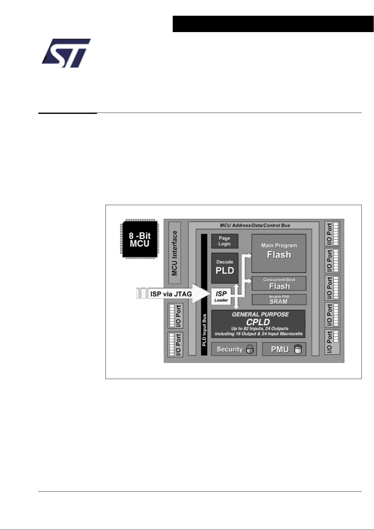
The PSD8XX series of Programmable Microcontroller (MCU) Peripherals brings
In-System-Programmability (ISP) to Flash memory and programmable logic. The result is a
simple and flexible solution for embedded designs. PSD8XX devices combine many of the
peripheral functions found in MCU based applications:
• 4 Mbit of Flash memory
• A secondary Flash memory for boot or data
• Over 3,000 gates of Flash programmable logic
• 64 Kbit SRAM
• Reconfigurable I/O ports
• Programmable power management.
Page 3

PSD8XX Family PSD835G2
2
1.0
Introduction
(Cont.)
Please refer to the revision block at the end of this
document for updated information.
The PSD835G2 device offers two methods to program PSD Flash memory while the PSD
is soldered to a circuit board.
❏ In-System Programming (ISP) via JTAG
An IEEE 1149.1 compliant JTAG-ISP interface is included on the PSD enabling the
entire device (both flash memories, the PLD, and all configuration) to be rapidly
programmed while soldered to the circuit board. This requires no MCU participation,
which means the PSD can be programmed anytime, even while completely blank.
The innovative JTAG interface to flash memories is an industry first, solving key
problems faced by designers and manufacturing houses, such as:
• First time programming – How do I get firmware into the flash the very first time?
JTAG is the answer, program the PSD while blank with no MCU involvement.
• Inventory build-up of pre-programmed devices – How do I maintain an accurate
count of pre-programmed flash memory and PLD devices based on customer
demand? How many and what version? JTAG is the answer, build your hardware
with blank PSDs soldered directly to the board and then custom program just before
they are shipped to customer. No more labels on chips and no more wasted
inventory.
• Expensive sockets – How do I eliminate the need for expensive and unreliable
sockets? JTAG is the answer. Solder the PSD directly to the circuit board. Program
first time and subsequent times with JTAG. No need to handle devices and bend the
fragile leads.
❏ In-Application re-Programming (IAP)
Two independent flash memory arrays are included so the MCU can execute code
from one memory while erasing and programming the other. Robust product firmware
updates in the field are possible over any communication channel (CAN, Ethernet,
UART, J1850, etc) using this unique architecture. Designers are relieved of these
problems:
• Simultaneous read and write to flash memory – How can the MCU program the
same memory from which it is executing code? It cannot. The PSD allows the MCU
to operate the two flash memories concurrently, reading code from one while erasing
and programming the other during IAP.
• Complex memory mapping – How can I map these two memories efficiently?
A Programmable Decode PLD is embedded in the PSD. The concurrent PSD
memories can be mapped anywhere in MCU address space, segment by segment
with extremely high address resolution. As an option, the secondary flash memory
can be swapped out of the system memory map when IAP is complete. A built-in
page register breaks the MCU address limit.
• Separate program and data space – How can I write to flash memory while it
resides in “program” space during field firmware updates, my 80C51 won’t allow it
The flash PSD provides means to “reclassify” flash memory as “data” space during
IAP, then back to “program” space when complete.
PSDsoft – ST’s software development tool – guides you through the design
process step-by-step making it possible to complete an embedded MCU design
capable of ISP/IAP in just hours. Select your MCU and PSDsoft will take you through
the remainder of the design with point and click entry, covering...PSD selection, pin
definitions, programmable logic inputs and outputs, MCU memory map definition, ANSI C
code generation for your MCU, and merging your MCU firmware with the PSD design.
When complete, two different device programmers are supported directly from PSDsoft –
FlashLINK (JTAG) and PSDpro.
The PSD835G2 is available in an 80-pin TQFP package.
Page 4
PSD835G2 PSD8XX Family
❏ A simple interface to 8-bit microcontrollers that use either multiplexed or
non-multiplexed busses. The bus interface logic uses the control signals generated by
the microcontroller automatically when the address is decoded and a read or write is
performed. A partial list of the MCU families supported include:
• Intel 8031, 80196, 80188, 80C251
• Motorola 68HC11 and 68HC16
• Philips 8031 and 80C51XA
• Zilog Z80, Z8 and Z180
• Infineon C500 family
❏ 4 Mbit Flash memory. This is the main Flash memory. It is divided into eight
equal-sized blocks that can be accessed with user-specified addresses.
❏ Internal secondary 256 Kbit Flash boot memory. It is divided into four equal-sized
blocks that can be accessed with user-specified addresses. This secondary memory
brings the ability to execute code and update the main Flash concurrently.
❏ 64 Kbit SRAM. The SRAM’s contents can be protected from a power failure by
connecting an external battery.
❏ CPLD with 16 Output Micro⇔Cells (OMCs) and 24 Input Micro⇔Cells (IMCs). The
CPLD may be used to efficiently implement a variety of logic functions for internal
and external control. Examples include state machines, loadable shift registers, and
loadable counters. The CPLD can also generate eight external chip selects.
❏ Decode PLD (DPLD) that decodes address for selection of internal memory blocks.
❏ 52 individually configurable I/O port pins that can be used for the following functions:
• MCU I/Os
• PLD I/Os
• Latched MCU address output
• Special function I/Os.
• I/O ports may be configured as open-drain outputs.
❏ Standby current as low as 50 µA for 5 V devices.
❏ Built-in JTAG compliant serial port allows full-chip In-System Programmability (ISP).
With it, you can program a blank device or reprogram a device in the factory or the field.
❏ Internal page register that can be used to expand the microcontroller address space
by a factor of 256.
❏ Internal programmable Power Management Unit (PMU) that supports a low power
mode called Power Down Mode. The PMU can automatically detect a lack of
microcontroller activity and put the PSD8XX into Power Down Mode.
❏ Erase/Write cycles:
• Flash memory – 100,000 minimum
• PLD – 1,000 minimum
2.0
Key Features
3
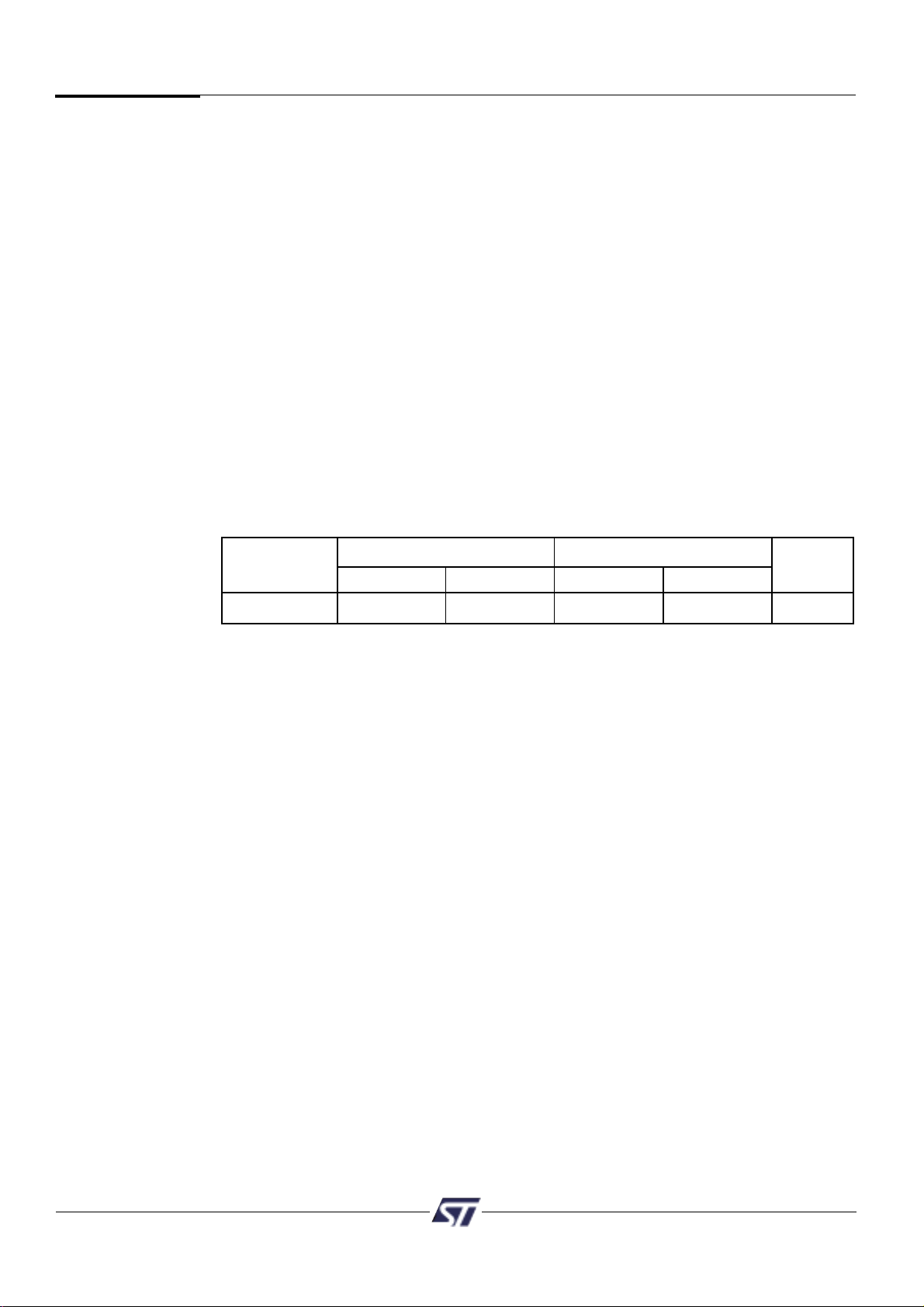
3.0 PSD8XX
Series
Part # Flash
Flash Main Boot
Serial ISP Memory Memory
PSD8XX I/O PLD Input Output PLD JTAG/ISP Kbit Kbit SRAM Supply
Series Device Pins Inputs Macrocells Macrocells Outputs Port 8 Sectors (4 Sectors) Kbit Voltage
PSD835G2 52 24 16 24 Yes 4096 256 64 5V
PSD8XX PSD813F2 27 57 24 16 19 Yes 1024 256 16 5V
PSD834F2 27 57 24 16 19 Yes 2048 256 64 5V
PSD833F2 27 57 24 16 19 Yes 1024 256 64 5V
Table 1. PSD8XX Product Matrix
Page 5
PSD8XX Family PSD835G2
4
PROG.
MCU BUS
INTRF.
ADIO
PORT
CNTL0,
CNTL1,
CNTL2
AD0 – AD15
CLKIN
CLKIN
PORT F
CLKIN
PLD
INPUT
BUS
PROG.
PORT
PORT
A
PROG.
PORT
PORT
B
POWER
MANGMT
UNIT
4 MBIT MAIN FLASH
MEMORY
8 SECTORS
VSTDBY
PA0 – PA7
PROG.
PORT
PORT
F
PROG.
PORT
PORT
G
PROG.
PORT
PORT
E
PB0 – PB7
PROG.
PORT
PORT
C
PROG.
PORT
PORT
D
PF0 – PF7
PG0 – PG7
PE0 – PE7
PC0 – PC7
PD0 – PD3
ADDRESS/DATA/CONTROL BUS
PORT A & B
8 EXT CS to PORT C or F
24 INPUT MICRO⇔CELLS
PORT A ,B & C
82
82
256 KBIT SECONDARY
FLASH MEMORY
(BOOT OR DATA)
4 SECTORS
64 KBIT BATTERY
BACKUP SRAM
RUNTIME CONTROL
AND I/O REGISTERS
SRAM SELECT
PERIP I/O MODE SELECTS
MICRO⇔CELL FEEDBACK OR PORT INPUT
CSIOP
FLASH ISP CPLD
(CPLD)
16 OUTPUT MICRO⇔CELLS
FLASH DECODE
PLD (DPLD
)
PLD, CONFIGURATION
& FLASH MEMORY
LOADER
JTAG
SERIAL
CHANNEL
(
PE6
)
PAGE
REGISTER
EMBEDDED
ALGORITHM
SECTOR
SELECTS
SECTOR
SELECTS
GLOBAL
CONFIG. &
SECURITY
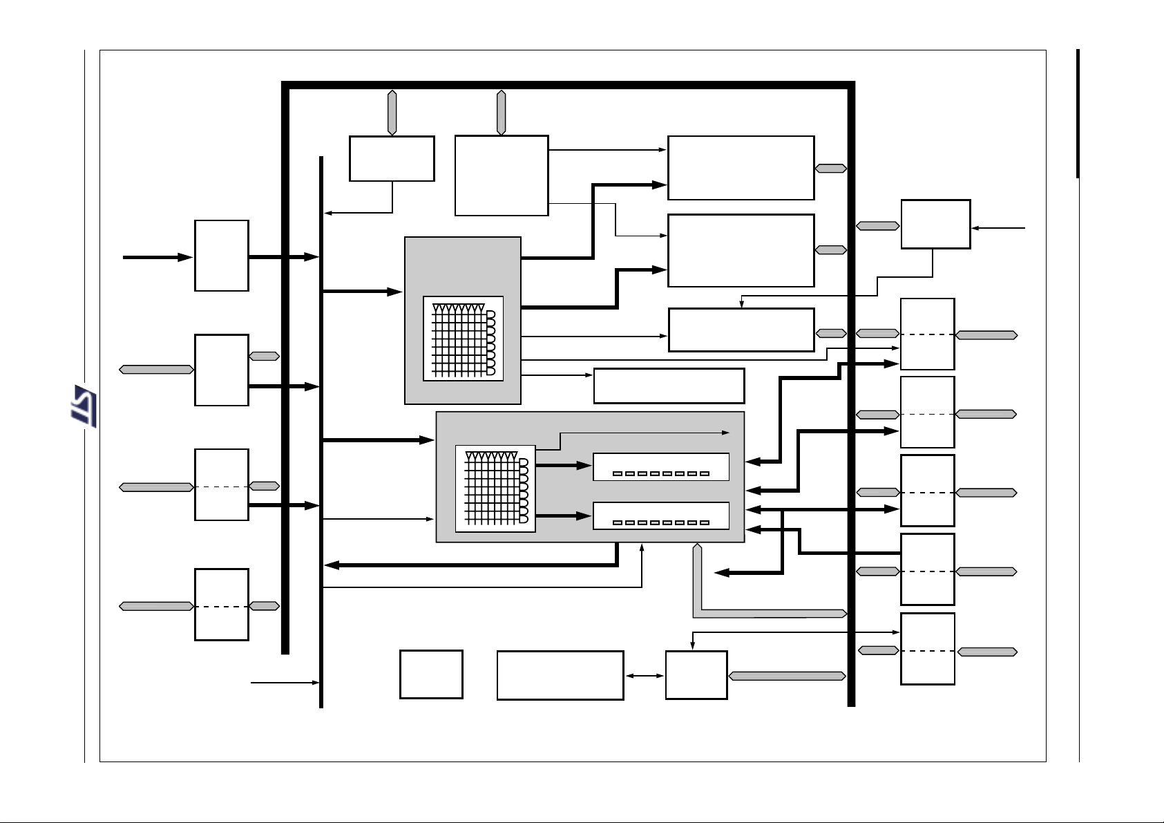
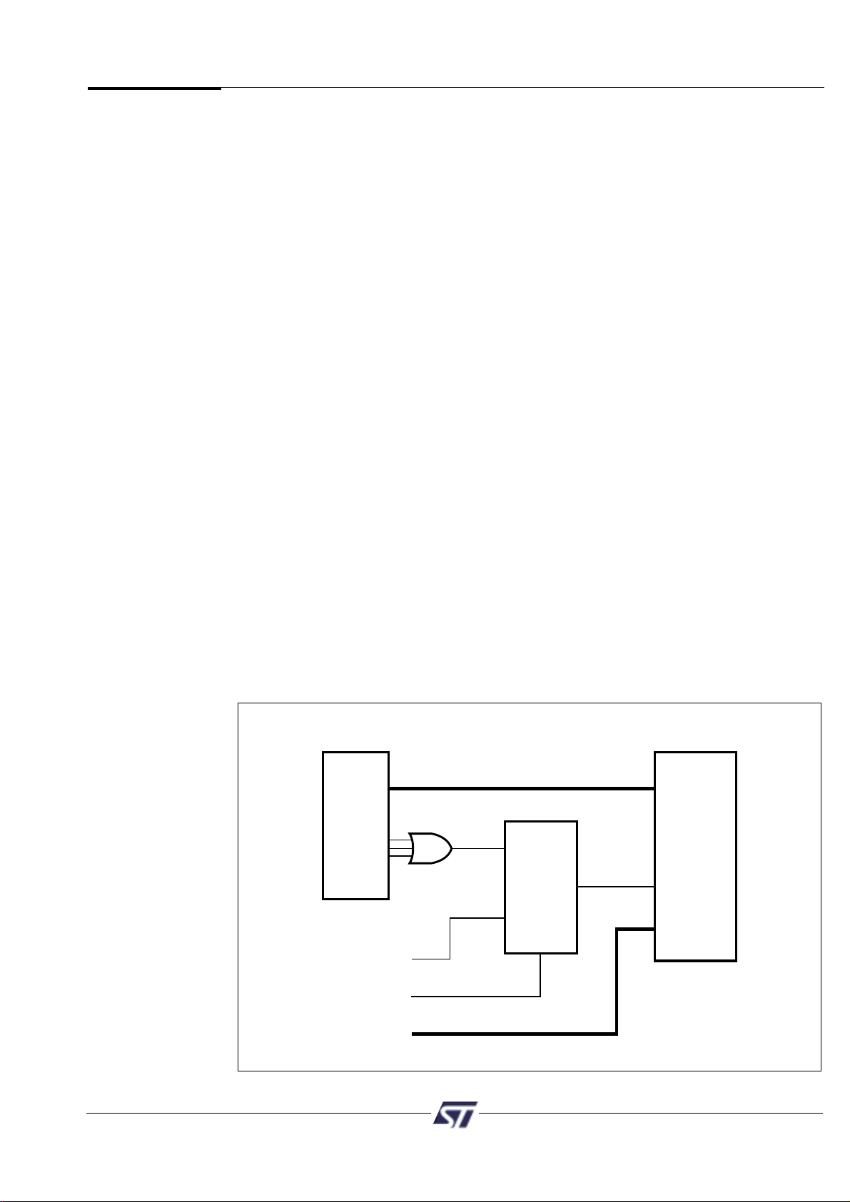
Figure 1. PSD835G2 Block Diagram
*Additional address lines can be brought into PSD via Port A, B, C, D, or F.
Page 6
PSD835G2 PSD8XX Family
5
PSD8XX devices contain several major functional blocks. Figure 1 on page 3 shows the
architecture of the PSD8XX device family. The functions of each block are described
briefly in the following sections. Many of the blocks perform multiple functions and are user
configurable.
4.1 Memory
The PSD835G2 contains the following memories:
• 4 Mbit Flash
• A secondary 256 Kbit Flash memory for boot or data
• 64 Kbit SRAM.
Each of the memories is briefly discussed in the following paragraphs. A more detailed
discussion can be found in section 9.
The 4 Mbit Flash is the main memory of the PSD835G2. It is divided into eight
equally-sized sectors that are individually selectable.
The 256 Kbit secondary Flash memory is divided into four equally-sized sectors. Each
sector is individually selectable.
The 64 Kbit SRAM is intended for use as a scratchpad memory or as an extension to the
microcontroller SRAM. If an external battery is connected to the PSD8XX’s Vstby pin, data
will be retained in the event of a power failure.
Each block of memory can be located in a different address space as defined by the user.
The access times for all memory types includes the address latching and DPLD decoding
time.
4.2 PLDs
The device contains two PLD blocks, each optimized for a different function, as shown in
Table 2. The functional partitioning of the PLDs reduces power consumption, optimizes
cost/performance, and eases design entry.
The Decode PLD (DPLD) is used to decode addresses and generate chip selects for the
PSD835G2 internal memory and registers. The CPLD can implement user-defined logic
functions. The DPLD has combinatorial outputs. The CPLD has 16 Output Micro⇔Cells
and 8 combinatorial outputs. The PSD835G2 also has 24 Input Micro⇔Cells that can be
configured as inputs to the PLDs. The PLDs receive their inputs from the PLD Input Bus
and are differentiated by their output destinations, number of Product Terms, and
Micro⇔Cells.
The PLDs consume minimal power by using Zero-Power design techniques. The speed and
power consumption of the PLD is controlled by the Turbo Bit in the PMMR0 register and
other bits in the PMMR2 registers. These registers are set by the microcontroller at runtime.
There is a slight penalty to PLD propagation time when invoking the non-Turbo bit.
4.3 I/O Ports
The PSD835G2 has 52 I/O pins divided among seven ports (Port A, B, C, D, E, F and G).
Each I/O pin can be individually configured for different functions. Ports can be configured
as standard MCU I/O ports, PLD I/O, or latched address outputs for microcontrollers using
multiplexed address/data busses.
The JTAG pins can be enabled on Port E for In-System Programming (ISP). Ports F and
G can also be configured as a data port for a non-multiplexed bus.
4.4 Microcontroller Bus Interface
The PSD835G2 easily interfaces with most 8-bit microcontrollers that have either
multiplexed or non-multiplexed address/data busses. The device is configured to respond
to the microcontroller’s control signals, which are also used as inputs to the PLDs. Section
9.3.5 contains microcontroller interface examples.
4.0
PSD8XX
Architectural
Overview
Name Abbreviation Inputs Outputs Product Terms
Decode PLD DPLD 82 17 43
Complex PLD CPLD 82 24 150
Table 2. PLD I/O Table
Page 7
PSD8XX
Architectural
Overview
(cont.)
4.5 ISP via JTAG Port
In-System Programming can be performed through the JTAG pins on Port E. This serial
interface allows complete programming of the entire PSD835G2 device. A blank device
can be completely programmed. The JTAG signals (TMS, TCK, TSTAT, TERR, TDI, TDO)
can be multiplexed with other functions on Port E. Table 3 indicates the JTAG signals pin
assignments.
4.6 In-System Programming (ISP)
Using the JTAG signals on Port E, the entire PSD835G2 (memory, logic, configuration)
device can be programmed or erased without the use of the microcontroller.
Port E Pins JTAG Signal
PE0 TMS
PE1 TCK
PE2 TDI
PE3 TDO
PE4 TSTAT
PE5 TERR
Table 3. JTAG Signals on Port E
PSD8XX Family PSD835G2
6
4.7 In-Application re-Programming (IAP)
The main Flash memory can also be programmed in-system by the microcontroller
executing the programming algorithms out of the secondary Flash memory, or SRAM.
Since this is a sizable separate block, the application can also continue to operate. The
secondary Flash boot memory can be programmed the same way by executing out of the
main Flash memory. Table 4 indicates which programming methods can program different
functional blocks of the PSD8XX.
Device
Functional Block JTAG-ISP Programmer IAP
Main Flash memory Yes Yes Yes
Flash Boot memory Yes Yes Yes
PLD Array (DPLD and CPLD) Yes Yes No
PSD Configuration Yes Yes No
Table 4. Methods of Programming Different Functional Blocks of the PSD835G2
4.8 Page Register
The eight-bit Page Register expands the address range of the microcontroller by up to
256 times.The paged address can be used as part of the address space to access
external memory and peripherals or internal memory and I/O. The Page Register can also
be used to change the address mapping of blocks of Flash memory into different memory
spaces for IAP.
4.9 Power Management Unit
The Power Management Unit (PMU) in the PSD835G2 gives the user control of the
power consumption on selected functional blocks based on system requirements. The
PMU includes an Automatic Power Down unit (APD) that will turn off device functions due
to microcontroller inactivity. The APD unit has a Power Down Mode that helps reduce
power consumption.
The PSD835G2 also has some bits that are configured at run-time by the MCU to reduce
power consumption of the CPLD. The turbo bit in the PMMR0 register can be turned off
and the CPLD will latch its outputs and go to standby until the next transition on its inputs.
Additionally, bits in the PMMR2 register can be set by the MCU to block signals from
entering the CPLD to reduce power consumption. See section 9.5.
Page 8
PSD835G2 PSD8XX Family
7
Define General Purpose
Logic in CPLD
Merge MCU Firmware
with PSD Configuration
ST
PSD Programmer
*.OBJ FILE
Point and click definition of
combinatorial and registered logic
in CPLD. Access to HDL is
available if needed.
Define PSD Pin and
Node functions
Point and click definition of
PSD pin functions, internal nodes,
and MCU system memory map.
Choose MCU and PSD
Automatically Configures MCU
bus interface and other PSD
attributes.
PSDPro or
FlashLink (JTAG)
A composite object file is created
containing MCU firmware and
PSD configuration.
C Code Generation
Generate C Code
Specific to PSD
Finctions
User's choice of
Microcontroller
Compiler/Linker
*.OBJ file
available
for 3rd party
programmers
(Conventional or JTAG-ISP)
MCU Firmware
Hex or S-Record
format
Figure 2. PSDsoft Development Tool
5.0
Development
System
The PSD8XX series is supported by PSDsoft a Windows-based (95, 98, NT) software
development tool. A PSD design is quickly and easily produced in a point and click
environment. The designer does not need to enter Hardware Definition Language (HDL)
equations (unless desired) to define PSD pin functions and memory map information. The
general design flow is shown in Figure 2 below. PSDsoft is available from our web site
(www.st.com/psm) or other distribution channels.
PSDsoft directly supports two low cost device programmers from ST. PSDpro
and FlashLINK (JTAG). Both of these programmers may be purchased through your local
rep/distributor, or directly from our web site using a credit card. The PSD8XX is also
supported by third party device programmers, see web site for current list.
Page 9
PSD8XX Family PSD835G2
8
The following table describes the pin names and pin functions of the PSD835G2. Pins that
have multiple names and/or functions are defined using PSDsoft.
6.0
Table 5.
PSD835G2
Pin
Descriptions
Pin*
(TQFP
Pin Name Pkg.) Type Description
ADIO0-7 3-7 I/O This is the lower Address/Data port. Connect your MCU
10-12 address or address/data bus according to the following rules:
1. If your MCU has a multiplexed address/data bus where the
data is multiplexed with the lower address bits, connect
AD[0:7] to this port.
2. If your MCU does not have a multiplexed address/data bus,
connect A[0:7] to this port.
3. If you are using an 80C51XA in burst mode, connect
A4/D0 through A11/D7 to this port.
ALE or AS latches the address. The PSD drives data out only
if the read signal is active and one of the PSD functional blocks
was selected. The addresses on this port are passed to the
PLDs.
ADIO8-15 13-20 I/O This is the upper Address/Data port. Connect your MCU
address or address/data bus according to the following rules:
1. If your MCU has a multiplexed address/data bus where the
data is multiplexed with the lower address bits, connect
A[8:15 ] to this port.
2. If your MCU does not have a multiplexed address/data bus,
connect A[8:15 ] to this port.
3. If you are using an 80C251 in page mode, connect AD[8:15]
to this port
4. If you are using an 80C51XA in burst mode, connect
A[12:19] to this port.
ALE or AS latches the address. The PSD drives data out only
if the read signal is active and one of the PSD functional
blocks was selected. The addresses on this port are passed
to the PLDs.
CNTL0 59 I The following control signals can be connected to this port,
based on your MCU:
1. WR — active-low write input.
2. R_W — active-high read/active low write input.
This pin is connected to the PLDs. Therefore, these signals can
be used in decode and other logic equations.
CNTL1 60 I The following control signals can be connected to this port,
based on your MCU:
1. RD — active-low read input.
2. E — E clock input.
3. DS — active-low data strobe input.
4. PSEN — connect PSEN to this port when it is being used as
an active-low read signal. For example, when the 80C251
outputs more than 16 address bits, PSEN is actually the read
signal.
This pin is connected to the PLDs. Therefore, these signals can
be used in decode and other logic equations.
CNTL2 40 I This pin can be used to input the PSEN (Program Select
Enable) signal from any MCU that uses this signal for code
exclusively. If your MCU does not output a Program Select
Enable signal, this port can be used as a generic input. This
port is connected to the PLD as input.
Reset 39 I Active low input. Resets I/O Ports, PLD Micro⇔Cells, some of
the configuration registers and JTAG registers. Must be active
at power up. Reset also aborts the Flash programming/erase
cycle that is in progress.
Page 10
PSD835G2 PSD8XX Family
Pin*
(TQFP
Pin Name Pkg.) Type Description
PA0-PA7 51-58 I/O Port A, PA0-7. This port is pin configurable and has multiple
CMOS functions:
or Open 1. MCU I/O — standard output or input port
Drain 2. CPLD Micro⇔Cell (MCell A0-7) output.
3. Latched, transparent or registered PLD input.
PB0-PB7 61-68 I/O Port B, PB0-7. This port is pin configurable and has multiple
CMOS functions:
or Open 1. MCU I/O — standard output or input port.
Drain 2. CPLD Micro⇔Cell (MCell B0-7) output.
3. Latched, transparent or registered PLD input.
PC0-PC7 41-48 I/O Port C, PC0-7. This port is pin configurable and has multiple
CMOS functions:
or Slew 1. MCU I/O — standard output or input port.
Rate 2. External chip select (ECS0-7) output.
3. Latched, transparent or registered PLD input.
PD0 79 I/O Port D pin PD0 can be configured as:
CMOS 1. ALE or AS input — latches addresses on ADIO0-15 pins
or Open 2. AS input — latches addresses on ADIO0-15 pins on the
Drain rising edge.
3. Input to the PLD.
4. Transparent PLD input.
PD1 80 I/O Port D pin PD1 can be configured as:
CMOS 1. MCU I/O
or Open 2. Input to the PLD.
Drain 3. CLKIN clock input — clock input to the CPLD
Micro⇔Cells, the APD power down counter and CPLD
AND Array.
PD2 1 I/O Port D pin PD2 can be configured as:
CMOS 1. MCU I/O
or Open 2. Input to the PLD.
Drain 3. CSI input — chip select input. When low, the CSI enables
the internal PSD memories and I/O. When high, the
internal memories are disabled to conserve power. CSI
trailing edge can get the part out of power-down mode.
PD3 2 I/O
Port D pin PD3 can be configured as:
CMOS
1. MCU I/O
or Open
2. Input to the PLD.
Drain
PE0 71 I/O Port E, PE0. This port is pin configurable and has multiple
CMOS functions:
or Open 1. MCU I/O — standard output or input port.
Drain 2. Latched address output.
3. TMS input for JTAG/ISP interface.
PE1 72 I/O Port E, PE1. This port is pin configurable and has multiple
CMOS functions:
or Open 1. MCU I/O — standard output or input port.
Drain 2. Latched address output.
3. TCK input for JTAG/ISP interface (Schmidt Trigger).
PE2 73 I/O Port E, PE2. This port is pin configurable and has multiple
CMOS functions:
or Open 1. MCU I/O — standard output or input port.
Drain 2. Latched address output.
3. TDI input for JTAG/ISP interface.
Table 5.
PSD835G2
Pin
Descriptions
(cont.)
9
Page 11
PSD8XX Family PSD835G2
10
Pin*
(TQFP
Pin Name Pkg.) Type Description
PE3 74 I/O Port E, PE3. This port is pin configurable and has multiple
CMOS functions:
or Open 1. MCU I/O — standard output or input port.
Drain 2. Latched address output.
3. TDO output for JTAG/ISP interface.
PE4 75 I/O Port E, PE4. This port is pin configurable and has multiple
CMOS functions:
or Open 1. MCU I/O — standard output or input port.
Drain 2. Latched address output.
3. TSTAT output for the ISP interface.
4. Rdy/Bsy — for in-circuit Parallel Programming.
PE5 76 I/O Port E, PE5. This port is pin configurable and has multiple
CMOS functions:
or Open 1. MCU I/O — standard output or input port.
Drain 2. Latched address output.
3. TERR active low output for ISP interface.
PE6 77 I/O Port E, PE6. This port is pin configurable and has multiple
CMOS functions:
or Open 1. MCU I/O — standard output or input port.
Drain 2. Latched address output.
3. Vstby — SRAM standby voltage input for battery
backup SRAM
PE7 78 I/O Port E, PE7. This port is pin configurable and has multiple
CMOS functions:
or Open 1. MCU I/O — standard output or input port.
Drain 2. Latched address output.
3. Vbaton — battery backup indicator output. Goes high when
power is drawn from an external battery.
PF0-PF7 31-38 I/O Port F, PF0-7. This port is pin configurable and has multiple
CMOS functions:
or Open 1. MCU I/O — standard output or input port.
Drain 2. Input to the PLD.
3. Latched address outputs.
4. As address A0-3 inputs in 80C51XA mode
5. As data bus port (D0-7) in non-multiplexed bus configuration
PG0-PG7 21-28 I/O Port G, PG0-7. This port is pin configurable and has multiple
CMOS functions:
or Open 1. MCU I/O — standard output or input port.
Drain 2. Latched address outputs.
GND 8,30,
49,50,
70
V
CC
9,29,
69
Table 5.
PSD835G2
Pin
Descriptions
(cont.)
Page 12
PSD835G2 PSD8XX Family
11
Table 6 shows the offset addresses to the PSD835G2 registers relative to the CSIOP base
address. The CSIOP space is the 256 bytes of address that is allocated by the user to the
internal PSD835G2 registers. Table 6 provides brief descriptions of the registers in CSIOP
space. For a more detailed description, refer to section 9.
7.0 PSD835G2
Register
Description and
Address Offset
Register Name Port A Port B Port C Port D Port E Port F Port G Other* Description
Data In 00 01 10 11 30 40 41
Reads Port pin as input,
MCU I/O input mode
Control 32 42 43
Selects mode between
MCU I/O or Address Out
Stores data for output
Data Out 04 05 14 15 34 44 45 to Port pins, MCU I/O
output mode
Direction 06 07 16 17 36 46 47
Configures Port pin as
input or output
Configures Port pins as
either CMOS or Open
Drive Select 08 09 18 19 38 48 49 Drain on some pins, while
selecting high slew rate
on other pins.
Input Micro⇔Cell 0A 0B 1A Reads Input Micro⇔Cells
Reads the status of the
Enable Out 0C 0D 1C 4C output enable to the I/O
Port driver
Read – reads output of
Output Micro⇔Cells A
Micro⇔Cells A
20
Write – loads Micro⇔cell
Flip-Flops
Read – reads output of
Output Micro⇔Cells B
Micro⇔Cells B
21
Write – loads Micro⇔cell
Flip-Flops
Mask
22
Blocks writing to the
Micro⇔Cells A Output Micro⇔Cells A
Mask
23
Blocks writing to the
Micro⇔Cells B Output Micro⇔Cells B
Flash Protection
C0 Read only – Flash Sector
Protection
Flash Boot
Read only – PSD Security
Protection
C2 and Flash Boot Sector
Protection
JTAG Enable C7 Enables JTAG Port
PMMR0 B0
Power Management
Register 0
PMMR2 B4
Power Management
Register 2
Page E0 Page Register
Places PSD memory
VM E2
areas in Program and/or
Data space on an
individual basis.
Memory_ID0 F0
Read only – Flash and
SRAM size
Memory_ID1 F1
Read only – Boot type
and size
Table 6. Register Address Offset
Page 13
PSD8XX Family PSD835G2
12
Bit 7 Bit 6 Bit 5 Bit 4 Bit 3 Bit 2 Bit 1 Bit 0
Port Pin 7 Port Pin 6 Port Pin 5 Port Pin 4 Port Pin 3 Port Pin 2 Port Pin 1 Port Pin 0
Data In Registers – Port A, B, C, D, E, F and G
8.0
Register Bit
Definition
All the registers in the PSD835G2 are included here for reference. Detail description of the
registers are found in the Functional Block section of the Data Sheet.
Bit definitions:
Read only registers, read Port pin status when Port is in MCU I/O input Mode.
Bit 7 Bit 6 Bit 5 Bit 4 Bit 3 Bit 2 Bit 1 Bit 0
Port Pin 7 Port Pin 6 Port Pin 5 Port Pin 4 Port Pin 3 Port Pin 2 Port Pin 1 Port Pin 0
Data Out Registers – Port A, B, C, D, E, F and G
Bit definitions:
Latched data for output to Port pin when pin is configured in MCU I/O output mode.
Bit 7 Bit 6 Bit 5 Bit 4 Bit 3 Bit 2 Bit 1 Bit 0
Port Pin 7 Port Pin 6 Port Pin 5 Port Pin 4 Port Pin 3 Port Pin 2 Port Pin 1 Port Pin 0
Direction Registers – Port A, B, C, D, E, F and G
Bit definitions:
Set Register Bit to 0 = configure corresponding Port pin in Input mode (default).
Set Register Bit to 1 = configure corresponding Port pin in Output mode.
Bit 7 Bit 6 Bit 5 Bit 4 Bit 3 Bit 2 Bit 1 Bit 0
Port Pin 7 Port Pin 6 Port Pin 5 Port Pin 4 Port Pin 3 Port Pin 2 Port Pin 1 Port Pin 0
Control Registers – Ports E, F and G
Bit definitions:
Set Register Bit to 0 = configure corresponding Port pin in MCU I/O mode (default).
Set Register Bit to 1 = configure corresponding Port pin in Latched Address Out mode.
Bit 7 Bit 6 Bit 5 Bit 4 Bit 3 Bit 2 Bit 1 Bit 0
Port Pin 7 Port Pin 6 Port Pin 5 Port Pin 4 Port Pin 3 Port Pin 2 Port Pin 1 Port Pin 0
Drive Registers – Ports A, B, D, E, and G
Bit definitions:
Set Register Bit to 0 = configure corresponding Port pin in CMOS output driver (default).
Set Register Bit to 1 = configure corresponding Port pin in Open Drain output driver.
Bit 7 Bit 6 Bit 5 Bit 4 Bit 3 Bit 2 Bit 1 Bit 0
Port Pin 7 Port Pin 6 Port Pin 5 Port Pin 4 Port Pin 3 Port Pin 2 Port Pin 1 Port Pin 0
Drive Registers – Ports C and F
Bit definitions:
Set Register Bit to 0 = configure corresponding Port pin as CMOS output driver (default).
Set Register Bit to 1 = configure corresponding Port pin in Slew Rate mode.
Bit 7 Bit 6 Bit 5 Bit 4 Bit 3 Bit 2 Bit 1 Bit 0
Port Pin 7 Port Pin 6 Port Pin 5 Port Pin 4 Port Pin 3 Port Pin 2 Port Pin 1 Port Pin 0
Enable Out Registers – Ports A, B, C and F
Bit definitions: Read Only Registers
Register Bit <j> = 0 indicates Port pin driver is in tri-state mode (default).
Register Bit <j> = 1 indicates Port pin driver is enabled.
Page 14
PSD835G2 PSD8XX Family
13
8.0
Register Bit
Definition
(cont.)
Bit 7 Bit 6 Bit 5 Bit 4 Bit 3 Bit 2 Bit 1 Bit 0
IMcell7 IMcell6 IMcell5 IMcell4 IMcell3 IMcell2 IMcell1 IMcell0
Input Micro⇔Cells – Ports A, B and C
Bit definitions: Read Only Registers
Read Input Micro⇔Cell[7:0] status on Ports A, B and C.
Bit 7 Bit 6 Bit 5 Bit 4 Bit 3 Bit 2 Bit 1 Bit 0
Mcella7 Mcella6 Mcella5 Mcella4 Mcella3 Mcella2 Mcella1 Mcella0
Output Micro⇔Cells A Register
Bit definitions:
Write Register: Load Micro⇔CellA[7:0] with 0 or 1.
Read Register: Read Micro⇔CellA[7:0] output status.
Bit 7 Bit 6 Bit 5 Bit 4 Bit 3 Bit 2 Bit 1 Bit 0
Mcellb7 Mcellb6 Mcellb5 Mcellb4 Mcellb3 Mcellb2 Mcellb1 Mcellb0
Output Micro⇔Cells B Register
Bit definitions:
Write Register: Load Micro⇔CellB[7:0] with 0 or 1.
Read Register: Read Micro⇔CellB[7:0] output status.
Bit 7 Bit 6 Bit 5 Bit 4 Bit 3 Bit 2 Bit 1 Bit 0
Mcella7 Mcella6 Mcella5 Mcella4 Mcella3 Mcella2 Mcella1 Mcella0
Mask Micro⇔Cells A Register
Bit definitions:
Register Bit <j> to 0 = allow Micro⇔CellA<j> flip flop to be loaded by MCU (default).
Register Bit <j> to 1 = does not allow Micro⇔CellA<j> flip flop to be loaded by MCU.
Bit 7 Bit 6 Bit 5 Bit 4 Bit 3 Bit 2 Bit 1 Bit 0
Mcellb7 Mcellb6 Mcellb5 Mcellb4 Mcellb3 Mcellb2 Mcellb1 Mcellb0
Mask Micro⇔Cells B Register
Bit definitions:
Register Bit <j> to 0 = allow Micro⇔CellB<j> flip flop to be loaded by MCU (default).
Register Bit <j> to 1 = does not allow Micro⇔CellB<j> flip flop to be loaded by MCU.
Bit 7 Bit 6 Bit 5 Bit 4 Bit 3 Bit 2 Bit 1 Bit 0
Sec7_Prot Sec6_Prot Sec5_Prot Sec4_Prot Sec3_Prot Sec2_Prot Sec1_Prot Sec0_Prot
Flash Protection Register
Bit definitions: Read Only Register
Sec<i>_Prot 1 = Flash Sector <i> is write protected.
Sec<i>_Prot 0 = Flash Sector <i> is not write protected.
Bit 7 Bit 6 Bit 5 Bit 4 Bit 3 Bit 2 Bit 1 Bit 0
Security_Bit
***
Sec3_Prot Sec2_Prot Sec1_Prot Sec0_Prot
Flash Boot Protection Register
Bit definitions:
Sec<i>_Prot 1 = Boot Block Sector <i> is write protected.
Sec<i>_Prot 0 = Boot Block Sector <i> is not write protected.
Security_Bit 0 = Security Bit in device has not been set.
1 = Security Bit in device has been set.
Page 15
PSD8XX Family PSD835G2
14
Bit 7 Bit 6 Bit 5 Bit 4 Bit 3 Bit 2 Bit 1 Bit 0
*******
JTAG_Enable
JTAG Enable Register
Bit definitions:
JTAG_Enable 1 = JTAG Port is Enabled.
0 = JTAG Port is Disabled.
8.0
Register Bit
Definition
(cont.)
Bit 7 Bit 6 Bit 5 Bit 4 Bit 3 Bit 2 Bit 1 Bit 0
Pgr7 Pgr6 Pgr5 Pgr4 Pgr3 Pgr2 Pgr1 Pgr0
Page Register
Bit definitions:
Configure Page input to PLD. Default Pgr[7:0] = 00.
Bit 7 Bit 6 Bit 5 Bit 4 Bit 3 Bit 2 Bit 1 Bit 0
**
PLD PLD PLD
*
APD
*
Mcells clk array-clk Turbo enable
PMMR0 Register
Bit definitions: (default is 0)
Bit 1 0 = Automatic Power Down (APD) is disabled.
1 = Automatic Power Down (APD) is enabled.
Bit 3 0 = PLD Turbo is on.
1 = PLD Turbo is off, saving power.
Bit 4 0 = CLKIN input to the PLD AND array is connected.
Every CLKIN change will power up the ZPLD when Turbo bit is off.
1 = CLKIN input to PLD AND array is disconnected, saving power.
Bit 5 0 = CLKIN input to the PLD Micro ⇔Cells is connected.
1 = CLKIN input to the PLD Micro ⇔Cells is disconnected, saving power.
*Not used bit should be set to zero.
Bit 7 Bit 6 Bit 5 Bit 4 Bit 3 Bit 2 Bit 1 Bit 0
*
PLD PLD PLD PLD PLD
**
array WRh array Ale array Cntl2 array Cntl1 array Cntl0
PMMR1 Register
Bit definitions (default is 0):
Bit 0 0 = Address A[7:0] are connected into the PLD array.
1 = Address A[7:0] are blocked from the PLD array, saving power.
Note: in XA mode, A3-0 come from PF3-0 and A7-4 come from ADIO7-4.
Bit 2 0 = Cntl0 input to the PLD AND array is connected.
1 = Cntl0 input to the PLD AND array is disconnected, saving power.
Bit 3 0 = Cntl1 input to the PLD AND array is connected.
1 = Cntl1 input to the PLD AND array is disconnected, saving power.
Bit 4 0 = Cntl2 input to the PLD AND array is connected.
1 = Cntl2 input to the PLD AND array is disconnected, saving power.
Bit 5 0 = Ale input to the PLD AND array is connected.
1 = Ale input to the PLD AND array is disconnected, saving power.
Bit 6 0 = WRh/DBE input to the PLD AND array is connected.
1 = WRh/DBE input to the PLD AND array is disconnected, saving power.
*Not used bit should be set to zero.
Page 16
PSD835G2 PSD8XX Family
15
Bit 7 Bit 6 Bit 5 Bit 4 Bit 3 Bit 2 Bit 1 Bit 0
Periph-
**
FL_data Boot_data FL_code Boot_code SR_code
mode
VM Register
Bit definitions:
Bit 0 0 = PSEN can’t access SRAM in 80C51XA modes.
1 = PSEN can access SRAM in 80C51XA modes.
Bit 1 0 = PSEN can’t access Boot in 80C51XA modes.
1 = PSEN can access Boot in 80C51XA modes.
Bit 2 0 = PSEN can’t access main Flash in 80C51XA modes.
1 = PSEN can access main Flash in 80C51XA modes.
Bit 3 0 = RD can’t access Boot in 80C51XA modes.
1 = RD can access Boot in 80C51XA modes.
Bit 4 0 = RD can’t access main Flash in 80C51XA modes.
1 = RD can access main Flash in 80C51XA modes.
Bit 7 0 = Peripheral mode of Port F is disabled.
1 = Peripheral mode of Port F is enabled.
Note: Upon reset, Bit1-Bit4 are loaded to configurations selected by the user in PSDsoft. Bit 0 and Bit 7 are
always cleared by reset. Bit 0 to Bit 4 are active only when the device is configured in Philips 80C51XA
mode.
* Not used bit should be set to zero
8.0
Register Bit
Definition
(cont.)
Bit 7 Bit 6 Bit 5 Bit 4 Bit 3 Bit 2 Bit 1 Bit 0
S_size 3 S_size 2 S_size 1 S_size 0 F_size 3 F_size 2 F_size 1 F_size 0
Memory_ID0 Register
Bit definitions:
F_size[3:0] = 4h, main Flash size is 2M bit.
F_size[3:0] = 5h, main Flash size is 8M bit.
S_size[3:0] = 0h, SRAM size is 0K bit.
S_size[3:0] = 1h, SRAM size is 16K bit.
S_size[3:0] = 3h, SRAM size is 64K bit.
Bit 7 Bit 6 Bit 5 Bit 4 Bit 3 Bit 2 Bit 1 Bit 0
**
B_type 1 B_type 0 B_size 3 B_size 2 B_size 1 B_size 0
Memory_ID1 Register
Bit definitions:
B_size[3:0] = 0h, Boot block size is 0K bit.
B_size[3:0] = 2h, Boot block size is 256K bit.
B_type[1:0] = 0h, Boot block is Flash memory.
*Not used bit should be set to zero.
Page 17
PSD8XX Family PSD835G2
16
9.0
The
PSD835G2
Functional
Blocks
As shown in Figure 1, the PSD835G2 consists of six major types of functional blocks:
❏ Memory Blocks
❏ PLD Blocks
❏ Bus Interface
❏ I/O Ports
❏ Power Management Unit
❏ JTAG-ISP Interface
The functions of each block are described in the following sections. Many of the blocks
perform multiple functions, and are user configurable.
9.1 Memory Blocks
The PSD835G2 has the following memory blocks:
• The main Flash memory
• Secondary Flash memory
• SRAM.
The memory select signals for these blocks originate from the Decode PLD (DPLD) and
are user-defined in PSDsoft.
Table 7 summarizes which versions of the PSD835G2 contain which memory blocks.
Main Flash Secondary Flash
Device Flash Size Sector Size Block Size Sector Size SRAM
PSD835G2 512KB 64KB 32KB 8KB 8KB
Table 7. Memory Blocks
9.1.1 Main Flash and Secondary Flash Memory Description
The main Flash memory block is divided evenly into eight sectors. The secondary Flash
memory is divided into four sectors of eight Kbytes each. Each sector of either memory
can be separately protected from program and erase operations.
Flash memory may be erased on a sector-by-sector basis and programmed word-by-word.
Flash sector erasure may be suspended while data is read from other sectors of memory
and then resumed after reading.
During a program or erase of Flash, the status can be output on the Rdy/Bsy pin of Port
PE4. This pin is set up using PSDsoft.
9.1.1.1 Memory Block Selects
The decode PLD in the PSD835G2 generates the chip selects for all the internal memory
blocks (refer to the PLD section). Each of the eight Flash memory sectors have a
Flash Select signal (FS0 -FS7) which can contain up to three product terms. Each of the
four Secondary Flash memory sectors have a Select signal (CSBOOT0-3) which can
contain up to three product terms. Having three product terms for each sector select signal
allows a given sector to be mapped in different areas of system memory. When using a
microcontroller (80C51) with separate Program and Data space, these flexible select
signals allow dynamic re-mapping of sectors from one space to the other before and after
IAP.
Page 18
PSD835G2 PSD8XX Family
17
9.1.1.2 Upper and Lower Block IN MAIN FLASH SECTOR
The PSD835G2’s main Flash has eight 64K bytes sector. The 64K byte sector size may
cause some difficulty in code mapping for an 8-bit MCU with only 64K byte address space.
To resolve this mapping issue, the PSD835G2 provides additional logic (Figure 3) for the
user to split the 8 sectors such that each sector has a lower and upper 32K byte block, and
the two blocks can reside in different pages but in the same address range.
If your design works with 64KB sectors, you don’t need to configure this logic. If the design
requires 32KB blocks in each sector, you need to define a “FA15” PLD equation in
PSDsoft as the A15 address input to the main Flash module. FA15 consists of 3 product
terms and will control whether the MCU is accessing the lower or upper 32KB in the
selected sector. Below is an example for Flash sector chip select FS0. A typical equation
is FA15 = pgr4 of the Page Register. When pgr4 is 0 (page 00), the lower 32KB is
selected. When pgr4 is switched to 1 by the user, the upper 32KB is selected. PSDsoft will
automatically generate the PLD equations shown, based on your point and click
selections.
page = [pgr7...pgr0]; “Page Register output
“Sector Chip Select Equation
FS0 = ((0000h <= address <= 7FFFh) & page = 00h) # “select first 32KB block
((0000h <= address <= 7FFFh) & page = 10h); “select second 32KB block
FA15 = pgr4; “as address A15 input to the main Flash
If no FA15 equation is defined in PSDsoft, the A15 that comes from the MCU address bus
will be routed as input to the main Flash instead of FA15. The FA15 equation has no
impact in the Sector Erase operation. Note: FA15 affects all eight sectors of the main Flash
simultaneously, you cannot direct FA15 to a particular Flash sector only.
9.1.1.3 The Ready/Busy Pin (PE4)
Pin PE4 can be used to output the Ready/Busy status of the PSD835G2. The output on
the pin will be a ‘0’ (Busy) when Flash memory blocks are being written to, or when the
Flash memory block is being erased. The output will be a ‘1’ (Ready) when no write or
erase operation is in progress.
The
PSD835G2
Functional
Blocks
(cont.)
DPLD
ARRAY
FA15
A15
* Set by PSDsoft
FLASH CHIP SELECTS FS0-7
MUX
NVM CONTROL BIT
*
MAIN
FLASH
SECTOR
ADDR A15
A [14:0]
Figure 3. Selecting the Upper or Lower Block in a Main Flash Sector
Page 19

9.1.1.4 Memory Operation
The main Flash and secondary Flash memories are addressed through the microcontroller
interface on the PSD835G2 device. The microcontroller can access these memories in one
of two ways:
❏ The microcontroller can execute a typical bus write or read operation just as it would
if accessing a RAM or ROM device using standard bus cycles.
❏ The microcontroller can execute a specific instruction that consists of several write
and read operations. This involves writing specific data patterns to special addresses
within the Flash to invoke an embedded algorithm. These instructions are summarized
in Table 8.
Typically, Flash memory can be read by the microcontroller using read operations, just
as it would read a ROM device. However, Flash memory can only be erased and
programmed with specific instructions. For example, the microcontroller cannot write a
single byte directly to Flash memory as one would write a byte to RAM. To program a byte
into Flash memory, the microcontroller must execute a program instruction sequence, then
test the status of the programming event. This status test is achieved by a read
operation or polling the Rdy/Busy pin (PE4).
The Flash memory can also be read by using special instructions to retrieve particular
Flash device information (sector protect status and ID).
9.1.1.4.1 Instructions
An instruction is defined as a sequence of specific operations. Each received byte is
sequentially decoded by the PSD and not executed as a standard write operation. The
instruction is executed when the correct number of bytes are properly received and the
time between two consecutive bytes is shorter than the time-out value. Some instructions
are structured to include read operations after the initial write operations.
The sequencing of any instruction must be followed exactly. Any invalid combination of
instruction bytes or time-out between two consecutive bytes while addressing Flash
memory will reset the device logic into a read array mode (Flash memory reads like a
ROM device).
The PSD835G2 main Flash and secondary Flash support these instructions (see Table 8):
❏ Erase memory by chip or sector
❏ Suspend or resume sector erase
❏ Program a byte
❏ Reset to read array mode
❏ Read Main Flash Identifier value
❏ Read sector protection status
❏ Bypass Instruction
These instructions are detailed in Table 8. For efficient decoding of the instructions, the
first two bytes of an instruction are the coded cycles and are followed by a command byte
or confirmation byte. The coded cycles consist of writing the data AAh to address X555h
during the first cycle and data 55h to address XAAAh during the second cycle (unless the
Bypass Instruction feature is used. See 9.1.1.7). Address lines A15-A12 are don’t care
during the instruction write cycles. However, the appropriate sector select signal (FSi or
CSBOOTi) must be selected.
The main Flash and the secondary Flash Block have the same set of instructions (except
Read main Flash ID). The chip selects of the Flash memory will determine which Flash will
receive and execute the instruction. The main Flash is selected if any one of the FS0-7 is
active, and the secondary Flash Block is selected if any one of the CSBOOT0-3 is active.
The
PSD835G2
Functional
Blocks
(cont.)
PSD8XX Family PSD835G2
18
Page 20
PSD835G2 PSD8XX Family
19
The
PSD835G2
Functional
Blocks
(cont.)
FS0-7
or
Instruction CSBOOT0-3 Cycle 1 Cycle 2 Cycle 3 Cycle 4 Cycle5 Cycle 6 Cycle 7
Read (Note 5) 1 “Read”
RA RD
Read Main Flash ID 1 AAh 55h 90h “Read”
(Notes 6,13) @555h @AAAh @555h ID
@x01h
Read Sector Protection 1 AAh 55h 90h “Read”
(Notes 6,8,13) @555h @AAAh @555h 00h or 01h
@x02h
Program a Flash Byte 1 AAh 55h A0h PD@PA
@555h @AAAh @555h
Erase One Flash Sector 1 AAh 55h 80h AAh 55h 30h 30h
@555h @AAAh @555h @555h @AAAh @SA @next SA
(Note 7)
Erase Flash Block 1 AAh 55h 80h AAh 55h 10h
(Bulk Erase) @555h @AAAh @555h @555h @AAAh @555h
Suspend Sector Erase 1 B0h
(Note 11) @xxxh
Resume Sector Erase 1 30h
(Note 12) @xxxh
Reset (Note 6) 1 F0 @ any
address
Unlock Bypass 1 AAh 55h 20h
@555h @AAAh @555h
Unlock Bypass Program 1 A0h PD@PA
(Note 9) @xxxh
Unlock Bypass Reset 1 90h 00h
(Note 10) @xxxh @xxxh
Table 8. Instructions
X = Don’t Care.
RA = Address of the memory location to be read.
RD = Data read from location RA during read operation.
PA = Address of the memory location to be programmed. Addresses are latched on the falling edge of the WR#
(CNTL0) pulse.
PD = Data to be programmed at location PA. Data is latched o the rising edge of WR# (CNTL0) pulse.
SA = Address of the sector to be erased or verified. The chip select (FS0-7 or CSBOOT0-3) of the sector to be
erased must be active (high).
NOTES:
1. All bus cycles are write bus cycle except the ones with the “read” label.
2. All values are in hexadecimal.
3. FS0-7 and CSBOOT0-3 are active high and are defined in PSDsoft.
4. Only Address bits A11-A0 are used in Instruction decoding. A15-12 (or A16-A12) are don’t care.
5. No unlock or command cycles required when device is in read mode.
6. The Reset command is required to return to the read mode after reading the Flash ID, Sector Protect status
or if DQ5 (error flag) goes high.
7. Additional sectors to be erased must be entered within 80µs.
8. The data is 00h for an unprotected sector and 01h for a protected sector. In the fourth cycle, the sector chip
select is active and (A1 = 1, A0 = 0).
9. The Unlock Bypass command is required prior to the Unlock Bypass Program command.
10. The Unlock Bypass Reset command is required to return to reading array data when the device is in the
Unlock Bypass mode.
11. The system may read and program functions in non-erasing sectors, read the Flash ID or read the Sector
Protect status, when in the Erase Suspend mode. The erase Suspend command is valid only during a sector
erase operation.
12. The Erase Resume command is valid only during the Erase Suspend mode.
13. The MCU cannot invoke these instructions while executing code from the same Flash memory for which the
instruction is intended. The MCU must fetch, for example, codes from the secondary block when reading the
Sector Protection Status of the main Flash.
Page 21
PSD8XX Family PSD835G2
20
The
PSD835G2
Functional
Blocks
(cont.)
9.1.1.5 Power-Up Condition
The PSD835G2 internal logic is reset upon power-up to the read array mode. The FSi and
CSBOOTi select signals, along with the write strobe signal, must be in the false state
during power-up for maximum security of the data contents and to remove the possibility of
data being written on the first edge of a write strobe signal. Any write cycle initiation is
locked when VCCis below VLKO.
9.1.1.6 Read
Under typical conditions, the microcontroller may read the Flash, or secondary Flash
memories using read operations just as it would a ROM or RAM device. Alternately, the
microcontoller may use read operations to obtain status information about a program or
erase operation in progress. Lastly, the microcontroller may use instructions to read
special data from these memories. The following sections describe these read functions.
9.1.1.6.1 Read the Contents of Memory
Main Flash and secodary Flash memories are placed in the read array mode after
power-up, chip reset, or a Reset Flash instruction (see Table 8). The microcontroller can
read the memory contents of main Flash or secondary Flash by using read operations any
time the read operation is not part of an instruction sequence.
9.1.1.6.2 Read the Main Flash Memory Identifier
The main Flash memory identifier is read with an instruction composed of 4 operations:
3 specific write operations and a read operation (see Table 8). The PSD835G2 main Flash
memory ID is E8h.
9.1.1.6.3 Read the Flash Memory Sector Protection Status
The Flash memory sector protection status is read with an instruction composed of 4
operations: 3 specific write operations and a read operation (see Table 8). The read
operation will produce 01h if the Flash sector is protected, or 00h if the sector is not
protected.
The sector protection status for all NVM blocks (main Flash or secondary Flash) can also
be read by the microcontroller accessing the Flash Protection and Flash Boot Protection
registers in PSD I/O space. See section 9.1.1.9.1 for register definitions.
9.1.1.6.4 Read the Erase/Program Status Bits
The PSD835G2 provides several status bits to be used by the microcontroller to confirm
the completion of an erase or programming instruction of Flash memory. These status bits
minimize the time that the microcontroller spends performing these tasks and are defined
in Table 9. The status bits can be read as many times as needed.
FSi/
CSBOOTi DQ7 DQ6 DQ5 DQ4 DQ3 DQ2 DQ1 DQ0
Data Toggle Error
Erase
Flash V
IH
Polling Flag Flag
X Time- X X X
out
Table 9. Status Bits
NOTES: 1. X = Not guaranteed value, can be read either 1 or 0.
2. DQ7-DQ0 represent the Data Bus bits, D7-D0.
3. FSi/CSBOOTi are active high.
For Flash memory, the microcontroller can perform a read operation to obtain these status
bits while an erase or program instruction is being executed by the embedded algorithm.
See section 9.1.1.7 for details.
Page 22

PSD835G2 PSD8XX Family
21
The
PSD835G2
Functional
Blocks
(cont.)
9.1.1.6.5 Data Polling Flag DQ7
When Erasing or Programming the Flash memory bit DQ7 outputs the complement of the
bit being entered for Programming/Writing on DQ7. Once the Program instruction or the
Write operation is completed, the true logic value is read on DQ7 (in a Read operation).
Flash memory specific features:
❏ Data Polling is effective after the fourth Write pulse (for programming) or after the
sixth Write pulse (for Erase). It must be performed at the address being programmed
or at an address within the Flash sector being erased.
❏ During an Erase instruction, DQ7 outputs a ‘0’. After completion of the instruction,
DQ7 will output the last bit programmed (it is a ‘1’ after erasing).
❏ If the location to be programmed is in a protected Flash sector, the instruction is
ignored.
❏ If all the Flash sectors to be erased are protected, DQ7 will be set to ‘0’ for
about 100 µs, and then return to the previous addressed location. No erasure will be
performed.
9.1.1.6.6 Toggle Flag DQ6
The PSD835G2 offers another way for determining when the Flash memory Program
instruction is completed. During the internal Write operation and when either the FSi or
CSBOOTi is true, the DQ6 will toggle from ‘0’ to ‘1’ and ‘1’ to ‘0’ on subsequent attempts to
read any byte of the memory.
When the internal cycle is complete, the toggling will stop and the data read on the
Data Bus D0-7 is the addressed memory location. The device is now accessible for a new
Read or Write operation. The operation is finished when two successive reads yield the
same output data. Flash memory specific features:
❏ The Toggle bit is effective after the fourth Write pulse (for programming) or after the
sixth Write pulse (for Erase).
❏ If the location to be programmed belongs to a protected Flash sector, the instruction
is ignored.
❏ If all the Flash sectors selected for erasure are protected, DQ6 will toggle to ‘0’ for
about 100 µs and then return to the previous addressed location.
9.1.1.6.7 Error Flag DQ5
During a correct Program or Erase, the Error bit will set to ‘0’. This bit is set to ‘1’ when
there is a failure during Flash programming, Sector erase, or Bulk Erase.
In the case of Flash programming, the Error Bit indicates the attempt to program a Flash
bit(s) from the programmed state (0) to the erased state (1), which is not a valid operation.
The Error bit may also indicate a timeout condition while attempting to program a byte.
In case of an error in Flash sector erase or byte program, the Flash sector in which the
error occurred or to which the programmed location belongs must no longer be used.
Other Flash sectors may still be used. The Error bit resets after the Reset instruction.
9.1.1.6.8 Erase Time-out Flag DQ3
The Erase Timer bit reflects the time-out period allowed between two consecutive Sector
Erase instructions. The Erase timer bit is set to ‘0’ after a Sector Erase instruction for a
time period of 100 µs + 20% unless an additional Sector Erase instruction is decoded.
After this time period or when the additional Sector Erase instruction is decoded, DQ3 is
set to ‘1’.
Page 23

PSD8XX Family PSD835G2
22
9.1.1.7 Programming Flash Memory
Flash memory must be erased prior to being programmed. The MCU may erase Flash
memory all at once or by-sector. Flash memory sector erases to all logic ones (FF hex),
and its bits are programmed to logic zeros. Although erasing Flash memory occurs on a
sector basis, programming Flash memory occurs on a word basis.
The PSD835G2 main Flash and secondary Flash memories require the MCU to send an
instruction to program a word or perform an erase function (see Table 8).
Once the MCU issues a Flash memory program or erase instruction, it must check for the
status of completion. The embedded algorithms that are invoked inside the PSD835G2
support several means to provide status to the MCU. Status may be checked using any of
three methods: Data Polling, Data Toggle, or the Ready/Busy output pin.
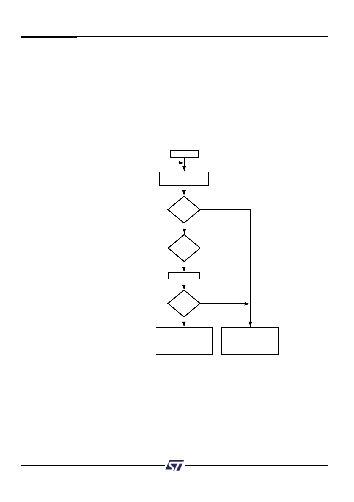
9.1.1.7.1 Data Polling
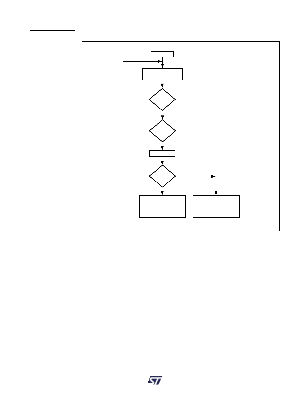
Polling on DQ7 is a method of checking whether a Program or Erase instruction is in
progress or has completed. Figure 4 shows the Data Polling algorithm.
When the MCU issues a programming instruction, the embedded algorithm within the
PSD835G2 begins. The MCU then reads the location of the word to be programmed in
Flash to check status. Data bit DQ7 of this location becomes the compliment of data
bit 7of the original data word to be programmed. The MCU continues to poll this location,
comparing DQ7 and monitoring the Error bit on DQ5. When the DQ7 matches data bit 7 of
the original data, and the Error bit at DQ5 remains ‘0’, then the embedded algorithm is
complete. If the Error bit at DQ5 is ‘1’, the MCU should test DQ7 again since DQ7 may
have changed simultaneously with DQ5 (see Figure 4).
The Error bit at DQ5 will be set if either an internal timeout occurred while the embedded
algorithm attempted to program the location or if the MCU attempted to program a ‘1’ to a
bit that was not erased (not erased is logic ‘0’).
It is suggested (as with all Flash memories) to read the location again after the embedded
programming algorithm has completed to compare the word that was written to Flash with
the word that was intended to be written.
When using the Data Polling method after an erase instruction, Figure 4 still applies.
However, DQ7 will be ‘0’ until the erase operation is complete. A ‘1’ on DQ5 will indicate
a timeout failure of the erase operation, a ‘0’ indicates no error. The MCU can read any
location within the sector being erased to get DQ7 and DQ5.
PSDsoft generates ANSI C code functions which implement these Data Polling
algorithms.
The
PSD835G2
Functional
Blocks
(cont.)
Page 24
PSD835G2 PSD8XX Family
23
Figure 4. Data Polling Flow Chart
START
READ DQ5 & DQ7
at VALID ADDRESS
YES
YES
YES
NO
NO
NO
DQ7
=
DATA7
DQ5
=1
DQ7
=
DATA
READ DQ7
FAIL
Program/Erase
Operation Failed
Issue Reset Instruction
PASS
Program/Erase
Operation is
Completed
The
PSD835G2
Functional
Blocks
(cont.)
9.1.1.7.2 Data Toggle
Checking the Data Toggle bit on DQ6 is a method of determining whether a Program or
Erase instruction is in progress or has completed. Figure 5 shows the Data Toggle
algorithm.
When the MCU issues a programming instruction, the embedded algorithm within the
PSD835G2 begins. The MCU then reads the location to be programmed in Flash to check
status. Data bit DQ6 of this location will toggle each time the MCU reads this location until
the embedded algorithm is complete. The MCU continues to read this location, checking
DQ6 and monitoring the Error bit on DQ5. When DQ6 stops toggling (two consecutive
reads yield the same value), and the Error bit on DQ5 remains ‘0’, then the embedded
algorithm is complete. If the Error bit on DQ5 is ‘1’, the MCU should test DQ6 again, since
DQ6 may have changed simultaneously with DQ5 (see Figure 5).
The Error bit at DQ5 will be set if either an internal timeout occurred while the embedded
algorithm attempted to program, or if the MCU attempted to program a ‘1’ to a bit that was
not erased (not erased is logic ‘0’).
Page 25
PSD8XX Family PSD835G2
24
9.1.1.7.2 Data Toggle (cont.)
It is suggested (as with all Flash memories) to read the location again after the embedded
programming algorithm has completed to compare the word that was written to Flash with
the word that was intended to be written.
When using the Data Toggle method after an erase instructin, Figure 5 still applies. DQ6
will toggle until the erase operation is complete. A ‘1’ on DQ5 will indicate a timeout failure
of the erase operation, a ‘0’ indicates no error. The MCU can read any even location within
the sector being erased to get DQ6 and DQ5.
PSDsoft generates ANSI C code functions which implement these Data Toggling
algorithms.
The
PSD835G2
Functional
Blocks
(cont.)
Figure 5. Data Toggle Flow Chart
START
READ
DQ5 & DQ6
NO
YES
NO
YES
YES
NO
DQ6
=
TOGGLE
DQ5
=1
DQ6
=
TOGGLE
READ DQ6
FAIL
Program/Erase
Operation Failed
Issue Reset Instruction
PASS
Program/Erase
Operation is
Completed
Page 26

PSD835G2 PSD8XX Family
25
The
PSD835G2
Functional
Blocks
(cont.)
9.1.1.8 Unlock Bypass Instruction
The unlock bypass feature allows the system to program words to the flash memories
faster than using the standard program instruction. The unlock bypass instruction is
initiated by first writing two unlock cycles. This is followed by a third write cycle containing
the unlock bypass command, 20h (see Table 8). The flash memory then enters the unlock
bypass mode. A two-cycle Unlock Bypass Program instruction is all that is required to
program in this mode. The first cycle in this instruction contains the unlock bypass
programm command, A0h; the second cycle contains the program address and data.
Additional data is programmed in the same manner. This mode dispenses with the initial
two unlock cycles required in the standard program instruction, resulting in faster total
programming time. During the unlock bypass mode, only the Unlock Bypass Program and
Unlock Bypass Reset instructions are valid. To exit the unlock bypass mode, the system
must issue the two-cycle unlock bypass reset instruction. The first cycle must contain the
data 90h; the second cycle the data 00h. Addresses are don’t care for both cycles. The
Flash memory then returns to reading array data mode.
9.1.1.9 Erasing Flash Memory
9.1.1.9.1. Flash Bulk Erase Instruction
The Flash Bulk Erase instruction uses six write operations followed by a Read operation of
the status register, as described in Table 8. If any byte of the Bulk Erase instruction is
wrong, the Bulk Erase instruction aborts and the device is reset to the Read Flash memory
status.
During a Bulk Erase, the memory status may be checked by reading status bits DQ5, DQ6,
and DQ7, as detailed in section 9.1.1.7. The Error bit (DQ5) returns a ‘1’ if there has been
an Erase Failure (maximum number of erase cycles have been executed).
It is not necessary to program the array with 00h because the PSD835G2 will automatically
do this before erasing to 0FFh.
During execution of the Bulk Erase instruction, the Flash memory will not accept any
instructions.
9.1.1.9.2 Flash Sector Erase Instruction
The Sector Erase instruction uses six write operations, as described in Table 8. Additional
Flash Sector Erase confirm commands and Flash sector addresses can be written
subsequently to erase other Flash sectors in parallel, without further coded cycles, if the
additional instruction is transmitted in a shorter time than the timeout period of about
100 µs. The input of a new Sector Erase instruction will restart the time-out period.
The status of the internal timer can be monitored through the level of DQ3 (Erase time-out
bit). If DQ3 is ‘0’, the Sector Erase instruction has been received and the timeout is
counting. If DQ3 is ‘1’, the timeout has expired and the PSD835G2 is busy erasing the
Flash sector(s). Before and during Erase timeout, any instruction other than Erase suspend
and Erase Resume will abort the instruction and reset the device to Read Array mode.
It is not necessary to program the Flash sector with 00h as the PSD835G2 will do this
automatically before erasing.
During a Sector Erase, the memory status may be checked by reading status bits DQ5,
DQ6, and DQ7, as detailed in section 9.1.1.7.
During execution of the erase instruction, the Flash block logic accepts only Reset and
Erase Suspend instructions. Erasure of one Flash sector may be suspended, in order to
read data from another Flash sector, and then resumed.
Page 27

PSD8XX Family PSD835G2
26
The
PSD835G2
Functional
Blocks
(cont.)
9.1.1.9.3 Flash Erase Suspend Instruction
When a Flash Sector Erase operation is in progress, the Erase Suspend instruction will
suspend the operation by writing 0B0h to any even address when an appropriate Chip
Select (FSi or CSBOOTi) is true. (See Table 8). This allows reading of data from another
Flash sector after the Erase operation has been suspended. Erase suspend is accepted
only during the Flash Sector Erase instruction execution and defaults to read array
mode. An Erase Suspend instruction executed during an Erase timeout will, in addition to
suspending the erase, terminate the time out.
The Toggle Bit DQ6 stops toggling when the PSD835G2 internal logic is suspended. The
toggle Bit status must be monitored at an address within the Flash sector being erased.
The Toggle Bit will stop toggling between 0.1 µs and 15 µs after the Erase Suspend
instruction has been executed. The PSD835G2 will then automatically be set to Read
Flash Block Memory Array mode.
If an Erase Suspend instruction was executed, the following rules apply:
• Attempting to read from a Flash sector that was being erased will output invalid data.
• Reading from a Flash sector that was not being erased is valid.
• The Flash memory cannot be programmed, and will only respond to Erase Resume
and Reset instructions (read is an operation and is OK).
• If a Reset instruction is received, data in the Flash sector that was being erased will
be invalid.
9.1.1.9.4 Flash Erase Resume Instruction
If an Erase Suspend instruction was previously executed, the erase operation may be
resumed by this instruction. The Erase Resume instruction consists of writing 030h to any
even address while an appropriate Chip Select (FSi or CSBOOTi) is true. (See Table 8.)
9.1.1.10 Specific Features
9.1.1.10.1 Main Flash and Secondary Flash Sector Protect
Each sector of main Flash and secondary Flash memory can be separately protected
against Program and Erase functions. Sector Protection provides additional data
security because it disables all program or erase operations. This mode can be activated
(or deactivated) through the JTAG-ISP Port or a Device Programmer.
Sector protection can be selected for each sector using the PSDsoft program. This will
automatically protect selected sectors when the device is programmed through the JTAG
Port or a Device Programmer. Flash sectors can be unprotected to allow updating of their
contents using the JTAG Port or a Device Programmer. The microcontroller can read (but
cannot change) the sector protection bits.
Any attempt to program or erase a protected Flash sector will be ignored by the device.
The Verify operation will result in a read of the protected data. This allows a guarantee of
the retention of the Protection status.
The sector protection status can either be read by the MCU through the Flash protection
and secondary Flash protection registers (CSIOP) or use the read sector protection
instruction (Table 8).
Page 28
PSD835G2 PSD8XX Family
27
The
PSD835G2
Functional
Blocks
(cont.)
Bit 7 Bit 6 Bit 5 Bit 4 Bit 3 Bit 2 Bit 1 Bit 0
Sec7_Prot Sec6_Prot Sec5_Prot Sec4_Prot Sec3_Prot Sec2_Prot Sec1_Prot Sec0_Prot
Flash Protection Register
9.1.1.10.2 Reset Instruction
The Reset instruction consists of one write cycle (see Table 8). It can also be optionally
preceded by the standard two write decoding cycles (writing AAh to AAAh and 55h to
554h).
The Reset instruction must be executed after:
1. Reading the Flash Protection status or Flash ID using the Flash instruction.
2. When an error condition occurs (DQ5 goes high) during a Flash programming or erase
cycle.
The Reset instruction will reset the Flash to normal Read Mode immediately. However, if
there is an error condition (DQ5 goes high), the Flash memory will return to the Read
Mode in 25 µSeconds after the Reset instruction is issued.
The Reset instruction is ignored when it is issued during a Flash programming or Bulk
Erase cycle. The Reset instruction will abort the on going sector erase cycle and return the
Flash memory to normal Read Mode in 25 µSeconds.
9.1.1.10.3 Reset Pin Input
The reset pulse input from the pin will abort any operation in progress and reset the Flash
memory to Read Mode. When the reset occurs during a programming or erase cycle, the
Flash memory will take up to 25 µSeconds to return to Read Mode. It is recommended that
the reset pulse (except power on reset, see Reset Section) be at least 25 µSeconds such
that the Flash memory will always be ready for the MCU to fetch the boot code after reset
is over.
Bit Definitions:
Sec<i>_Prot 1 = Main Flash Sector <i> is write protected.
Sec<i>_Prot 0 = Main Flash Sector <i> is not write protected.
Bit 7 Bit 6 Bit 5 Bit 4 Bit 3 Bit 2 Bit 1 Bit 0
Security_
***
Sec3_Prot Sec2_Prot Sec1_Prot Sec0_Prot
Bit
Flash Boot Protection Register
Bit Definitions:
Sec<i>_Prot 1 = Flash Boot Sector <i> is write protected.
Sec<i>_Prot 0 = Flash Boot Sector <i> is not write protected.
Security_Bit 0 = Security Bit in device has not been set.
1 = Security Bit in device has been set.
Table 10. Sector Protection/Security Bit Definition
*: Not used.
Page 29

PSD8XX Family PSD835G2
28
The
PSD835G2
Functional
Blocks
(cont.)
9.1.2 SRAM
The SRAM is enabled when RS0 —the SRAM chip select output from the DPLD —is high.
RS0 can contain up to three product terms, allowing flexible memory mapping.
The SRAM can be backed up using an external battery. The external battery should be
connected to the Vstby pin (PE6). If you have an external battery connected to the
PSD835G2, the contents of the SRAM will be retained in the event of a power loss. The
contents of the SRAM will be retained so long as the battery voltage remains at 2V or
greater. If the supply voltage falls below the battery voltage, an internal power switchover
to the battery occurs.
Pin PE7 can be configured as an output that indicates when power is being drawn from the
external battery. This Vbaton signal will be high with the supply voltage falls below the battery voltage and the battery on PE6 is supplying power to the internal SRAM.
The chip select signal (RS0) for the SRAM, Vstby, and Vbaton are all configured using
PSDsoft.
9.1.3 Memory Select Signals
The main Flash (FSi), secondary Flash (CSBOOTi), and SRAM (RS0) memory select
signals are all outputs of the DPLD. They are defined using PSDsoft. The following rules
apply to the equations for the internal chip select signals:
1. Main Flash memory and secondary Flash memory sector select signals must not be
larger than the physical sector size.
2. Any main Flash memory sector must not be mapped in the same memory space as
another Main Flash sector.
3. A secondary Flash memory sector must not be mapped in the same memory space as
another Flash Boot sector.
4. SRAM and I/O spaces must not overlap.
5. A secondary Flash memory sector may overlap a main Flash memory sector. In case of
overlap, priority will be given to the Flash Boot sector.
6. SRAM and I/O spaces may overlap any other memory sector. Priority will be given to
the SRAM and I/O.
Example
FS0 is valid when the address is in the range of 8000h to BFFFh, CSBOOT0 is valid from
8000h to 9FFFh, and RS0 is valid from 8000h to 87FFh. Any address in the range of RS0
will always access the SRAM. Any address in the range of CSBOOT0 greater than 87FFh
(and less than 9FFFh) will automatically address Boot memory segment 0. Any address
greater than 9FFFh will access the Flash memory segment 0. You can see that half of the
Flash memory segment 0 and one-fourth of Boot segment 0 can not be accessed in this
example. Also note that an equation that defined FS1 to anywhere in the range of 8000h to
BFFFh would not be valid.
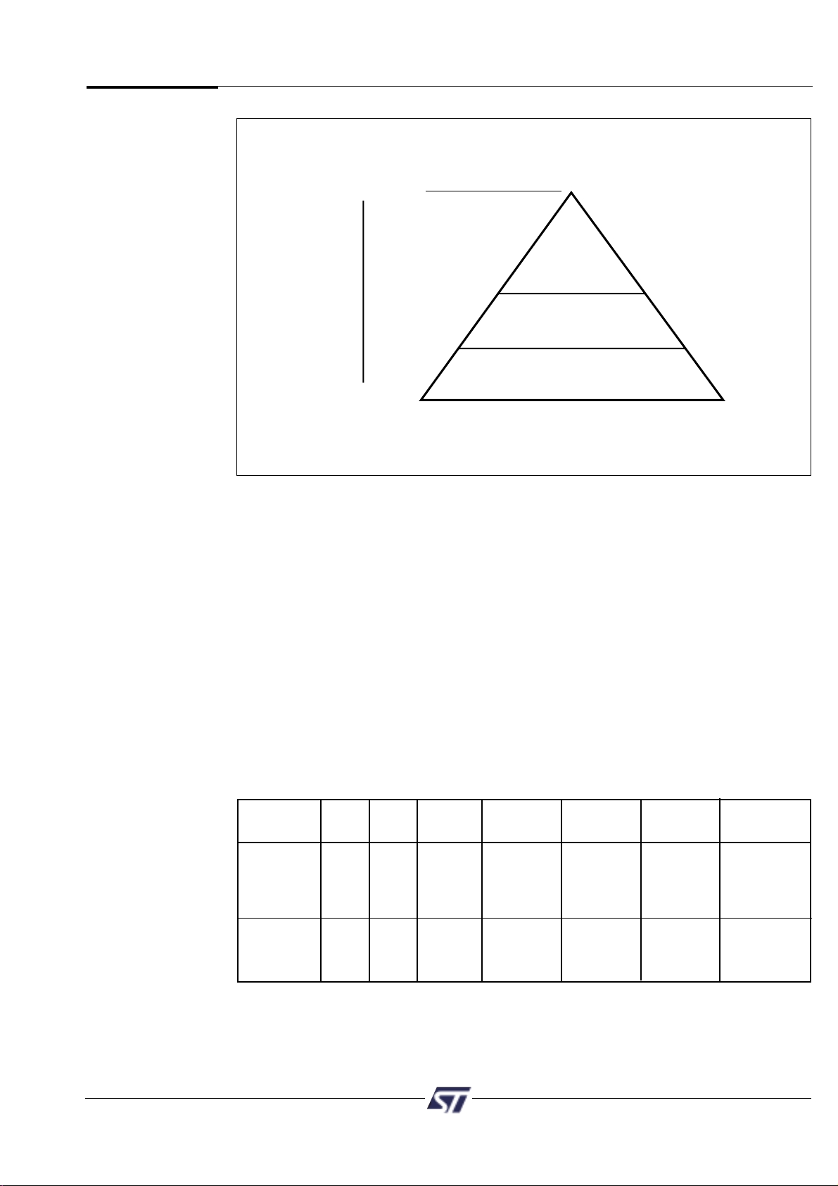
Figure 6 shows the priority levels for all memory components. Any component on a higher
level can overlap and has priority over any component on a lower level. Components on
the same level must not overlap. Level one has the highest priority and level 3 has the
lowest.
Page 30
PSD835G2 PSD8XX Family
29
The
PSD835G2
Functional
Blocks
(cont.)
Level 1
SRAM, I/O, or
Peripheral I/O
Level 2
Secondary Flash Memory
Highest Priority
Lowest Priority
Level 3
Main Flash Memory
Figure 6. Priority Level of Memory and I/O Components
9.1.3.1. Memory Select Configuration for MCUs with Separate Program and Data Spaces
The 80C51 and compatible family of microcontrollers, can be configured to have separate
address spaces for code memory (selected using PSEN) and data memory (selected using
RD). Any of the memories within the PSD835G2 can reside in either space or both spaces.
This is controlled through manipulation of the VM register that resides in the PSD’s CSIOP
space.
The VM register is set using PSDsoft to have an initial value. It can subsequently be
changed by the microcontroller so that memory mapping can be changed on-the-fly.
For example, you may wish to have SRAM and main Flash in Data Space at boot, and
secondary Flash memory in Program Space at boot, and later swap main and secondary
Flash memory. This is easily done with the VM register by using PSDsoft to configure it for
boot up and having the microcontroller change it when desired.
Table 11 describes the VM Register.
Bit 7 Bit 6* Bit 5* Bit 4 Bit 3 Bit 2 Bit 1 Bit 0
PIO_EN FL_Data Boot_Data FL_Code Boot_Code SRAM_Code
0 = disable
**
0 = RD 0 = RD 0 = PSEN 0 = PSEN 0 = PSEN
PIO mode can’t can’t can’t can’t can’t
access access access access access
Flash Boot Flash Flash Boot Flash SRAM
1= enable
**
1 = RD 1 = RD 1 = PSEN 1 = PSEN 1 = PSEN
PIO mode access access access access access
Flash Boot Flash Flash Boot Flash SRAM
Table 11. VM Register
NOTE: Bits 6-5 are not used.
Page 31

PSD8XX Family PSD835G2
30
The
PSD835G2
Functional
Blocks
(cont.)
MAIN
FLASH
DPLD
FLASH
BOOT
BLOCK
SRAM
RS0
CSBOOT0-3
FS0-7
CS CSCS
OE OE
RD
PSEN
OE
Figure 7. 80C51 Memory Modes – Separate Space Mode
MAIN
FLASH
DPLD
FLASH
BOOT
BLOCK
SRAM
RS0
CSBOOT0-3
FS0-7
RD
CS CSCS
RD
OE OE
VM REG BIT 2
PSEN
VM REG BIT 0
VM REG BIT 1
VM REG BIT 3
VM REG BIT 4
OE
Figure 8. 80C51 Memory Mode – Combined Space Mode
9.1.3.2 Configuration Modes for MCUs with Separate Program and Data Spaces
9.1.3.2.1 Separate Space Modes
Code memory space is separated from data memory space. For example, the PSEN
signal is used to access the program code from the main Flash Memory, while the RD
signal is used to access data from the secondary Flash memory, SRAM and I/O Ports.
This configuration requires the VM register to be set to 0Ch.
9.1.3.2.2 . Combined Space Modes
The program and data memory spaces are combined into one space that allows the main
Flash Memory, secondary Flash memory, and SRAM to be accessed by either PSEN or
RD. For example, to configure the main Flash memory in combined space mode, bits 2
and 4 of the VM register are set to “1”.
9.1.3.3 80C51XA Memory Map Example
See Application Notes for examples.
Page 32

PSD835G2 PSD8XX Family
31
RESET
D0-D7
R/W
D0 Q0
Q1
Q2
Q3
Q4
Q5
Q6
Q7
D1
D2
D3
D4
D5
D6
D7
PAGE
REGISTER
PGR0
PGR1
PGR2
PGR3
DPLD
AND
GPLD
INTERNAL
SELECTS
AND LOGIC
FLASH
PLD
PGR4
PGR5
PGR6
PGR7
Figure 9. Page Register
The
PSD835G2
Functional
Blocks
(cont.)
9.1.4 Page Register
The eight bit Page Register increases the addressing capability of the microcontroller by a
factor of up to 256. The contents of the register can also be read by the microcontroller.
The outputs of the Page Register (PGR0-PGR7) are inputs to the PLD decoder and
can be included in the Flash Memory, secondary Flash memory, and SRAM chip select
equations.
If memory paging is not needed, or if not all 8 page register bits are needed for memory
paging, then these bits may be used in the PLD for general logic. See Application
Notes.
Figure 9 shows the Page Register. The eight flip flops in the register are connected to the
internal data bus D0-D7. The microcontroller can write to or read from the Page Register.
The Page Register can be accessed at address location CSIOP + E0h.
Page 33

PSD8XX Family PSD835G2
32
The
PSD835G2
Functional
Blocks
(cont.)
9.1.5 Memory ID Registers
The 8-bit read only memory status registers are included in the CSIOP space. The user
can determine the memory configuration of the PSD device by reading the Memory ID0
and Memory ID1 registers. The content of the registers are defined as follow:
Bit 7 Bit 6 Bit 5 Bit 4 Bit 3 Bit 2 Bit 1 Bit 0
S_size 3 S_size 2 S_size 1 S_size 0 F_size 3 F_size 2 F_size 1 F_size 0
Memory_ID0 Register
Main Flash Size
F_size3 F_size2 F_size1 F_size0 (Bit)
0 0 0 0 none
0 0 0 1 256K
0 0 1 0 512K
00111M
01002M
01014M
01108M
Bit Definition
SRAM Size
S_size3 S_size2 S_size1 S_size0 (Bit)
0 0 0 0 none
000116K
001032K
001164K
Bit 7 Bit 6 Bit 5 Bit 4 Bit 3 Bit 2 Bit 1 Bit 0
**
B_type 1 B_type 0 B_size 3 B_size 2 B_size 1 B_size 0
Memory_ID1 Register
*Not used bit should be set to zero.
Boot Block Size
B_size3 B_size2 B_size1 B_size0 (Bit)
0 0 0 0 none
0 0 0 1 128K
0 0 1 0 256K
0 0 1 1 512K
Bit Definition
B_type1 B_type0 Boot Block Type
0 0 Flash
0 1 EEPROM
Page 34

PSD835G2 PSD8XX Family
33
The
PSD835G2
Functional
Blocks
(cont.)
9.2 PLDs
The PLDs bring programmable logic functionality to the PSD835G2. After specifying the
logic for the PLDs in PSDsoft, the logic is programmed into the device and available upon
power-up.
The PSD835G2 contains two PLDs: the Decode PLD (DPLD), and the Complex PLD
(CPLD). The PLDs are briefly discussed in the next few paragraphs, and in more detail in
sections 9.2.1 and 9.2.2. Figure 10 shows the configuration of the PLDs.
The DPLD performs address decoding for internal components, such as memory,
registers, and I/O port selects.
The CPLD can be used for logic functions, such as loadable counters and shift registers,
state machines, and encoding and decoding logic. These logic functions can be
constructed using the 16 Output Micro⇔Cells (OMCs), 24 Input Micro⇔Cells (IMCs), and
the AND array. The CPLD can also be used to generate external chip selects.
The AND array is used to form product terms. These product terms are specified using
PSDsoft. An Input Bus consisting of 82 signals is connected to the PLDs. The signals are
shown in Table 12.
Input Source Input Name Number
of Signals
MCU Address Bus A[15:0]* 16
MCU Control Signals CNTL[2:0] 3
Reset RST 1
Power Down PDN 1
Port A Input Micro⇔Cells PA[7-0] 8
Port B Input Micro⇔Cells PB[7-0] 8
Port C Input Micro⇔Cells PC[7-0] 8
Port D Inputs PD[3:0] 4
Port F Inputs PF[7:0] 8
Page Register PGR(7:0) 8
Micro⇔Cell A Feedback MCELLA.FB[7:0] 8
Micro⇔Cell B Feedback MCELLB.FB[7:0] 8
Flash Programming Status Bit Rdy/Bsy 1
Table 12. DPLD and CPLD Inputs
NOTE: The address inputs are A[19:4] in 80C51XA mode.
The Turbo Bit
The PLDs in the PSD835G2 can minimize power consumption by switching to standby
when inputs remain unchanged for an extended time of about 70 ns. Setting the Turbo
mode bit to off (Bit 3 of the PMMR0 register) automatically places the PLDs into standby if
no inputs are changing. Turbo-off mode increases propagation delays while reducing
power consumption. Refer to the Power Management Unit section on how to set the Turbo
Bit. Additionally, five bits are available in the PMMR2 register to block MCU control signals
from entering the PLDs. This reduces power consumption and can be used only when
these MCU control signals are not used in PLD logic equations.
Page 35

PSD8XX Family PSD835G2
34
PLD INPUT BUS
8
INPUT MICRO
⇔
CELL & INPUT PORTS
DIRECT MICRO
⇔
CELL INPUT TO MCU DATA BUS
CSIOP SELECT
SRAM SELECT
FLASH BOOT MEMORY SELECTS
DECODE PLD
PAGE
REGISTER
PERIPHERAL I/O MODE SELECTS
JTAG SELECT
CPLD
PT
ALLOC.
MCELLA
MCELLB
DIRECT MICRO⇔CELL ACCESS FROM MCU DATA BUS
24 INPUT MICRO
⇔
CELL
(PORT A,B,C)
16 OUTPUT
MICRO⇔CELL
I/O PORTS
FLASH MEMORY SELECTS
12
PORT D AND F INPUTS
TO PORT A
TO PORT B
DATA
BUS
8
8
8
4
1
1
2
1
EXTERNAL CHIP SELECTS
TO PORT C OR F
8
82
16
82
24
OUTPUT MICRO⇔CELL FEEDBACK
Figure 10. PLD Block Diagram
Page 36

PSD835G2 PSD8XX Family
35
The
PSD835G2
Functional
Blocks
(cont.)
Each of the two PLDs has unique characteristics suited for its applications They are
described in the following sections.
9.2.1 Decode PLD (DPLD)
The DPLD, shown in Figure 11, is used for decoding the address for internal and external
components. The DPLD can generate the following decode signals:
• 8 sector selects for the main Flash memory (three product terms each)
• 4 sector selects for the Flash Boot memory
(three product terms each)
• 1 internal SRAM select signal (three product terms)
• 1 internal CSIOP (PSD configuration register) select signal
• 1 JTAG select signal (enables JTAG-ISP on Port E)
• 2 internal peripheral select signals (peripheral I/O mode).
9.2.2 Complex PLD (CPLD)
The CPLD can be used to implement system logic functions, such as loadable counters
and shift registers, system mailboxes, handshaking protocols, state machines, and
random logic. The CPLD can also be used to generate 8 external chip selects, routed to
Port C or F. Although external chip selects can be produced by any Output Micro⇔Cell,
these eight external chip selects on Port C or F do not consume any Output Micro⇔Cells.
As shown in Figure 10, the CPLD has the following blocks:
• 24 Input Micro⇔Cells (IMCs)
• 16 Output Micro⇔Cells (OMCs)
• Product Term Allocator
• AND array capable of generating up to 196 product terms
• Four I/O ports.
Each of the blocks are described in the subsections that follow.
The Input and Output Micro⇔Cells are connected to the PSD835G2 internal data bus and
can be directly accessed by the microcontroller. This enables the MCU software to load
data into the Output Micro⇔Cells or read data from both the Input and Output
Micro⇔Cells. This feature allows efficient implementation of system logic and eliminates
the need to connect the data bus to the AND logic array as required in most standard PLD
macrocell architectures.
Page 37

PSD8XX Family PSD835G2
36
(INPUTS)
(32)
(8)
(16)
(1)
PDN (APD OUTPUT)
I/O PORTS (PORT A,B,C,F)
(8)
PGR0 -PGR7
(8)
MCELLA.FB [7:0] (FEEDBACKS)
MCELLB.FB [7:0] (FEEDBACKS)
A[15:0
]
*
(4)
(3)
PD[3:0] (ALE,CLKIN,CSI)
CNTRL[2:0
] (
READ/WRITE CONTROL SIGNALS)
(1)
(1)
RESET
RD_BSY
RS0
CSIOP
PSEL0
PSEL1
8 FLASH MEMORY
SECTOR SELECTS
4 SECONDARY
FLASH MEMORY
SECTOR SELECTS
SRAM SELECT
I/O DECODER
SELECT
PERIPHERAL I/O MODE
SELECT
CSBOOT 0
CSBOOT 1
CSBOOT 2
CSBOOT 3
FS0
FS7
3
3
3
3
3
3
3
3
3
3
3
3
3
JTAGSEL
Figure 11. DPLD Logic Array
*NOTE: 1. The address inputs are A[19:4] in 80C51XA mode.
2. Additional address lines can be brought into PSD via Port A, B, C, D or F.
Page 38

PSD835G2 Beta Information PSD8XX Family
37
I/O PORTS
CPLD MICRO
⇔
CELLS
INPUT MICRO
⇔
CELLS
LATCHED
ADDRESS OUT
MUX
MUX
MUX
MUX MUX
D
D
Q
Q
Q
G
D
QD
WR
WR
PDR
DATA
PRODUCT TERM
ALLOCATOR
DIR
REG.
SELECT
INPUT
PRODUCT TERMS
FROM OTHER
MICRO
⇔
CELLS
POLARITY
SELECT
UP TO 10
PRODUCT TERMS
CLOCK
SELECT
PR DI LD
D/T
CK
CL
Q
D/T/JK FF
SELECT
PT CLEAR
PT
CLOCK
GLOBAL
CLOCK
PT OUTPUT ENABLE
(
OE
)
MICRO
⇔
CELL FEEDBACK
I/O PORT INPUT
ALE/AS
PT INPUT LATCH GATE/CLOCK
MCU LOAD
PT PRESET
MCU DATA IN
COMB.
/REG
SELECT
PLD INPUT BUSPLD INPUT BUS
MCU ADDRESS /DATA BUS
MICRO
⇔
CELL
OUT TO
MCU
DATA
LOAD
CONTROL
AND ARRAY
PLD OUTPUT
I/O PIN
Figure 12. The Micro⇔Cell and I/O Port
Page 39

PSD8XX Family PSD835G2
38
The
PSD835G2
Functional
Blocks
(cont.)
9.2.2.1 Output Micro⇔Cell
Eight of the Output Micro⇔Cells are connected to Port A pins are named as McellA0-7.
The other eight Micro⇔Cells are connected to Port B pins are named as McellB0-7.
Maximum
Native Borrowed Data Bit for
Output Port Product Product Loading or
Micro⇔Cell Assignment Terms Terms Reading
McellA0 Port A0 3 6 D0
McellA1 Port A1 3 6 D1
McellA2 Port A2 3 6 D2
McellA3 Port A3 3 6 D3
McellA4 Port A4 3 6 D4
McellA5 Port A5 3 6 D5
McellA6 Port A6 3 6 D6
McellA7 Port A7 3 6 D7
McellB0 Port B0 4 5 D0
McellB1 Port B1 4 5 D1
McellB2 Port B2 4 5 D2
McellB3 Port B3 4 5 D3
McellB4 Port B4 4 6 D4
McellB5 Port B5 4 6 D5
McellB6 Port B6 4 6 D6
McellB7 Port B7 4 6 D7
Table 13. Output Micro⇔Cell Port and Data Bit Assignments
The Output Micro⇔Cell (OMC) architecture is shown in Figure 13. As shown in the figure,
there are native product terms available from the AND array, and borrowed product terms
available (if unused) from other OMCs. The polarity of the product term is controlled by the
XOR gate. The OMC can implement either sequential logic, using the flip-flop element, or
combinatorial logic. The multiplexer selects between the sequential or combinatorial logic
outputs. The multiplexer output can drive a Port pin and has a feedback path to the AND
array inputs.
The flip-flop in the OMC can be configured as a D, T, JK, or SR type in the PSDsoft
program. The flip-flop’s clock, preset, and clear inputs may be driven from a product term
of the AND array. Alternatively, the external CLKIN signal can be used for the clock input
to the flip-flop. The flip-flop is clocked on the rising edge of the clock input. The preset and
clear are active-high inputs. Each clear input can use up to two product terms.
Page 40

PSD835G2 PSD8XX Family
39
9.2.2.2 The Product Term Allocator
The CPLD has a Product Term Allocator. The PSDsoft uses the Allocator to borrow and
place product terms from one Micro⇔Cell to another. The following list summarizes how
product terms are allocated:
• McellA0-7 all have three native product terms and may borrow up to six more
• McellB0-3 all have four native product terms and may borrow up to five more
• McellB4-7 all have four native product terms and may borrow up to six more.
Each Micro⇔Cell may only borrow product terms from certain other Micro⇔Cells. Product
terms already in use by one Micro⇔Cell will not be available for a different Micro⇔Cell.
If an equation requires more product terms than what is available to it, then “external”
product terms will be required, which will consume other OMCs. If external product terms
are used, extra delay will be added for the equation that required the extra product terms.
This is called product term expansion. PSDsoft will perform this expansion as needed.
9.2.2.3 Loading and Reading the Output Micro⇔Cells (OMCs)
The OMCs occupy a memory location in the MCU address space, as defined by the
CSIOP (refer to the I/O section). The flip-flops in each of the 16 OMCs can be loaded from
the data bus by a microcontroller. Loading the OMCs with data from the MCU takes priority
over internal functions. As such, the preset, clear, and clock inputs to the flip-flop can be
overridden by the MCU. The ability to load the flip-flops and read them back is useful in
such applications as loadable counters and shift registers, mailboxes, and handshaking
protocols. Data is loaded to the OMCs on the trailing edge of the WR signal .
9.2.2.4 The OMC Mask Register
There is one Mask Register for each of the two groups of eight OMCs. The Mask Registers
can be used to block the loading of data to individual OMCs. The default value for the
Mask Registers is 00h, which allows loading of the OMCs. When a given bit in a Mask
Register is set to a ‘1’, the MCU will be blocked from writing to the associated OMC. For
example, suppose McellA0-3 are being used for a state machine. You would not want a
MCU write to McellA to overwrite the state machine registers. Therefore, you would want to
load the Mask Register for McellA (Mask Micro⇔Cell A) with the value 0Fh.
9.2.2.5 The Output Enable of the OMC
The OMC can be connected to an I/O port pin as a PLD output. The output enable of each
Port pin driver is controlled by a single product term from the AND array, ORed with the
Direction Register output. The pin is enabled upon power up if no output enable equation
is defined and if the pin is declared as a PLD output in PSDsoft.
If the OMC output is declared as an internal node and not as a Port pin output in the
PSDabel file, then the Port pin can be used for other I/O functions. The internal node
feedback can be routed as an input to the AND array.
The
PSD835G2
Functional
Blocks
(cont.)
Page 41

PSD8XX Family PSD835G2
40
PT
ALLOCATOR
MASK
REG.
PT CLK
PT
PT
PT
CLKIN
FEEDBACK
(
.FB
)
PORT INPUT
AND ARRAY
PLD INPUT BUS
MUX
MUX
POLARITY
SELECT
LD
IN
CLR
Q
PRDIN
COMB/REG
SELECT
PORT
DRIVER
INPUT
MICRO
⇔
CELL
I/O PIN
INTERNAL DATA BUS
DIRECTION
REGISTER
CLEAR
(
.RE
)
PROGRAMMABLE
FF
(
D/T/JK/SR
)
WR
ENABLE
(
.OE
)
PRESET
(
.PR
)
RD
MICRO
⇔
CELL CS
Figure 13. CPLD Output Micro⇔Cell
The
PSD835G2
Functional
Blocks
(cont.)
Page 42

PSD835G2 PSD8XX Family
41
9.2.2.6 Input Micro⇔Cells (IMCs)
The CPLD has 24 IMCs, one for each pin on Ports A, B, and C. The architecture of the IMC
is shown in Figure 14. The IMCs are individually configurable, and can be used as a latch,
register, or to pass incoming Port signals prior to driving them onto the PLD input bus. The
outputs of the IMCs can be read by the microcontroller through the internal data bus.
The enable for the latch and clock for the register are driven by a multiplexer whose inputs
are a product term from the CPLD AND array or the MCU address strobe (ALE/AS). Each
product term output is used to latch or clock four IMCs. Port inputs 3-0 can be controlled by
one product term and 7-4 by another.
Configurations for the IMCs are specified by PSDsoft. Outputs of the IMCs can be read by
the MCU via the IMC buffer. See the I/O Port section on how to read the IMCs.
IMCs can use the address strobe to latch address bits higher than A15. Any latched
addresses are routed to the PLDs as inputs.
IMCs are particularly useful with handshaking communication applications where two
processors pass data back and forth through a common mailbox. Figure 15 shows a typical
configuration where the Master MCU writes to the Port A Data Out Register. This, in turn,
can be read by the Slave MCU via the activation of the “Slave-Read” output enable product
term. The Slave can also write to the Port A IMCs and the Master can then read the IMCs
directly. Note that the “Slave-Read” and “Slave-Wr” signals are product terms that are
derived from the Slave MCU inputs RD, WR, and Slave_CS.
The
PSD835G2
Functional
Blocks
(cont.)
OUTPUT
MICRO
⇔CELLS A
AND
MICRO
⇔CELL B
PT
PT
FEEDBACK
AND ARRAY
PLD INPUT BUS
PORT
DRIVER
I/O PIN
INTERNAL DATA BUS
DIRECTION
REGISTER
MUX
MUX
ALE/AS
PT
Q
Q
D
D
G
LATCH
INPUT MICRO⇔CELL
ENABLE (.OE
)
D FF
INPUT MICRO
⇔
CELL_ RD
Figure 14. Input Micro⇔Cell
Page 43

PSD8XX Family PSD835G2
42
MASTER
MCU
MCU-RD
MCU-RD
MCU-WR
SLAVE–WR
SLAVE– CS
MCU-WR
D[7:0
]
D[7:0
]
CPLD
DQ
QD
PORT A
DATA OUT
REGISTER
PORT A
INPUT
MICRO⇔CELL
PORT A
SLAVE–READ
SLAVE
MCU
RD
WR
PSD835G2
Figure 15. Handshaking Communication Using Input Micro⇔Cells
The
PSD835G2
Functional
Blocks
(cont.)
9.2.2.7 External Chip Select
The CPLD also provides eight chip select outputs that can be used to select external
devices. The chip selects can be routed to either Port C or Port F, depending on the pin
declaration in the PSDsoft. Each chip select (ECS0-7) consists of one product term that can
be configured active high or low.
The output enable of the pin is controlled by either the output enable product term or the
Direction Register. (See Figure 16).
CPLD
AND
ARRAY
ECS PT
PLD INPUT BUS
PORT C OR PORT F
ECS
TO PORT C OR F
ENABLE (.OE) PT
POLARITY
BIT
DIRECTION
REGISTER
PORT PIN
Figure 16. External Chip Select
Page 44

PSD835G2 PSD8XX Family
43
The
PSD835G2
Functional
Blocks
(cont.)
9.3 Microcontroller Bus Interface
The “no-glue logic” PSD835G2 Microcontroller Bus Interface can be directly connected to
most popular microcontrollers and their control signals. Key 8-bit microcontrollers with their
bus types and control signals are shown in Table 14. The MCU interface type is
specified using the PSDsoft.
9.3.1. PSD835G2 Interface to a Multiplexed Bus
Figure 17 shows an example of a system using a microcontroller with a 8-bit multiplexed
bus and a PSD835G2. The ADIO port on the PSD835G2 is connected directly to the
microcontroller address/data bus. ALE latches the address lines internally. Latched
addresses can be brought out to Port E, F or G. The PSD835G2 drives the ADIO data bus
only when one of its internal resources is accessed and the RD input is active. Should the
system address bus exceed sixteen bits, Ports A, B, C, or F may be used as additional
address inputs.
9.3.2. PSD835G2 Interface to a Non-Multiplexed Bus
Figure 18 shows an example of a system using a microcontroller with a 8-bit
non-multiplexed bus and a PSD835G2. The address bus is connected to the ADIO Port,
and the data bus is connected to Port F. Port F is in tri-state mode when the PSD835G2
is not accessed by the microcontroller. Should the system address bus exceed sixteen
bits, Ports A, B or C may be used for additional address inputs.
Data
Bus
MCU Width CNTL0 CNTL1 CNTL2 PC7 PD0** ADIO0 PF3-PF0 PF7-PF4
8031/8051 8 WR RD PSEN * ALE A0 **
80C51XA 8 WR RD PSEN * ALE A4 A3-A0 *
80C251 8 WR PSEN **ALE A0 **
80C251 8 WR RD PSEN * ALE A0 **
80198 8 WR RD **ALE A0 **
68HC11 8 R/W E **AS A0 **
68HC05C0 8 WR RD **AS A0 **
68HC912 8 R/W E * DBE AS A0 **
Z80 8 WR RD ***A0 D3-D0 D7-D4
Z8 8 R/W DS **AS A0 **
68330 8 R/W DS **AS A0 **
M37702M2 8 R/W E **ALE A0 D3-D0 D7-D4
Table 14. Microcontrollers and their Control Signals
**Unused CNTL2 pin can be configured as PLD input. Other unused pins (PD3-0, PA3-0) can be
**configured for other I/O functions.
**ALE/AS input is optional for microcontrollers with a non-multiplexed bus
Page 45

PSD8XX Family PSD835G2
44
The
PSD835G2
Functional
Blocks
(cont.)
MICRO-
CONTROLLER
WR
RD
BHE
ALE
RESET
AD[7:0
]
A[15:8
]
A[15:8
]
A[7:0
]
ADIO
PORT
PORT
F
PORT
G
PORT
A,B, or
C
WR (CNTRL0
)
RD (CNTRL1
)
BHE (CNTRL2
)
RST
ALE (PD0
)
PORT D
(
OPTIONAL
)
A[23:16
]
(
OPTIONAL
)
(
OPTIONAL
)
PSD835G2
Figure 17. An Example of a Typical 8-Bit Multiplexed Bus Interface
MICRO-
CONTROLLER
WR
RD
BHE
ALE
RESET
D[7:0
]
A[15:0
]
A[23:16
]
D[7:0
]
ADIO
PORT
PORT
F
PORT
G
PORT
A,B or
C
WR (CNTRL0
)
RD (CNTRL1
)
BHE (CNTRL2
)
RST
ALE (PD0
)
PORT D
(OPTIONAL)
PSD835G2
Figure 18. An Example of a Typical 8-Bit Non-Multiplexed Bus Interface
Page 46

PSD835G2 PSD8XX Family
45
The
PSD835G2
Functional
Blocks
(cont.)
9.3.3 Microcontroller Interface Examples
Figures 19 through 23 show examples of the basic connections between the PSD835G2
and some popular microcontrollers. The PSD835G2 Control input pins are labeled as to
the microcontroller function for which they are configured. The MCU interface is specified
using the PSDsoft.
9.3.3.1 80C31
Figure 19 shows the interface to the 80C31, which has an 8-bit multiplexed address/data
bus. The lower address byte is multiplexed with the data bus. The microcontroller control
signals PSEN, RD, and WR may be used for accessing the internal memory components
and I/O Ports. The ALE input (pin PD0) latches the address.
9.3.3.2 80C251
The Intel 80C251 microcontroller features a user-configurable bus interface with four
possible bus configurations, as shown in Table 15.
Configuration 1 is 80C31 compatible, and the bus interface to the PSD835G2 is identical to
that shown in Figure 19. Configurations 2 and 3 have the same bus connection as shown
in Figure 20. There is only one read input (PSEN) connected to the Cntl1 pin on the
PSD835G2. The A16 connection to the PA0 pin allows for a larger address input to the
PSD835G2. Configuration 4 is shown in Figure 21. The RD signal is connected to Cntl1
and the PSEN signal is connected to the CNTL2.
The 80C251 has two major operating modes: Page Mode and Non-Page Mode. In
Non-Page Mode, the data is multiplexed with the lower address byte, and ALE is active in
every bus cycle. In Page Mode, data D[7:0] is multiplexed with address A[15:8]. In a bus
cycle where there is a Page hit, the ALE signal is not active and only addresses A[7:0]
are changing. The PSD835G2 supports both modes. In Page Mode, the PSD bus timing
is identical to Non-Page Mode except the address hold time and setup time with respect
to ALE is not required. The PSD access time is measured from address A[7:0] valid to
data in valid.
Page 47

PSD8XX Family PSD835G2
46
The
PSD835G2
Functional
Blocks
(cont.)
Configuration 80C251 Connecting to Page Mode
Read/Write PSD835G2
Pins Pins
WR CNTL0 Non-Page Mode, 80C31 compatible
1 RD CNTL1 A[7:0] multiplex with D[7:0}
PSEN CNTL2
2
WR CNTL0 Non-Page Mode
PSEN only CNTL1 A[ 7:0] multiplex with D[7:0}
3
WR CNTL0 Page Mode
PSEN only CNTL1 A[ 15:8] multiplex with D[7:0}
4
WR CNTL0 Page Mode
RD CNTL1 A[15:8] multiplex with D[7:0}
PSEN CNTL2
Table 15. 80C251 Configurations
9.3.3.3 80C51XA
The Philips 80C51XA microcontroller family supports an 8- or 16-bit multiplexed bus that
can have burst cycles. Address bits A[3:0] are not multiplexed, while A[19:4] are
multiplexed with data bits D[15:0] in 16-bit mode. In 8-bit mode, A[11:4] are multiplexed
with data bits D[7:0].
The 80C51XA can be configured to operate in eight-bit data mode. (shown in Figure 22).
The 80C51XA improves bus throughput and performance by executing Burst cycles for
code fetches. In Burst Mode, address A19-4 are latched internally by the PSD835G2, while
the 80C51XA changes the A3-0 lines to fetch up to 16 bytes of code. The PSD access
time is then measured from address A3-A0 valid to data in valid. The PSD bus timing
requirement in Burst Mode is identical to the normal bus cycle, except the address setup
and hold time with respect to ALE does not apply.
9.3.3.4 68HC11
Figure 23 shows an interface to a 68HC11 where the PSD835G2 is configured in 8-bit
multiplexed mode with E and R/W settings. The DPLD can generate the READ and WR
signals for external devices.
Page 48

PSD835G2 PSD8XX Family
47
GND
8
RESET
RESET
30 49 50 70
V
CC
92969
V
CC
V
CC
V
CC
GND GND GND GND
A[15:8]
A[15:8]
AD[7:0]
AD[7:0]
60
3
4
5
6
7
10
11
12
13
14
15
16
17
18
19
20
59
40
79
80
1
2
39
71
72
73
74
75
76
77
78
AD0
AD1
AD2
AD3
AD4
AD5
AD6
AD7
A8
A9
A10
A11
A12
A13
A14
A15
ADIO0
ADIO1
ADIO2
ADIO3
ADIO4
ADIO5
ADIO6
ADIO7
PF0
PF1
PF2
PF3
PF4
PF5
PF6
PF7
PG0
PG1
PG2
PG3
PG4
PG5
PG6
PG7
PA0
PA1
PA2
PA3
PA4
PA5
PA6
PA7
PB0
PB1
PB2
PB3
PB4
PB5
PB6
PB7
PC0
PC1
PC2
PC3
PC4
PC5
PC6
PC7
31
32
33
34
35
36
37
38
21
22
23
24
25
26
27
28
51
52
53
54
55
56
57
58
61
62
63
64
65
66
67
68
41
42
43
44
45
46
47
48
ADIO8
ADI09
ADIO10
ADIO11
ADIO12
ADIO13
ADIO14
ADIO15
CNTL0 (WR)
CNTL1 (RD)
CNTL2 (PSEN)
PD0 (ALE)
PD1 (CLKIN)
PD2 (CSI)
PD3
RESET
PE0 (TMS)
PE1 (TCK/ST)
PE2 (TDI)
PE2 (TDO)
PE4 (TSTAT/RDY)
PE5 (TERR)
PE6 (VSTBY)
PE7 (VBATON)
RESET
RESET
WR
RD
PSEN
ALE
P0.0
P0.1
P0.2
P0.3
P0.4
P0.5
P0.6
P0.7
P2.0
P2.1
P2.2
P2.3
P2.4
P2.5
P2.6
P2.7
WR
PSEN
ALE/P
39
38
37
36
35
34
33
32
21
22
23
24
25
26
27
28
16
29
30
X1
X2
RESET
INT0
INT1
T0
T1
P1.0
P1.1
P1.2
P1.3
P1.4
P1.5
P1.6
P1.7
RXD
TXD
EA/VP
19
18
9
12
13
14
15
1
2
3
4
5
6
7
8
10
11
31
CRYSTAL
80C31
RD
17
PSD835G2
Figure 19. Interfacing the PSD835G2 with an 80C31
Page 49

PSD8XX Family PSD835G2
48
GND
8
RESET
RESET
30 49 50 70
V
CC
9
A16
A17
29 69
V
CC
V
CC
V
CC
GND GND GND GND
A[17:8]
A[15:8]
AD[7:0]
AD[7:0]
*
**
3
4
5
6
7
10
11
12
13
14
15
16
17
18
19
20
59
60
40
79
80
1
2
39
71
72
73
74
75
76
77
78
A0
A1
A2
A3
A4
A5
A6
A7
AD8
AD9
AD10
AD11
AD12
AD13
AD14
AD15
ADIO0
ADIO1
ADIO2
ADIO3
ADIO4
ADIO5
ADIO6
ADIO7
PF0
PF1
PF2
PF3
PF4
PF5
PF6
PF7
PG0
PG1
PG2
PG3
PG4
PG5
PG6
PG7
PA0
PA1
PA2
PA3
PA4
PA5
PA6
PA7
PB0
PB1
PB2
PB3
PB4
PB5
PB6
PB7
PC0
PC1
PC2
PC3
PC4
PC5
PC6
PC7
31
32
33
34
35
36
37
38
21
22
23
24
25
26
27
28
51
52
53
54
55
56
57
58
61
62
63
64
65
66
67
68
41
42
43
44
45
46
47
48
ADIO8
ADIO9
ADIO10
ADIO11
ADIO12
ADIO13
ADIO14
ADIO15
CNTL0 (WR)
CNTL1 (RD)
CNTL2 (PSEN)
PD0 (ALE)
PD1 (CLKIN)
PD2 (CSI)
PD3
RESET
PE0 (TMS)
PE1 (TCK/ST)
PE2 (TDI)
PE3 (TDO)
PE4 (TSTAT/RDY)
PE5 (TERR)
PE6 (VSTBY)
PE7 (VBATON)
RESET
RESET
WR
RD
A16
A17
ALE
P0.0
P0.1
P0.2
P0.3
P0.4
P0.5
P0.6
P0.7
P2.0
P2.1
P2.2
P2.3
P2.4
P2.5
P2.6
P2.7
WR
RD/A16
PSEN
ALE
P1.0
P1.1
P1.2
P1.3
P1.4
P1.5
P1.6
P1.7
X1
X2
P3.0/RXD
P3.1/TXD
P3.2/INT0
P3.3/INT1
P3.4/T0
P3.5/T1
RESET
EA
2
3
4
5
6
7
8
9
21
20
11
13
14
15
16
17
10
35
43
42
41
40
39
38
37
36
24
25
26
27
28
29
30
31
18
19
32
33
CRYSTAL
80C251SB
PSD835G2
U1
Figure 20. Interfacing the PSD835G2 to the 80C251, with One Read Input
**Connection is optional.
**Non-page mode: AD[7:0] - ADIO[7:0].
Page 50

PSD835G2 PSD8XX Family
49
GND
8
RESET
RESET
30 49 50 70
V
CC
92969
V
CC
V
CC
V
CC
GND GND GND GND
AD[15:8]
AD[15:8]
A[7:0]
A[7:0]
**
3
4
5
6
7
10
11
12
13
14
15
16
17
18
19
20
59
40
79
80
1
2
39
71
72
73
74
75
76
77
78
A0
A1
A2
A3
A4
A5
A6
A7
AD8
AD9
AD10
AD11
AD12
AD13
AD14
AD15
ADIO0
ADIO1
ADIO2
ADIO3
ADIO4
ADIO5
ADIO6
ADIO7
PF0
PF1
PF2
PF3
PF4
PF5
PF6
PF7
PG0
PG1
PG2
PG3
PG4
PG5
PG6
PG7
PA0
PA1
PA2
PA3
PA4
PA5
PA6
PA7
PB0
PB1
PB2
PB3
PB4
PB5
PB6
PB7
PC0
PC1
PC2
PC3
PC4
PC5
PC6
PC7
31
32
33
34
35
36
37
38
21
22
23
24
25
26
27
28
51
52
53
54
55
56
57
58
61
62
63
64
65
66
67
68
41
42
43
44
45
46
47
48
ADIO8
ADI09
ADIO10
ADIO11
ADIO12
ADIO13
ADIO14
ADIO15
CNTL0 (WR)
CNTL1 (RD)
CNTL2 (PSEN)
PD0 (ALE)
PD1 (CLKIN)
PD2 (CSI)
PD3
RESET
PE0 (TMS)
PE1 (TCK/ST)
PE2 (TDI)
PE3 (TDO)
PE4 (TSTAT/RDY)
PE5 (TERR)
PE6 (VSTBY)
PE7 (VBATON)
RESET
RESET
WR
RD
ALE
P0.0
P0.1
P0.2
P0.3
P0.4
P0.5
P0.6
P0.7
P2.0
P2.1
P2.2
P2.3
P2.4
P2.5
P2.6
P2.7
WR
RD/A16
PSEN
ALE
P1.0
P1.1
P1.2
P1.3
P1.4
P1.5
P1.6
P1.7
X1
X2
P3.0/RXD
P3.1/TXD
P3.2/INT0
P3.3/INT1
P3.4/T0
P3.5/T1
RESET
EA
2
3
4
5
6
7
8
9
21
20
11
13
14
15
16
17
10
35
43
42
41
40
39
38
37
36
24
25
26
27
28
29
30
31
18
32
33
CRYSTAL
80C251SB
PSD835G2
60
19
PSEN
Figure 21. Interfacing the PSD835G2 to the 80C251, with Read and PSEN Inputs
Page 51

PSD8XX Family PSD835G2
50
GND
8
RESET
30 49 50 70
V
CC
92969
V
CC
V
CC
V
CC
GND GND GND GND
A[19:12] D[7:0]
A[3:0]
3
4
5
6
7
10
11
12
13
14
15
16
17
18
19
20
59
60
40
79
80
1
2
39
71
72
73
74
75
76
77
78
A4D0
A5D1
A6D2
A7D3
A8D4
A9D5
A10D6
A11D7
A12
A13
A14
A15
A16
A17
A18
A19
ADIO0
ADIO1
ADIO2
ADIO3
ADIO4
ADIO5
ADIO6
ADIO7
PF0
PF1
PF2
PF3
PF4
PF5
PF6
PF7
PG0
PG1
PG2
PG3
PG4
PG5
PG6
PG7
PA0
PA1
PA2
PA3
PA4
PA5
PA6
PA7
PB0
PB1
PB2
PB3
PB4
PB5
PB6
PB7
PC0
PC1
PC2
PC3
PC4
PC5
PC6
PC7
31
32
33
34
35
36
37
38
21
22
23
24
25
26
27
28
51
52
53
54
55
56
57
58
61
62
63
64
65
66
67
68
41
42
43
44
45
46
47
48
ADIO8
ADI09
ADIO10
ADIO11
ADIO12
ADIO13
ADIO14
ADIO15
CNTL0 (WR)
CNTL1 (RD)
CNTL2 (PSEN)
PD0 (ALE)
PD1 (CLKIN)
PD2 (CSI)
PD3
RESET
PE0 (TMS)
PE1 (TCK/ST)
PE2 (TDI)
PE3 (TDO)
PE4 (TSTAT/RDY)
PE5 (TERR)
PE6 (VSTBY)
PE7 (VBATON)
RESET
WRRESET
RD
A3
A2
A1
A0
V
CC
PSEN
ALE
A0
A1
A2
A3
A4D0
A5D1
A6D2
A7D3
A8D4
A9D5
A10D6
A11D7
A12D8
A13D9
A14D10
A15D11
A16D12
A17D13
A18D14
A19D15
A3
A2
A1
A0/WRH
WRL
RD
PSEN
ALE
43
42
41
40
39
38
37
36
24
25
26
27
28
29
30
31
5
4
3
2
18
19
32
33
XTAL1
XTAL2
RXD0
TXD0
RXD1
TXD1
T2EX
T2
T0
RST
INT0
INT1
EA/WAIT
BUSW
21
20
11
13
6
7
9
8
16
10
14
15
35
17
CRYSTAL
XA-G3
PSD835G2
Figure 22. Interfacing the PSD835G2 to the 80C51XA, 8-Bit Data Bus
Page 52

PSD835G2 PSD8XX Family
51
GND
8
RESET
30 49 50 70
V
CC
92969
V
CC
V
CC
V
CC
GND GND GND GND
A[15:8]
A[15:8]
AD[7:0]
AD[7:0]
3
4
5
6
7
10
11
12
13
14
15
16
17
18
19
20
59
60
40
79
80
1
2
39
71
72
73
74
75
76
77
78
AD0
AD1
AD2
AD3
AD4
AD5
AD6
AD7
A8
A9
A10
A11
A12
A13
A14
A15
ADIO0
ADIO1
ADIO2
ADIO3
ADIO4
ADIO5
ADIO6
ADIO7
PF0
PF1
PF2
PF3
PF4
PF5
PF6
PF7
PG0
PG1
PG2
PG3
PG4
PG5
PG6
PG7
PA0
PA1
PA2
PA3
PA4
PA5
PA6
PA7
PB0
PB1
PB2
PB3
PB4
PB5
PB6
PB7
PC0
PC1
PC2
PC3
PC4
PC5
PC6
PC7
31
32
33
34
35
36
37
38
21
22
23
24
25
26
27
28
51
52
53
54
55
56
57
58
61
62
63
64
65
66
67
68
41
42
43
44
45
46
47
48
ADIO8
ADIO9
ADIO10
ADIO11
ADIO12
ADIO13
ADIO14
ADIO15
CNTL0 (R/W)
CNTL1 (E)
CNTL2
PD0 (AS)
PD1 (CLKIN)
PD2 (CSI)
PD3
RESET
PE0 (TMS)
PE1 (TCK/ST)
PE2 (TDI)
PE3 (TDO)
PE4 (TSTAT/RDY)
PE5 (TERR)
PE6 (VSTBY)
PE7 (VBATON)
RESET
RESET
RW
E
AS
PC0
PC1
PC2
PC3
PC4
PC5
PC6
PC7
PB0
PB1
PB2
PB3
PB4
PB5
PB6
PB7
RW
E
AS
RESET
PA0
PA1
PA2
PA3
PA4
PA5
PA6
PA7
XT
EX
IRQ
XIRQ
PD0
PD1
PD2
PD3
PD4
PD5
PE0
PE1
PE2
PE3
PE4
PE5
PE6
PE7
VRH
VRL
MODB
MODA
34
33
32
31
30
29
28
27
8
7
19
18
20
21
22
23
24
25
43
45
47
49
44
46
48
50
52
51
2
3
9
10
11
12
13
14
15
16
42
41
40
39
38
37
36
35
6
5
4
17
CRYSTAL
68HC11E9
PSD835G2
Figure 23. Interfacing the PSD835G2 with a 68HC11
Page 53

PSD8XX Family PSD835G2
52
The
PSD835G2
Functional
Blocks
(cont.)
9.4 I/O Ports
There are seven programmable I/O ports: Ports A, B, C, D, E, F and G. Each of the ports
is eight bits except Port D, which is 4 bits. Each port pin is individually user configurable,
thus allowing multiple functions per port. The ports are configured using PSDsoft or by the
microcontroller writing to on-chip registers in the CSIOP address space.
The topics discussed in this section are:
• General Port Architecture
• Port Operating Modes
• Port Configuration Registers
• Port Data Registers
• Individual Port Functionality.
9.4.1 General Port Architecture
The general architecture of the I/O Port is shown in Figure 24. Individual Port architectures
are shown in Figures 26 through 28. In general, once the purpose for a port pin has been
defined, that pin will no longer be available for other purposes. Exceptions will be noted.
As shown in Figure 24, the ports contain an output multiplexer whose selects are driven
by the configuration bits in the Control Registers (Ports E, F and G only) and PSDsoft
Configuration. Inputs to the multiplexer include the following:
❏ Output data from the Data Out Register
❏ Latched address outputs
❏ CPLD Micro⇔Cell output
❏ External Chip Select from CPLD.
The Port Data Buffer (PDB) is a tri-state buffer that allows only one source at a time to be
read. The PDB is connected to the Internal Data Bus for feedback and can be read by the
microcontroller. The Data Out and Micro⇔Cell outputs, Direction and Control Registers,
and port pin input are all connected to the PDB.
The Port pin’s tri-state output driver enable is controlled by a two input OR gate whose
inputs come from the CPLD AND array enable product term and the Direction Register. If
the enable product term of any of the array outputs are not defined and that port pin is not
defined as a CPLD output in the PSDabel file, then the Direction Register has sole control
of the buffer that drives the port pin.
The contents of these registers can be altered by the microcontroller. The PDB feedback
path allows the microcontroller to check the contents of the registers.
Ports A, B, and C have embedded Input Micro⇔Cells (IMCs). The IMCs can be configured
as latches, registers, or direct inputs to the PLDs. The latches and registers are clocked by
the address strobe (AS/ALE) or a product term from the PLD AND array. The outputs from
the IMCs drive the PLD input bus and can be read by the microcontroller. Refer to the IMC
subsection of the PLD section.
Page 54

PSD835G2 PSD8XX Family
53
INTERNAL DATA BUS
DATA OUT
REG.
DQ
D
G
Q
DQ
DQ
WR
WR
WR
ADDRESS
MICRO⇔CELL OUTPUTS
ENABLE PRODUCT TERM (.OE
)
EXT CS
ALE
READ MUX
P
D
B
CPLD-INPUT
CONTROL REG.
DIR REG.
INPUT
MICRO⇔CELL
ENABLE OUT
DATA IN
OUTPUT
SELECT
OUTPUT
MUX
PORT PIN
DATA OUT
ADDRESS
Figure 24. General I/O Port Architecture
The
PSD835G2
Functional
Blocks
(cont.)
Page 55

PSD8XX Family PSD835G2
54
The
PSD835G2
Functional
Blocks
(cont.)
9.4.2 Port Operating Modes
The I/O Ports have several modes of operation. Some modes can be defined using
PSDsoft, some by the microcontroller writing to the Registers in CSIOP space, and some
by both. The modes that can only be defined using PSDsoft must be programmed into the
device and cannot be changed unless the device is reprogrammed. The modes that can be
changed by the microcontroller can be done so dynamically at run-time. The PLD I/O,
Data Port, Address Input, Peripheral I/O and MCU Reset modes are the only modes that
must be defined before programming the device. All other modes can be changed by the
microcontroller at run-time.
Table 16 summarizes which modes are available on each port. Table 17 shows how and
where the different modes are configured. Each of the port operating modes are described
in the following subsections.
Port Mode Port A Port B Port C Port D Port E Port F Port G
MCU I/O Yes Yes Yes Yes Yes Yes Yes
PLD I/O
McellA Outputs Yes No No No No No No
McellB Outputs No Yes No No No No No
Additional Ext. CS Outputs No No Yes No No Yes No
PLD Inputs Yes Yes Yes Yes No Yes No
Address Out No No No No Yes Yes Yes
(A7-0) (A7-0) (A7-0)
or
(A15-8)
Address In Yes Yes Yes Yes No Yes No
Data Port No No No No No Yes No
Peripheral I/O No No No No No Yes No
JTAG ISP No No No No Yes* No No
Table 16. Port Operating Modes
*Can be multiplexed with other I/O functions.
Page 56

PSD835G2 PSD8XX Family
55
The
PSD835G2
Functional
Blocks
(cont.)
Control Direction VM
Defined In Register Register Register JTAG
Mode PSDsoft Setting Setting Setting Enable
Declare
0
1= output,
MCU I/O
pins only
(Note 3)
0= input NA NA
(Note 1)
Declare pins
PLD I/O and logic NA (Note 1) NA NA
equations
Data Port
Selected for
(Port F)
MCU with NA NA NA NA
non-mux bus
Address Out Declare
1 1 (Note 1) NA NA
(Port E, F, G) pins only
Declare pins or
Address In logic equation
NA NA NA NA
(Port A,B,C,D,F) for input
Micro⇔Cells
Peripheral I/O Logic equations NA NA PIO bit =1 NA
(Port F) (PSEL0 & 1)
JTAG ISP Declare pins
NA NA NA JTAG_Enable
(Note 2) only
Table 17. Port Operating Mode Settings
*NA = Not Applicable
NOTE: 1. The direction of the Port A,B,C, and F pins are controlled by the Direction Register ORed with the
individual output enable product term (.oe) from the CPLD AND array.
2. Any of these three methods will enable JTAG pins on Port E.
3. Control Register setting is not applicable to Ports A, B and C.
9.4.2.1 MCU I/O Mode
In the MCU I/O Mode, the microcontroller uses the PSD835G2 ports to expand its own
I/O ports. By setting up the CSIOP space, the ports on the PSD4000 are mapped into the
microcontroller address space. The addresses of the ports are listed in Table 6.
A port pin can be put into MCU I/O mode by writing a ‘0’ to the corresponding bit in the
Control Register (Port E, F and G). The MCU I/O direction may be changed by writing to
the corresponding bit in the Direction Register, or by the output enable product term. See
the subsection on the Direction Register in the “Port Registers” section. When the pin is
configured as an output, the content of the Data Out Register drives the pin. When configured as an input, the microcontroller can read the port input through the Data In buffer.
See Figure 22.
Ports A, B and C do not have Control Registers, and are in MCU I/O mode by default.
They can be used for PLD I/O if they are specified in PSDsoft.
9.4.2.2 PLD I/O Mode
The PLD I/O Mode uses a port as an input to the CPLD’s Input Micro⇔Cells, and/or as an
output from the CPLD’s Output Micro⇔Cells. The output can be tri-stated with a control
signal. This output enable control signal can be defined by a product term from the PLD, or
by setting the corresponding bit in the Direction Register to ‘0’. The corresponding bit in the
Direction Register must not be set to ‘1’ if the pin is defined as a PLD input pin in PSDsoft.
The PLD I/O Mode is specified in PSDsoft by declaring the port pins, and then specifying
an equation in PSDsoft.
Page 57

PSD8XX Family PSD835G2
56
The
PSD835G2
Functional
Blocks
(cont.)
MCU Port E (3:0) Port E (7:4) Port F (3:0) Port F (7:4) Port G (3:0) Port G (7:4)
80C51XA N/A* Addr (7:4) N/A* Addr (7:4) Addr (11:8) N/A
80C251
N/A N/A N/A N/A Addr (11:8) Addr (15:12)
(Page Mode)
All Other
Eight-Bit Addr (3:0) Addr (7:4) Addr (3:0) Addr (7:4) Addr (3:0) Addr (7:4)
Multiplexed
8-Bit
Non-Mux N/A N/A N/A N/A Addr (3:0) Addr (7:4)
Bus
Table 18. I/O Port Latched Address Output Assignments
9.4.2.4 Address In Mode
For microcontrollers that have more than 16 address lines, the higher addresses can be
connected to Ports A, B, C, D or F and are routed as inputs to the PLDs. The address
input can be latched in the Input Micro⇔Cell by the address strobe (ALE/AS). Any
input that is included in the DPLD equations for the Main Flash, Boot Flash, or SRAM is
considered to be an address input.
9.4.2.5 Data Port Mode
Port F can be used as a data bus port for a microcontroller with a non-multiplexed
address/data bus. The Data Port is connected to the data bus of the microcontroller. The
general I/O functions are disabled in Port F if the ports are configured as Data Port. Data
Port Mode is automatically configured in PSDsoft when a non-multiplexed bus MCU is
selected.
9.4.2.6 Peripheral I/O Mode
Peripheral I/O Mode can be used to interface with external 8-bit peripherals. In this mode,
all of Port F serves as a tri-stateable, bi-directional data buffer for the microcontroller.
Peripheral I/O Mode is enabled by setting Bit 7 of the VM Register to a ‘1’. Figure 25
shows how Port A acts as a bi-directional buffer for the microcontroller data bus if
Peripheral I/O Mode is enabled. An equation for PSEL0 and/or PSEL1 must be specified in
PSDsoft. The buffer is tri-stated when PSEL 0 or 1 is not active.
9.4.2.7 JTAG ISP
Port E is JTAG compliant, and can be used for In-System Programming (ISP). You can
multiplex JTAG operations with other functions on Port E because ISP is not performed
during normal system operation. For more information on the JTAG Port, refer to
section 9.6.
9.4.2.3 Address Out Mode
For microcontrollers with a multiplexed address/data bus, Address Out Mode can be used
to drive latched addresses onto the port pins. These port pins can, in turn, drive external
devices. Either the output enable or the corresponding bits of both the Direction Register
and Control Register must be set to a ‘1’ for pins to use Address Out Mode. This must be
done by the MCU at run-time. See Table 18 for the address output pin assignments on
Ports E, F and F for various MCUs.
Note: Do not drive address lines with Address Out Mode to an external memory device if
it is intended for the MCU to boot from the external device. The MCU must first boot from
PSD memory so the Direction and Control register bits can be set.
Page 58

PSD835G2 PSD8XX Family
The
PSD835G2
Functional
Blocks
(cont.)
57
RD
PSEL0
PSEL1
PSEL
VM REGISTER BIT 7
WR
PF0- PF7
D0-D7
DATA BUS
Figure 25. Peripheral I/O Mode
9.4.3 Port Configuration Registers (PCRs)
Each port has a set of PCRs used for configuration. The contents of the registers can be
accessed by the microcontroller through normal read/write bus cycles at the addresses
given in Table 6. The addresses in Table 6 are the offsets in hex from the base of the
CSIOP register.
The pins of a port are individually configurable and each bit in the register controls its
respective pin. For example, Bit 0 in a register refers to Bit 0 of its port. The three PCRs,
shown in Table 22, are used for setting the port configurations. The default power-up state
for each register in Table 19 is 00h.
Register Name Port MCU Access
Control E,F,G Write/Read
Direction A,B,C,D,E,F,G Write/Read
Drive Select* A,B,C,D,E,F,G Write/Read
Table 19. Port Configuration Registers
*NOTE: See Table 26 for Drive Register bit definition.
Page 59

PSD8XX Family PSD835G2
58
The
PSD835G2
Functional
Blocks
(cont.)
9.4.3.1 Control Register
Any bit set to ‘0’ in the Control Register sets the corresponding Port pin to MCU I/O Mode,
and a ‘1’ sets it to Address Out Mode. The default mode is MCU I/O. Only Ports E, F and
G have an associated Control Register.
9.4.3.2 Direction Register
The Direction Register controls the direction of data flow in the I/O Ports. Any bit set to ‘1’
in the Direction Register will cause the corresponding pin to be an output, and any bit set
to ‘0’ will cause it to be an input. The default mode for all port pins is input.
Figures 26 and 28 show the Port Architecture diagrams for Ports A/B/C and E/F/G
respectively. The direction of data flow for Ports A, B, C and F are controlled not only by
the direction register, but also by the output enable product term from the PLD AND array.
If the output enable product term is not active, the Direction Register has sole control of a
given pin’s direction.
An example of a configuration for a port with the three least significant bits set to output
and the remainder set to input is shown in Table 22. Since Port D only contains four pins,
the Direction Register for Port D has only the four least significant bits active.
Direction Register Bit Port Pin Mode
0 Input
1 Output
Table 20. Port Pin Direction Control,
Output Enable P.T. Not Defined
Direction Register Bit Output Enable P.T. Port Pin Mode
0 0 Input
0 1 Output
1 0 Output
1 1 Output
Table 21. Port Pin Direction Control, Output Enable P.T. Defined
Bit 7 Bit 6 Bit 5 Bit 4 Bit 3 Bit 2 Bit 1 Bit 0
00000111
Table 22. Port Direction Assignment Example
Page 60

PSD835G2 PSD8XX Family
59
The
PSD835G2
Functional
Blocks
(cont.)
Drive
Bit 7 Bit 6 Bit 5 Bit 4 Bit 3 Bit 2 Bit 1 Bit 0
Register
Port A
Open Open Open Open Open Open Open Open
Drain Drain Drain Drain Drain Drain Drain Drain
Port B
Open Open Open Open Open Open Open Open
Drain Drain Drain Drain Drain Drain Drain Drain
Port C
Slew Slew Slew Slew Slew Slew Slew Slew
Rate Rate Rate Rate Rate Rate Rate Rate
Port D
Open Open Open Open
Drain Drain Drain Drain
Port E
Open Open Open Open Open Open Open Open
Drain Drain Drain Drain Drain Drain Drain Drain
Port F
Slew Slew Slew Slew Slew Slew Slew Slew
Rate Rate Rate Rate Rate Rate Rate Rate
Port G
Open Open Open Open Open Open Open Open
Drain Drain Drain Drain Drain Drain Drain Drain
Table 23. Drive Register Pin Assignment
9.4.3.3 Drive Select Register
The Drive Select Register configures the pin driver as Open Drain or CMOS for some port
pins, and controls the slew rate for the other port pins. An external pull-up resistor should
be used for pins configured as Open Drain.
A pin can be configured as Open Drain if its corresponding bit in the Drive Select Register
is set to a ‘1’. The default pin drive is CMOS.
Aside: the slew rate is a measurement of the rise and fall times of an output. A higher
slew rate means a faster output response and may create more electrical noise. A pin
operates in a high slew rate when the corresponding bit in the Drive Register is set to ‘1’.
The default rate is slow slew.
Table 23 shows the Drive Register for Ports A, B, C, D, E, F and G. It summarizes which
pins can be configured as Open Drain outputs and which pins the slew rate can be set for.
Page 61

PSD8XX Family PSD835G2
60
The
PSD835G2
Functional
Blocks
(cont.)
9.4.4 Port Data Registers
The Port Data Registers, shown in Table 24, are used by the microcontroller to write data
to or read data from the ports. Table 24 shows the register name, the ports having each
register type, and microcontroller access for each register type. The registers are
described below.
9.4.4.1 Data In
Port pins are connected directly to the Data In buffer. In MCU I/O input mode, the pin input
is read through the Data In buffer.
9.4.4.2 Data Out Register
Stores output data written by the MCU in the MCU I/O output mode. The contents of the
Register are driven out to the pins if the Direction Register or the output enable
product term is set to “1”. The contents of the register can also be read back by the
microcontroller.
9.4.4.3 Output Micro⇔Cells (OMCs)
The CPLD OMCs occupy a location in the microcontroller’s address space. The
microcontroller can read the output of the OMCs. If the Mask Micro⇔Cell Register bits are
not set, writing to the Micro⇔Cell loads data to the Micro⇔Cell flip flops. Refer to the PLD
section for more details.
9.4.4.4 Mask Micro⇔Cell Register
Each Mask Register bit corresponds to an OMC flip flop. When the Mask Register bit
is set to a “1”, loading data into the OMC flip flop is blocked. The default value is “0” or
unblocked.
9.4.4.5 Input Micro⇔Cells (IMCs)
The IMCs can be used to latch or store external inputs. The outputs of the IMCs
are routed to the PLD input bus, and can be read by the microcontroller. Refer to the PLD
section for a detailed description.
9.4.4.6 Enable Out
The Enable Out register can be read by the microcontroller. It contains the output enable
values for a given port. A “1” indicates the driver is in output mode. A “0” indicates the
driver is in tri-state and the pin is in input mode.
Register Name Port MCU Access
Data In A,B,C,D,E,F,G Read – input on pin
Data Out A,B,C,D,E,F,G Write/Read
Output Micro⇔Cell A,B Read – outputs of Micro⇔Cells
Write – loading Micro⇔Cells Flip-Flop
Mask Micro⇔Cell A,B Write/Read – prevents loading into a given
Micro⇔Cell
Input Micro⇔Cell A,B,C Read – outputs of the Input Micro⇔Cells
Enable Out A,B,C,F Read – the output enable control of the port driver
Table 24. Port Data Registers
Page 62

PSD835G2 PSD8XX Family
61
9.4.5 Ports A, B and C – Functionality and Structure
Ports A and B have similar functionality and structure, as shown in Figure 26. The two
ports can be configured to perform one or more of the following functions:
❏ MCU I/O Mode
❏ CPLD Output – Micro⇔Cells McellA[7:0] can be connected to Port A.
McellB[7:0] can be connected to Port B.
External chip select ECS [7:0] can be connected to Port C.
❏ CPLD Input – Via the input Micro⇔Cells.
❏ Address In – Additional high address inputs using the Input Micro⇔Cells.
❏ Open Drain/Slew Rate – pins PC[7:0]can be configured to fast slew rate,
pins PA[7:0] and PB[7:0] can be configured to Open Drain
Mode.
INTERNAL DATA BUS
DATA OUT
REG.
DQ
DQ
WR
WR
MCELLB
[
7:0
] (PORT B)
MCELLA
[
7:0
] (PORT A)
EXT.CS (PORT C)
ENABLE PRODUCT TERM
(
.OE
)
READ MUX
P
D
B
CPLD-INPUT
DIR REG.
INPUT
MICRO
⇔
CELL
ENABLE OUT
DATA IN
OUTPUT
SELECT
OUTPUT
MUX
PORT PIN
DATA OUT
Figure 26. Port A, B and C
The
PSD835G2
Functional
Blocks
(cont.)
Page 63

PSD8XX Family PSD835G2
62
9.4.6 Port D – Functionality and Structure
Port D has four I/O pins. See Figure 27. Port D can be configured to program one more of
the following functions:
❏ MCU I/O Mode
❏ CPLD Input – direct input to CPLD, no Input Micro⇔Cells
Port D pins can be configured in PSDsoft as input pins for other dedicated functions:
❏ PD0 – ALE, as address strobe input
❏ PD1 – CLKIN, as clock input to the Micro⇔Cells Flip Flops and APD counter
❏ PD2 – CSI, as active low chip select input. A high input will disable the
Flash/SRAM and CSIOP.
❏ PD3 – as DBE input from 68HC912
9.4.7 Port E – Functionality and Structure
Port E can be configured to perform one or more of the following functions (see Figure 28):
❏ MCU I/O Mode
❏ In-System Programming – JTAG port can be enabled for programming/erase of the
PSD8XX device. (See Section 9.6 for more information on JTAG programming.)
❏ Open Drain – Port E pins can be configured in Open Drain Mode
❏ Battery Backup features – PE6 can be configured as a Battery Input (Vstby) pin.
PE7 can be configured as a Battery On Indicator output
pin, indicating when Vcc is less than Vbat.
❏ Latched Address Output – Provided latched address (A7-0) output
INTERNAL DATA BUS
DATA OUT
REG.
DQ
DQ
WR
WR
READ MUX
P
D
B
CPLD-INPUT
DIR REG.
DATA IN
OUTPUT
SELECT
OUTPUT
MUX
PORT D PIN
DATA OUT
Figure 27. Port D Structure
The
PSD835G2
Functional
Blocks
(cont.)
Page 64

PSD835G2 PSD8XX Family
63
The
PSD4000
Functional
Blocks
(cont.)
INTERNAL DATA BUS
DATA OUT
REG.
DQ
DGQ
DQ
DQ
WR
WR
WR
ADDRESS
EXT. CS (PORT F)
ENABLE PRODUCT TERM (.OE
)
ALE
READ MUX
P
D
B
CONTROL REG.
DIR REG.
ENABLE OUT
CPLD INPUT (PORT F)
ISP OR BATTERY BACK-UP (PORT E)
DATA IN
OUTPUT
SELECT
OUTPUT
MUX
PORT PIN
DATA OUT
ADDRESS
A[7:0] OR A[15:8
]
CONFIGURATION
BIT
Figure 28. Ports E, F and G Structure
9.4.8 Port F – Functionality and Structure
Port F can be configured to perform one or more of the following functions:
❏ MCU I/O Mode
❏ CPLD Output – external chip select ECS[7:0] can be connected to Port F (or Port C).
❏ CPLD Input – as direct input ot the CPLD array.
❏ Address In – additional high address inputs. Direct input to the CPLD array, no Input
Micro⇔Cells latching is available.
❏ Latched Address Out – Provide latched address out per Table 29.
❏ Slew Rate – pins can be set up for fast slew rate.
❏ Data Port – connected to D[7:0] when Port F is configured as Data Port for a
non-multiplexed bus.
❏ Peripheral I/O Mode
9.4.9 Port G – Functionality and Structure
Port G can be configured to perform one or more of the following functions:
❏ MCU I/O Mode
❏ Latched Address Out – provide latched address out per Table 29.
❏ Open Drain – pins can be configured in Open Drain Mode
Page 65

PSD8XX Family PSD835G2
64
9.5 Power Management
The PSD835G2 offers configurable power saving options. These options may be used
individually or in combinations, as follows:
❏ All memory types in a PSD (Flash, Secondary Flash, and SRAM) are built with
Zero-Power technology. In addition to using special silicon design methodology,
Zero-Power technology puts the memories into standby mode when address/data
inputs are not changing (zero DC current). As soon as a transition occurs on an input,
the affected memory “wakes up”, changes and latches its outputs, then goes back to
standby. The designer does not have to do anything special to achieve memory
standby mode when no inputs are changing—it happens automatically.
The PLD sections can also achieve standby mode when its inputs are not changing,
see PMMR registers below.
❏ Like the Zero-Power feature, the Automatic Power Down (APD) logic allows the PSD to
reduce to standby current automatically. The APD will block MCU address/data signals
from reaching the memories and PLDs. This feature is available on all PSD835G2
devices. The APD unit is described in more detail in section 9.5.1.
Built in logic will monitor the address strobe of the MCU for activity. If there is no
activity for a certain time period (MCU is asleep), the APD logic initiates Power Down
Mode (if enabled). Once in Power Down Mode, all address/data signals are blocked
from reaching PSD memories and PLDs, and the memories are deselected internally.
This allows the memories and PLDs to remain in standby mode even if the
address/data lines are changing state externally (noise, other devices on the MCU
bus, etc.). Keep in mind that any unblocked PLD input signals that are changing states
keeps the PLD out of standby mode, but not the memories.
❏ The PSD Chip Select Input (CSI) can be used to disable the internal memories,
placing them in standby mode even if inputs are changing. This feature does not block
any internal signals or disable the PLDs. This is a good alternative to using the APD
logic, especially if your MCU has a chip select output. There is a slight penalty in
memory access time when the CSI signal makes its initial transition from deselected
to selected.
❏ The PMMR registers can be written by the MCU at run-time to manage power. All PSD
devices support “blocking bits” in these registers that are set to block designated
signals from reaching both PLDs. Current consumption of the PLDs is directly related
to the composite frequency of the changes on their inputs (see Figures 32 and 32a).
Significant power savings can be achieved by blocking signals that are not used in
PLD logic equations at run time. PSDsoft creates a fuse map that automatically blocks
the low address byte (A7-A0) or the control signals (CNTL0-2, ALE and WRH/DBE) if
none of these signals are used in PLD logic equations.
The PSD835G2 devices have a Turbo Bit in the PMMR0 register. This bit can be set
to disable the Turbo Mode feature (default is Turbo Mode on). While Turbo Mode is
disabled, the PLDs can achieve standby current when no PLD inputs are changing
(zero DC current). Even when inputs do change, significant power can be saved at
lower frequencies (AC current), compared to when Turbo Mode is enabled. Conversely,
when the Turbo Mode is enabled, there is a significant DC current component and the
AC component is higher.
9.5.1 Automatic Power Down (APD) Unit and Power Down Mode
The APD Unit, shown in Figure 24, puts the PSD into Power Down Mode by monitoring
the activity of the address strobe (ALE/AS). If the APD unit is enabled, as soon as activity
on the address strobe stops, a four bit counter starts counting. If the address strobe
remains inactive for fifteen clock periods of the CLKIN signal, the Power Down (PDN)
signal becomes active, and the PSD will enter into Power Down Mode, discussed next.
The
PSD835G2
Functional
Blocks
(cont.)
Page 66

PSD835G2 PSD8XX Family
65
The
PSD835G2
Functional
Blocks
(cont.)
Access 5V VCC,
PLD Memory Recovery Time Typical
Propagation Access to Normal Standby
Mode Delay Time Access Current
Power Down
Normal t pd
No Access tLVDV
50 µA
(Note 1) (Note 2)
Table 26. PSD835G2 Timing and Standby Current During Power
Down Mode
NOTES: 1. Power Down does not affect the operation of the PLD. The PLD operation in this
mode is based only on the Turbo Bit.
2. Typical current consumption assuming no PLD inputs are changing state and
the PLD Turbo bit is off.
Port Function Pin Level
MCU I/O No Change
PLD Out No Change
Address Out Undefined
Data Port Three-State
Peripheral I/O Three-State
Table 25. Power Down Mode’s Effect on
Ports
9.5.1 Automatic Power Down (APD) Unit and Power Down Mode (cont.)
Power Down Mode
By default, if you enable the PSD APD unit, Power Down Mode is automatically enabled.
The device will enter Power Down Mode if the address strobe (ALE/AS) remains inactive
for fifteen CLKIN (pin PD1) clock periods.
The following should be kept in mind when the PSD is in Power Down Mode:
• If the address strobe starts pulsing again, the PSD will return to normal operation.
The PSD will also return to normal operation if either the CSI input returns low or the
Reset input returns high.
• The MCU address/data bus is blocked from all memories and PLDs.
• Various signals can be blocked (prior to Power Down Mode) from entering the PLDs
by setting the appropriate bits in the PMMR registers. The blocked signals include
MCU control signals and the common clock (CLKIN). Note that blocking CLKIN from
the PLDs will not block CLKIN from the APD unit.
• All PSD memories enter Standby Mode and are drawing standby current. However,
the PLDs and I/O ports do not go into Standby Mode because you don’t want to
have to wait for the logic and I/O to “wake-up” before their outputs can change. See
Table 25 for Power Down Mode effects on PSD ports.
• Typical standby current is 50 µA for 5 V parts. This standby current value assumes
that there are no transitions on any PLD input.
Page 67

PSD8XX Family PSD835G2
66
APD EN
PMMR0 BIT 1=1
ALE
RESET
CSI
CLKIN
TRANSITION
DETECTION
EDGE
DETECT
APD
COUNTER
POWER DOWN
(
PDN
)
DISABLE BUS
INTERFACE
SECONDARY
FLASH SELECT
MAIN FLASH SELECT
SRAM SELECT
PD
CLR
PD
DISABLE MAIN AND
SECONDARY FLASH/SRAM
PLD
SELECT
Figure 29. APD Logic Block
The
PSD835G2
Functional
Blocks
(cont.)
Enable APD
Set PMMR0 Bit 1 = 1
PSD in Power
Down Mode
ALE/AS idle
for 15 CLKIN
clocks?
RESET
Yes
No
OPTIONAL
Disable desired inputs to PLD
by setting PMMR0 bits 4 and 5
and PMMR2 bits 0.
Figure 30. Enable Power Down Flow Chart
Page 68

PSD835G2 PSD8XX Family
67
The
PSD835G2
Functional
Blocks
(cont.)
Bit 7 Bit 6 Bit 5 Bit 4 Bit 3 Bit 2 Bit 1 Bit 0
*
PLD PLD PLD** PLD** PLD**
*
PLD
array array array array array array
DBE ALE CNTL2 CNTL1 CNTL0 Addr.
1 = off 1 = off 1 = off 1 = off 1 = off 1 = off
PMMR2
Bit 0 0 = Address A[7:0] inputs to the PLD AND array are connected.
1 = Address A[7:0] inputs to the PLD AND array are disconnected, saving power.
Note: In 80C51 mode, A[7:1] comes from Port F (PF1-PF3) and AD10 [3:0].
Bit 2 0 = Cntl0 input to the PLD AND array is connected.
1 = Cntl0 input to PLD AND array is disconnected, saving power.
Bit 3 0 = Cntl1 input to the PLD AND array is connected.
1 = Cntl1 input to PLD AND array is disconnected, saving power.
Bit 4 0 = Cntl2 input to the PLD AND array is connected.
1 = Cntl2 input to PLD AND array is disconnected, saving power.
Bit 5 0 = ALE input to the PLD AND array is connected.
1 = ALE input to PLD AND array is disconnected, saving power.
Bit 6 0 = DBE input to the PLD AND array is connected.
1 = DBE input to PLD AND array is disconnected, saving power.
**Unused bits should be set to 0.
**Refer to Table 14 the signals that are blocked on pins CNTL0-2.
Bit 1 0 = Automatic Power Down (APD) is disabled.
1 = Automatic Power Down (APD) is enabled.
Bit 3 0 = PLD Turbo is on.
1 = PLD Turbo is off, saving power.
Bit 4 0 = CLKIN input to the PLD AND array is connected.
Every CLKIN change will power up the PLD when Turbo bit is off.
1 = CLKIN input to PLD AND array is disconnected, saving power.
Bit 5 0 = CLKIN input to the PLD Micro⇔Cells is connected.
1 = CLKIN input to PLD Micro⇔Cells is disconnected, saving power.
Bit 7 Bit 6 Bit 5 Bit 4 Bit 3 Bit 2 Bit 1 Bit 0
**
PLD PLD PLD
*
APD
*
Mcell clk Array clk Turbo Enable
1 = off 1 = off 1 = off 1 = on
Table 27. Power Management Mode Registers (PMMR0, PMMR2)**
PMMR0
***Bits 0, 2, 6, and 7 are not used, and should be set to 0.
***The PMMR0, and PMMR2 register bits are cleared to zero following power up.
***Subsequent reset pulses will not clear the registers.
Page 69

PSD8XX Family PSD835G2
68
APD ALE
Enable Bit PD Polarity ALE Level APD Counter
0 X X Not Counting
1 X Pulsing Not Counting
1 1 1 Counting (Generates PDN after 15 Clocks)
1 0 0 Counting (Generates PDN after 15 Clocks)
Table 28. APD Counter Operation
The
PSD835G2
Functional
Blocks
(cont.)
9.5.2 Other Power Saving Options
The PSD835G2 offers other reduced power saving options that are independent of the
Power Down Mode. Except for the SRAM Standby and CSI input features, they are
enabled by setting bits in the PMMR0 and PMMR2 registers.
9.5.2.1 Zero Power PLD
The power and speed of the PLDs are controlled by the Turbo bit (bit 3) in the PMMR0.
By setting the bit to “1”, the Turbo mode is disabled and the PLDs consume Zero Power
current when the inputs are not switching for an extended time of 70 ns. The propagation
delay time will be increased after the Turbo bit is set to “1” (turned off) when the inputs
change at a composite frequency of less than 15 MHz. When the Turbo bit is set to a “0”
(turned on), the PLDs run at full power and speed. The Turbo bit affects the PLD’s D.C.
power, AC power, and propagation delay. Refer to AC/DC spec for PLD timings.
Note: Blocking MCU control signals with PMMR2 bits can further reduce PLD AC power
consumption.
9.5.2.2 SRAM Standby Mode (Battery Backup)
The PSD835G2 supports a battery backup operation that retains the contents of the SRAM
in the event of a power loss. The SRAM has a Vstby pin (PE6) that can be connected to
an external battery. When VCCbecomes lower than Vstby then the PSD will automatically
connect to Vstby as a power source to the SRAM. The SRAM Standby Current (Istby) is
typically 0.5 µA. The SRAM data retention voltage is 2 V minimum. The battery-on
indicator (Vbaton) can be routed to PE7. This signal indicates when the VCChas dropped
below the Vstby voltage and that the SRAM is running on battery power.
9.5.2.3 The CSI Input
Pin PD2 of Port D can be configured in PSDsoft as the CSI input. When low, the signal
selects and enables the internal Flash, Boot Block, SRAM, and I/O for read or write
operations involving the PSD835G2. A high on the CSI pin will disable the Flash memory,
Boot Block, and SRAM, and reduce the PSD power consumption. However, the PLD and
I/O pins remain operational when CSI is high. Note: there may be a timing penalty when
using the CSI pin depending on the speed grade of the PSD that you are using. See the
timing parameter t
SLQV
in the AC/DC specs.
9.5.2.4 Input Clock
The PSD4000 provides the option to turn off the CLKIN input to the PLD to save AC
power consumption. The CLKIN is an input to the PLD AND array and the Output
Micro⇔Cells. During Power Down Mode, or, if the CLKIN input is not being used as part of
the PLD logic equation, the clock should be disabled to save AC power. The CLKIN will be
disconnected from the PLD AND array or the Micro⇔Cells by setting bits 4 or 5 to a “1” in
PMMR0.
9.5.2.5 MCU Control Signals
The PSD835G2 provides the option to turn off the address input (A7-0) and input control
signals (CNTL0-2, ALE, and DBE) to the PLD to save AC power consumption. These
signals are inputs to the PLD AND array. During Power Down Mode, or, if any of them are
not being used as part of the PLD logic equation, these control signals should be disabled
to save AC power. They will be disconnected from the PLD AND array by setting bits 0, 2,
3, 4, 5, and 6 to a “1” in the PMMR2.
Page 70

PSD835G2 PSD8XX Family
69
The
PSD835G2
Functional
Blocks
(cont.)
9.5.3 Reset and Power On Requirement
9.5.3.1 Power On Reset
Upon power up the PSD835G2 requires a reset pulse of tNLNH-PO (minimum 1 ms) after
VCCis steady. During this time period the device loads internal configurations, clears
some of the registers and sets the Flash into operating mode. After the rising edge of
reset, the PSD835G2 remains in the reset state for an additional tOPR (maximum 120 ns)
nanoseconds before the first memory access is allowed.
The PSD835G2 Flash memory is reset to the read array mode upon power up. The FSi
and CSBOOTi select signals along with the write strobe signal must be in the false
state during power-up reset for maximum security of the data contents and to remove
the possibility of data being written on the first edge of a write strobe signal. Any Flash
memory write cycle initiation is prevented automatically when VCCis below VLKO.
9.5.3.2 Warm Reset
Once the device is up and running, the device can be reset with a much shorter pulse of
tNLNH (minimum 150 ns). The same t OPR time is needed before the device is operational
after warm reset. Figure 31 shows the timing of the power on and warm reset.
OPERATING LEVEL
POWER ON RESET
V
CC
RESET
t
NLNH–PO
t
OPR
t
NLNH-A
t
NLNH
t
OPR
WARM
RESET
Figure 31. Power On and Warm Reset Timing
9.5.3.3 I/O Pin, Register and PLD Status at Reset
Table 29 shows the I/O pin, register and PLD status during power on reset, warm reset
and power down mode. PLD outputs are always valid during warm reset, and they are
valid in power on reset once the internal PSD configuration bits are loaded. This loading of
PSD is completed typically long before the VCCramps up to operating level. Once the PLD
is active, the state of the outputs are determined by the equations specified in PSDsoft.
Page 71

PSD8XX Family PSD835G2
70
Port E Pin JTAG Signals Description
PE0 TMS Mode Select
PE1 TCK Clock
PE2 TDI Serial Data In
PE3 TDO Serial Data Out
PE4 TSTAT Status
PE5 TERR Error Flag
Table 30. JTAG Port Signals
9.6 Programming In-Circuit using the JTAG-ISP Interface
The JTAG-ISP interface on the PSD835G2 can be enabled on Port E (see Table 30). All
memory (Flash and Flash Boot Block), PLD logic, and PSD configuration bits may be
programmed through the JTAG-ISC interface. A blank part can be mounted on a printed
circuit board and programmed using JTAG-ISP.
The standard JTAG signals (IEEE 1149.1) are TMS, TCK, TDI, and TDO. Two additional
signals, TSTAT and TERR, are optional JTAG extensions used to speed up program and
erase operations.
*SR_cod and Periph Mode bits in the VM Register are always cleared to zero on power on or warm reset.
**
Port Configuration Power On Reset Warm Reset Power Down Mode
MCU I/O Input Mode Input Mode Unchanged
PLD Output Valid after internal Valid Depend on inputs to
PSD configuration PLD (address are
bits are loaded blocked in PD mode)
Address Out Tri-stated Tri-stated Not defined
Data Port Tri-stated Tri-stated Tri-stated
Peripheral I/O Tri-stated Tri-stated Tri-stated
Table 29. Status During Power On Reset, Warm Reset and Power Down Mode
Register Power On Reset Warm Reset Power Down Mode
PMMR0, 2 Cleared to “0” Unchanged Unchanged
Micro⇔Cells Flip Cleared to “0” by Depend on .re and Depend on .re and
Flop status internal power on .pr equations .pr equations
reset
VM Register* Initialized based on Initialized based on Unchanged
the selection in the selection in
PSDsoft PSDsoft
Configuration Menu. Configuration Menu.
All other registers Cleared to “0” Cleared to “0” Unchanged
9.5.3.4 Reset of Flash Erase and Programming Cycles
An external reset on the RESET pin will also reset the internal Flash memory state
machine. When the Flash is in programming or erase mode, the RESET pin will terminate
the programming or erase operation and return the Flash back to read mode in tNLNH-A
(minimum 25 µs) time.
By default, on a blank PSD (as shipped from factory or after erasure), four pins on Port E
are enabled for the basic JTAG signals TMS, TCK, TDI, and TDO.
See ST Application Note AN1153 for more details on JTAG In-System-Programming.
The
PSD835G2
Functional
Blocks
(cont.)
Page 72

PSD835G2 PSD8XX Family
71
9.6.1 Standard JTAG Signals
The standard JTAG signals (TMS, TCK, TDI, and TDO) can be enabled by any of three
different conditions that are logically ORed. When enabled, TDI, TDO, TCK, and TMS are
inputs, waiting for a serial command from an external JTAG controller device (such as
FlashLink or Automated Test Equipment). When the enabling command is received from
the external JTAG controller, TDO becomes an output and the JTAG channel is fully
functional inside the PSD. The same command that enables the JTAG channel may
optionally enable the two additional JTAG pins, TSTAT and TERR.
The following symbolic logic equation specifies the conditions enabling the four basic
JTAG pins (TMS, TCK, TDI, and TDO) on their respective Port E pins. For purposes of
discussion, the logic label JTAG_ON will be used. When JTAG_ON is true, the four pins
are enabled for JTAG. When JTAG_ON is false, the four pins can be used for general PSD
I/O.
JTAG_ON = PSDsoft_enabled +
/* An NVM configuration bit inside the PSD is set by the designer
in the PSDsoft Configuration utility. This dedicates the pins for
JTAG at all times (compliant with IEEE 1149.1) */
Microcontroller_enabled +
/* The microcontroller can set a bit at run-time by writing to the
PSD register, JTAG Enable. This register is located at address
CSIOP + offset C7h. Setting the JTAG_ENABLE bit in this
register will enable the pins for JTAG use. This bit is cleared
by a PSD reset or the microcontroller. See Table 31 for bit
definition. */
PSD_product_term_enabled;
/* A dedicated product term (PT) inside the PSD can be used to
enable the JTAG pins. This PT has the reserved name
JTAGSEL. Once defined as a node in PSDabel, the designer
can write an equation for JTAGSEL. This method is used when
the Port E JTAG pins are multiplexed with other I/O signals.
It is recommended to logically tie the node JTAGSEL to the
JEN\ signal on the Flashlink cable when multiplexing JTAG
signals. See Application Note 54 for details.
Bit 7 Bit 6 Bit 5 Bit 4 Bit 3 Bit 2 Bit 1 Bit 0
*******
JTAG_ENABLE
Table 31. JTAG Enable Register
JTAG Enable
*Bits 1-7 are not used and should set to 0.
Bit definitions:
JTAG_ENABLE 1 = JTAG Port is Enabled.
0 = JTAG Port is Disabled.
NOTE:
The state of the PSD reset input signal will not interrupt (or prevent) JTAG operations if
the JTAG pins are dedicated by an NVM configuration bit (via PSDsoft). However, the
PSD reset input will prevent or interrupt JTAG operations if the JTAG enable register is
used to enable the JTAG pins.
The
PSD835G2
Functional
Blocks
(cont.)
Page 73

PSD8XX Family PSD835G2
72
The
PSD835G2
Functional
Blocks
(cont.)
9.6.1 Standard JTAG Signals (cont.)
The PSD835G2 supports JTAG-ISP commands, but not Boundary Scan. ST's
PSDsoft software tool and FlashLink JTAG programming cable implement these JTAG-ISC
commands.
9.6.2 JTAG Extensions
TSTAT and TERR are two JTAG extension signals enabled by a JTAG command
received over the four standard JTAG pins (TMS, TCK, TDI, and TDO). They are used to
speed programming and erase functions by indicating status on PSD pins instead of
having to scan the status out serially using the standard JTAG channel. See Application
Note 54.
TERR will indicate if an error has occurred when erasing a sector or programming in
Flash memory. This signal will go low (active) when an error condition occurs, and stay
low until a special JTAG command is executed or a chip reset pulse is received after an
“ISC-DISABLE” command.
TSTAT behaves the same as the Rdy/Bsy signal described in section 9.1.1.2. TSTAT will
be high when the PSD835G2 device is in read array mode (Flash memory and Boot Block
contents can be read). TSTAT will be low when Flash memory programming or erase
cycles are in progress, and also when data is being written to the Flash Boot Block.
TSTAT and TERR can be configured as open-drain type signals with a JTAG command.
9.6.3 Security and Flash Memories Protection
When the security bit is set, the device cannot be read on a device programmer or through
the JTAG Port. When using the JTAG Port, only a full chip erase command is allowed.
All other program/erase/verify commands are blocked. Full chip erase returns the part to a
non-secured blank state. The Security Bit can be set in PSDsoft.
All Flash Memory and Boot sectors can individually be sector protected against erasures.
The sector protect bits can be set in PSDsoft.
Page 74

PSD835G2 PSD8XX Family
Range Temperature VCCTolerance
Commercial 0° C to +70°C + 5 V ± 10%
Industrial –40° C to +85°C + 5 V ± 10%
Commercial 0° C to +70°C 3.0 V to 3.6 V
Industrial –40° C to +85°C 3.0 V to 3.6 V
Symbol Parameter Condition Min Max Unit
T
STG
Storage Temperature PLDCC – 65 + 125 °C
Commercial 0 + 70 °C
Operating Temperature
Industrial – 40 + 85 °C
Voltage on any Pin With Respect to GND – 0.6 + 7 V
V
PP
Device Programmer
Supply Voltage
With Respect to GND – 0.6 + 14 V
V
CC
Supply Voltage With Respect to GND – 0.6 + 7 V
ESD Protection >2000 V
10.0
Absolute
Maximum
Ratings
NOTE: Stresses above those listed under Absolute Maximum Ratings may cause permanent
damage to the device. This is a stress rating only and functional operation of the device at
these or any other conditions above those indicated in the operational sections of this
specification is not recommended. Exposure to Absolute Maximum Rating conditions for
extended periods of time may affect device reliability.
Symbol Parameter Condition Min Typ Max Unit
V
CC
Supply Voltage All Speeds 4.5 5 5.5 V
V
CC
Supply Voltage
V-Versions
All Speeds
3.0 3.6 V
12.0
Recommended
Operating
Conditions
11.0
Operating
Range
73
Page 75

PSD8XX Family PSD835G2
74
AC/DC
Parameters
The following tables describe the AD/DC parameters of the PSD8XX family:
❏ DC Electrical Specification
❏ AC Timing Specification
• PLD Timing
– Combinatorial Timing
– Synchronous Clock Mode
– Asynchronous Clock Mode
– Input Micro⇔Cell Timing
• Microcontroller Timing
– Read Timing
– Write Timing
– Peripheral Mode Timing
– Power Down and Reset Timing
Following are issues concerning the parameters presented:
❏ In the DC specification the supply current is given for different modes of operation.
Before calculating the total power consumption, determine the percentage of time that
the PSD8XX is in each mode. Also, the supply power is considerably different if the
Turbo bit is "OFF".
❏ The AC power component gives the PLD, Flash memory, and SRAM mA/MHz
specification. Figures 32 and 32a show the PLD mA/MHz as a function of the number
of Product Terms (PT ) used.
❏ In the PLD timing parameters, add the required delay when Turbo bit is "OFF".
Figure 32. PLD ICC/FrequencyConsumption (V
CC
= 5 V ± 10%)
0
10
20
30
40
60
70
80
90
100
110
V
CC
= 5V
50
010155 20 25
HIGHEST COMPOSITE FREQUENCY AT PLD INPUTS (MHz)
I
CC
– (mA)
TURBO ON (100%)
TURBO ON (25%)
TURBO OFF
TURBO OFF
PT 100%
PT 25%
Page 76

PSD835G2 PSD8XX Family
75
Figure 30a. PLD ICC/Frequency Consumption (PSD835G2V Versions, V
CC
= 3 V)
0
10
20
30
40
50
60
V
CC
= 3V
010155 20 25
I
CC
– (mA)
TURBO ON (100%)
TURBO ON (25%)
TURBO OFF
TURBO OFF
HIGHEST COMPOSITE FREQUENCY AT PLD INPUTS (MHz)
PT 100%
PT 25%
Conditions
Highest Composite PLD input frequency
(Freq PLD) = 8 MHz
MCU ALE frequency (Freq ALE) = 4 MHz
% Flash Access = 80%
% SRAM access = 15%
% I/O access = 5% (no additional power above base)
Operational Modes
% Normal = 10%
% Power Down Mode = 90%
Number of product terms used
(from fitter report) = 45 PT
% of total product terms = 45/193 = 23.3%
Turbo Mode = ON
Calculation (typical numbers used)
I
CC
total = Ipwrdown x %pwrdown + %normal x (ICC(ac) + ICC(dc))
= Ipwrdown x %pwrdown + % normal x (%flash x 2.5 mA/MHz x Freq ALE
+ %SRAM x 1.5 mA/MHz x Freq ALE
+ % PLD x 2 mA/MHz x Freq PLD
+ #PT x 400 µA/PT
= 50 µA x 0.90 + 0.1 x (0.8 x 2.5 mA/MHz x 4 MHz
+ 0.15 x 1.5 mA/MHz x 4 MHz
+2 mA/MHz x 8 MHz
+ 45 x 0.4 mA/PT)
= 45 µA + 0.1 x (8 + 0.9 + 16 + 18 mA)
= 45 µA + 0.1 x 42.9
= 45 µA + 4.29 mA
= 4.34 mA
This is the operating power with no Flash writes or erases. Calculation is based
on I
OUT
= 0 mA.
Example of PSD835G2 Typical Power Calculation at VCC= 5.0 V
AC/DC
Parameters
(cont.)
Page 77

PSD8XX Family PSD835G2
76
Conditions
Highest Composite PLD input frequency
(Freq PLD) = 8 MHz
MCU ALE frequency (Freq ALE) = 4 MHz
% Flash Access = 80%
% SRAM access = 15%
% I/O access = 5% (no additional power above base)
Operational Modes
% Normal = 10%
% Power Down Mode = 90%
Number of product terms used
(from fitter report) = 45 PT
% of total product terms = 45/193 = 23.3%
Turbo Mode = Off
Calculation (typical numbers used)
I
CC
total = Ipwrdown x %pwrdown + %normal x (ICC(ac) + ICC(dc))
= Ipwrdown x %pwrdown + % normal x (%flash x 2.5 mA/MHz x Freq ALE
+ %SRAM x 1.5 mA/MHz x Freq ALE
+ % PLD x (from graph using Freq PLD))
= 50 µA x 0.90 + 0.1 x (0.8 x 2.5 mA/MHz x 4 MHz
+ 0.15 x 1.5 mA/MHz x 4 MHz
+ 24 mA)
= 45 µA + 0.1 x (8 + 0.9 + 24)
= 45 µA + 0.1 x 32.9
= 45 µA + 3.29 mA
= 3.34 mA
This is the operating power with no Flash writes or erases. Calculation is based
on I
OUT
= 0 mA.
Example of Typical Power Calculation at VCC= 5.0 V in Turbo Off Mode
AC/DC
Parameters
(cont.)
Page 78

PSD835G2 PSD8XX Family
77
NOTE: 1. Reset input has hysteresis. V
IL1
is valid at or below .2VCC–.1. V
IH1
is valid at or above .8VCC.
2. CSI deselected or internal Power Down mode is active.
3. PLD is in non-turbo mode and none of the inputs are switching
4. Refer to Figure 32 for PLD current calculation.
5. IO= 0 mA
Symbol Parameter Conditions Min Typ Max Unit
V
CC
Supply Voltage All Speeds 4.5 5 5.5 V
V
IH
High Level Input Voltage 4.5 V < VCC< 5.5 V 2 VCC+.5 V
V
IL
Low Level Input Voltage 4.5 V < VCC< 5.5 V –.5 0.8 V
V
IH1
Reset High Level Input Voltage (Note 1) .8 V
CC
VCC+.5 V
V
IL1
Reset Low Level Input Voltage (Note 1) –.5 .2 V
CC
–.1 V
V
HYS
Reset Pin Hysteresis 0.3 V
V
LKO
VCCMin for Flash Erase and Program 2.5 4.2 V
V
OL
Output Low Voltage
I
OL
= 20 µA, VCC= 4.5 V 0.01 0.1 V
IOL= 8 mA, VCC= 4.5 V 0.25 0.45 V
V
OH
Output High Voltage Except V
STBY
On
I
OH
= –20 µA, VCC= 4.5 V 4.4 4.49 V
IOH= –2 mA, VCC= 4.5 V 2.4 3.9 V
V
OH
1
Output High Voltage V
STBY
On I
OH
1
= –1 µA V
SBY
– 0.8 V
V
SBY
SRAM Standby Voltage 2.0 V
CC
V
I
SBY
SRAM Standby Current (V
STBY
Pin) VCC= 0 V 0.5 1 µA
I
IDLE
Idle Current (V
STBY
Pin) VCC> V
SBY
–0.1 0.1 µA
V
DF
SRAM Data Retention Voltage Only on V
STBY
2V
I
SB
Standby Supply Current for Power CSI > VCC–0.3 V
100 200 µA
Down Mode (Notes 2, 3 and 5)
I
LI
Input Leakage Current VSS< V
IN
< V
CC
–1 ±.1 1 µA
I
LO
Output Leakage Current 0.45 < V
IN
< V
CC
–10 ±5 10 µA
I
O
Output Current
Refer to I
OL
and IOHin
the V
OL
and VOHrow
PLD_TURBO = OFF,
0mA
f = 0 MHz (Note 3)
PLD Only
PLD_TURBO = ON,
f = 0 MHz
400 700 µA/PT
I
CC
(DC) Operating Supply
During Flash Write/Erase
(Note 5) Current
Flash
Only
15 30 mA
Read Only, f = 0 MHz 0 0 mA
SRAM f = 0 MHz 0 0 mA
PLD AC Base
Fig. 32
I
CC
(AC)
(Note 4)
(Note 5) FLASH AC Adder 2.5 3.5 mA/MHz
SRAM AC Adder 1.5 3.0 mA/MHz
PSD835G2 DC Characteristics (5 V ± 10% Versions)
Page 79

-70 -90
Slew
PT TURBO Rate
Symbol Parameter Conditions Min Max Min Max Aloc OFF
(Note 1) Unit
Maximum Frequency
External Feedback
1/(tS +tCO) 34.4 30.30 MHz
Maximum Frequency
f
MAX
Internal Feedback 1/(tS +tCO–10) 52.6 43.48 MHz
(f
CNT
)
Maximum Frequency
Pipelined Data
1/(tCH+tCL)
83.3 50.00 MHz
t
S
Input Setup Time 14 15 Add 2 Add 12 ns
t
H
Input Hold Time 0 0 ns
t
CH
Clock High Time Clock Input 6 10 ns
t
CL
Clock Low Time Clock Input 6 10 ns
t
CO
Clock to Output Delay Clock Input 15 18 Sub 2 ns
t
ARD
GPLD Array Delay Any Micro⇔Cell 11 16 Add 2 ns
t
MIN
Minimum Clock Period tCH+t
CL
(Note 2) 12 20 ns
GPLD Micro⇔Cell Synchronous Clock Mode Timing (5 V ± 10% Versions)
NOTES: 1. Fast Slew Rate output available on Port C and F.
2. CLKIN t
CLCL
= t
CH
+ tCL.
-70 -90
Slew
PT TURBO Rate
Symbol Parameter Conditions Min Max Min Max Aloc OFF
(Note 1) Unit
t
PD
GPLD Input Pin/Feedback to
20 25 Add 2 Add 12 Sub 2 ns
GPLD Combinatorial Output
t
EA
GPLD Input to GPLD
Output Enable
21 26 Add 12 Sub 2 ns
t
ER
GPLD Input to GPLD
Output Disable
21 26 Add 12 Sub 2 ns
t
ARP
GPLD Register Clear or
Preset Delay
21 26 Add 12 Sub 2 ns
t
ARPW
GPLD Register Clear or
10 20 Add 12 ns
Preset Pulse Width
t
ARD
GPLD Array Delay
Any
11 16 Add 2 ns
Micro⇔Cell
GPLD Combinatorial Timing (5 V ± 10%)
NOTE: 1. Fast Slew Rate output available on Port C and F.
PSD835G2 AC/DC Parameters – GPLD Timing Parameters
(5 V ± 10% Versions)
PSD8XX Family PSD835G2
78
Page 80

PSD835G2 PSD8XX Family
79
PSD835G2 AC/DC Parameters – GPLD Timing Parameters
(5 V ± 10% Versions)
-70 -90
PT TURBO Slew
Symbol Parameter Conditions Min Max Min Max Aloc OFF Rate Unit
Maximum Frequency
External Feedback
1/(tSA+t
COA
) 38.4 26.32 MHz
Maximum Frequency
f
MAXA
Internal Feedback 1/(tSA+t
COA
–10) 62.5 35.71 MHz
(f
CNTA
)
Maximum Frequency
Pipelined Data
1/(t
CHA+tCLA
) 47.6 37.03 MHz
t
SA
Input Setup Time 6 8 Add 2 Add 12 ns
t
HA
Input Hold Time 7 12 ns
t
CHA
Clock Input High Time 9 12 Add 12 ns
t
CLA
Clock Input Low Time 12 15 Add 12 ns
t
COA
Clock to Output Delay 21 30 Add 12 Sub 2 ns
t
ARDA
GPLD Array Delay Any Micro⇔Cell 11 16 Add 2 ns
t
MINA
Minimum Clock Period 1/f
CNTA
16 28 ns
GPLD Micro⇔Cell Asynchronous Clock Mode Timing (5 V ± 10% Versions)
-70 -90
PT TURBO
Symbol Parameter Conditions Min Max Min Max Aloc OFF Unit
t
IS
Input Setup Time (Note 1) 0 0 ns
t
IH
Input Hold Time (Note 1) 15 20 Add 12 ns
t
INH
NIB Input High Time (Note 1) 9 12 ns
t
INL
NIB Input Low Time (Note 1) 9 12 ns
t
INO
NIB Input to Combinatorial Delay (Note 1) 34 46 Add 2 Add 12 ns
Input Micro⇔Cell Timing (5 V ± 10% Versions)
NOTE: 1. Inputs from Port A, B, and C relative to register/latch clock from the PLD. ALE latch timings refer to t
AVLX
and t
LXAX
.
Page 81

PSD8XX Family PSD835G2
80
AC Symbols for PLD Timing.
Example:
t
AVLX
– Time from Address Valid to ALE Invalid.
Signal Letters
A – Address Input
C – CEout Output
D – Input Data
E – E Input
I – Interrupt Input
L – ALE Input
N – Reset Input or Output
P – Port Signal Output
R – UDS, LDS, DS, RD, PSEN Inputs
S – Chip Select Input
T–R/W Input
W–WR Input
B–Vstby Output
M – Output Micro⇔Cell
Signal Behavior
t – Time
L – Logic Level Low or ALE
H – Logic Level High
V – Valid
X – No Longer a Valid Logic Level
Z – Float
PW – Pulse Width
Microcontroller
Interface –
AC/DC
Parameters
(5V ±10% Versions)
Page 82

PSD835G2 PSD8XX Family
81
NOTES: 1. RD timing has the same timing as DS and PSEN signals.
2. RD and PSEN have the same timing.
3. Any input used to select an internal PSD835G2 function.
4. In multiplexed mode, latched addresses generated from ADIO delay to address output on any Port.
5. RD timing has the same timing as DS.
-70 -90
Turbo
Symbol Parameter Conditions Min Max Min Max Off Unit
t
LVLX
ALE or AS Pulse Width 15 20 ns
t
AVLX
Address Setup Time (Note 3) 4 6 ns
t
LXAX
Address Hold Time (Note 3) 7 8 ns
t
AVQV
Address Valid to Data Valid (Note 3) 70 90 Add 12 ns
t
SLQV
CS Valid to Data Valid 75 100 ns
RD to Data Valid (Note 5) 24 32 ns
t
RLQV
RD or PSEN to Data Valid,
80C51 Mode
(Note 2) 31 38 ns
t
RHQX
RD Data Hold Time (Note 1) 0 0 ns
t
RLRH
RD Pulse Width (Note 1) 27 32 ns
t
RHQZ
RD to Data High-Z (Note 1) 20 25 ns
t
EHEL
E Pulse Width 27 32 ns
t
THEH
R/W Setup Time to Enable 6 10 ns
t
ELTL
R/W Hold Time After Enable 0 0 ns
t
AVPV
Address Input Valid to Address
(Note 4) 20 25 ns
Output Delay
Read Timing (5 V ± 10% Versions)
Microcontroller Interface – PSD835G2 AC/DC Parameters
(5V ±10% Versions)
Page 83

PSD8XX Family PSD835G2
82
-70 -90
Symbol Parameter Conditions Min Max Min Max Unit
t
LVLX
ALE or AS Pulse Width 15 20
t
AVLX
Address Setup Time (Note 1) 4 6 ns
t
LXAX
Address Hold Time (Note 1) 7 8 ns
t
AVWL
Address Valid to Leading
Edge of WR
(Notes 1 and 3) 8 15 ns
t
SLWL
CS Valid to Leading Edge of WR (Note 3) 12 15 ns
t
DVWH
WR Data Setup Time (Note 3) 25 35 ns
t
WHDX
WR Data Hold Time (Notes 3 and 7) 4 5 ns
t
WLWH
WR Pulse Width (Note 3) 28 35 ns
t
WHAX1
Trailing Edge of WR to Address
Invalid
(Note 3) 6 8 ns
t
WHAX2
Trailing Edge of WR to DPLD
Address Input Invalid
(Note 3 and 6) 0 0 ns
t
WHPV
Trailing Edge of WR to Port Output
Valid Using I/O Port Data Register
(Note 3) 27 30 ns
t
WLMV
WR Valid to Port Output Valid Using
Micro⇔Cell Register Preset/Clear
(Notes 3 and 4) 48 55 ns
Data Valid to Port Output Valid
t
DVMV
Using Micro⇔Cell Register (Notes 3 and 5) 42 55 ns
Preset/Clear
t
AVPV
Address Input Valid to Address
(Note 2) 20 25 ns
Output Delay
Write Timing (5 V ± 10% Versions)
NOTES: 1. Any input used to select an internal PSD8XX function.
2. In multiplexed mode, latched addresses generated from ADIO delay to address output on any Port.
3. WR timing has the same timing as E and DS signals.
4. Assuming data is stable before active write signal.
5. Assuming write is active before data becomes valid.
6. t
WHAX2
is Address Hold Time for DPLD inputs that are used to generate chip selects for internal PSD memory.
7. t
WHDX
is 6ns when writing to the Output Micro⇔Cell Registers AB and BC.
Microcontroller Interface – PSD835G2 AC/DC Parameters
(5V ±10% Versions)
Page 84

PSD835G2 PSD8XX Family
83
-70 -90
Turbo
Symbol Parameter Conditions Min Max Min Max Off Unit
t
AVQV (PF)
Address Valid to Data Valid (Note 3) 30 35 Add 12 ns
t
SLQV (PF)
CSI Valid to Data Valid 25 35 Add 12 ns
RD to Data Valid (Notes 1 and 4) 21 32 ns
t
RLQV (PF)
RD to Data Valid 8031 Mode 31 38 ns
t
DVQV (PF)
Data In to Data Out Valid 22 30 ns
t
QXRH (PF)
RD Data Hold Time 0 0 ns
t
RLRH (PF)
RD Pulse Width (Note 1) 27 32 ns
t
RHQZ (PF)
RD to Data High-Z (Note 1) 23 25 ns
Port F Peripheral Data Mode Read Timing (5 V ± 10%)
-70 -90
Symbol Parameter Conditions Min Max Min Max Unit
t
WLQV (PF)
WR to Data Propagation Delay (Note 2) 25 35 ns
t
DVQV (PF)
Data to Port F Data Propagation Delay (Note 5) 22 30 ns
t
WHQZ (PF)
WR Invalid to Port F Tri-state (Note 2) 20 25 ns
Port F Peripheral Data Mode Write Timing (5 V ± 10%)
NOTES: 1. RD timing has the same timing as DS and PSEN signals.
2. WR timing has the same timing as E and DS signals.
3. Any input used to select Port F Data Peripheral Mode.
4. Data is already stable on Port F.
5. Data stable on ADIO pins to data on Port F.
Microcontroller Interface – PSD835G2 AC/DC Parameters
(5V ±10% Versions)
Page 85

PSD8XX Family PSD835G2
84
Symbol Parameter Conditions Min Typ Max Unit
t
NLNH
Warm RESET Active Low Time (Note 1) 150 ns
t
OPR
RESET High to Operational Device 120 ns
t
NLNH-PO
Power On Reset Active Low Time 1 ms
t
NLNH-A
Warm RESET Active Low Time
(Note 2)
25 µs
Reset Pin Timing (5 V ± 10%)
NOTE: 1. t
CLCL
is the CLKIN clock period.
Microcontroller Interface – PSD835G2 AC/DC Parameters
(5V ±10% Versions)
Symbol Parameter Conditions Min Typ Max Unit
t
BVBH
Vstby Detection to Vstbyon Output High (Note 1) 20 µs
t
BXBL
V
stby
Off Detection to V
stbyon
Output Low
(Note 1) 20 µs
V
stbyon
Timing (5 V ± 10%)
-70 -90
Symbol Parameter Conditions Min Max Min Max Unit
t
LVDV
ALE Access Time from
Power Down
80 90 ns
Maximum Delay from APD Enable
Using CLKIN Input 15 * t
CLCL
(µs) (Note 1) µs
t
CLWH
to Internal PDN Valid Signal
Power Down Timing (5 V ± 10%)
NOTE: 1. RESET will not abort Flash programming/erase cycles.
2. RESET will abort Flash programming or erase cycle.
NOTE: 1. Vstbyon is measured at VCCramp rate of 2 ms.
Page 86

PSD835G2 PSD8XX Family
85
-70 -90
Symbol Parameter Conditions Min Max Min Max Unit
t
ISCCF
TCK Clock Frequency (except for PLD) (Note 1) 20 18 MHz
t
ISCCH
TCK Clock High Time (Note 1) 23 26 ns
t
ISCCL
TCK Clock Low Time (Note 1) 23 26 ns
t
ISCCF-P
TCK Clock Frequency (for PLD only) (Note 2) 2 2 MHz
t
ISCCH-P
TCK Clock High Time(for PLD only) (Note 2) 240 240 ns
t
ISCCL-P
TCK Clock Low Time(for PLD only) (Note 2) 240 240 ns
t
ISCPSU
ISC Port Set Up Time 6 8 ns
t
ISCPH
ISC Port Hold Up Time 5 5 ns
t
ISCPCO
ISC Port Clock to Output 21 23 ns
t
ISCPZV
ISC Port High-Impedance to Valid Output 21 23 ns
t
ISCPVZ
ISC Port Valid Output to
High-Impedance
21 23 ns
ISC Timing (5 V ± 10%)
Microcontroller Interface – PSD835G2 AC/DC Parameters
(5V ±10% Versions)
Symbol Parameter Min Typ Max Unit
Flash Program 8.5 sec
Flash Bulk Erase (Preprogrammed to 00) (Note 1) 3 30 sec
Flash Bulk Erase 10 sec
t
WHQV3
Sector Erase (Preprogrammed to 00) 1 30 sec
t
WHQV2
Sector Erase 2.2 sec
t
WHQV1
Word Program 14 1200 µs
Program/Erase Cycles (Per Sector) 100,000 cycles
t
WHWLO
Sector Erase Time-Out 100 µs
t
Q7VQV
DQ7 Valid to Output Valid
(Data Polling) (Note 2) 30 ns
Flash Program, Write and Erase Times (5 V ± 10%)
NOTE: 1. Programmed to all zeros before erase.
2. The polling status DQ7 is valid tQ7VQV ns before the data DQ0-7 is valid for reading.
NOTES: 1. For “non-PLD” programming, erase or in ISC by-pass mode.
2. For program or erase PLD only.
Page 87

PSD8XX Family PSD835G2
86
Symbol Parameter Conditions Min Typ Max Unit
V
CC
Supply Voltage All Speeds 3.0 3.6 V
V
IH
High Level Input Voltage 3.0 V < VCC< 3.6 V .7 V
CC
VCC+.5 V
V
IL
Low Level Input Voltage 3.0 V < VCC< 3.6 V –.5 0.8 V
V
IH1
Reset High Level Input Voltage (Note 1) .8 V
CC
VCC+.5 V
V
IL1
Reset Low Level Input Voltage (Note 1) –.5 .2 V
CC
–.1 V
V
HYS
Reset Pin Hysteresis 0.3 V
V
LKO
VCCMin for Flash Erase and Program 1.5 2.3 V
V
OL
Output Low Voltage
I
OL
= 20 µA, VCC= 3.0 V 0.01 0.1 V
IOL= 4 mA, VCC= 3.0 V 0.15 0.45 V
V
OH
Output High Voltage Except V
STBY
On
I
OH
= –20 µA, VCC= 3.0 V 2.9 2.99 V
IOH= –1 mA, VCC= 3.0 V 2.7 2.8 V
V
OH
1
Output High Voltage V
STBY
On I
OH
1
= 1 µA V
SBY
– 0.8 V
V
SBY
SRAM Standby Voltage 2.0 V
CC
V
I
SBY
SRAM Standby Current (V
STBY
Pin) VCC= 0 V 0.5 1 µA
I
IDLE
Idle Current (V
STBY
Pin) VCC> V
SBY
–0.1 0.1 µA
V
DF
SRAM Data Retention Voltage Only on V
STBY
2V
I
SB
Standby Supply Current CSI >VCC–0.3 V
50 100 µA
for Power Down Mode (Notes 2 and 3)
I
LI
Input Leakage Current VSS< V
IN
< V
CC
–1 ±.1 1 µA
I
LO
Output Leakage Current 0.45 < V
IN
< V
CC
–10 ±5 10 µA
I
O
Output Current
Refer to I
OL
and IOHin
the V
OL
and VOHrow
ZPLD_TURBO = OFF,
f = 0 MHz (Note 3)
0mA
PLD Only
ZPLD_TURBO = ON,
ICC(DC) Operating
f = 0 MHz
200 400 µA/PT
(Note 5) Supply Current During FLASH
FLASH Write/Erase Only
10 25 mA
Read Only, f = 0 MHz 0 0 mA
SRAM f = 0 MHz 0 0 mA
PLD AC Base (Note 4) Figure 32a
I
CC
(AC) FLASH
(Note 5) AC Adder 1.5 2.0 mA/MHz
SRAM AC Adder 0.8 1.5 mA/MHz
PSD835G2 DC Characteristics (3.0 V to 3.6 V Versions) Advance Information
NOTES: 1. Reset input has hysteresis. V
IL1
is valid at or below .2VCC–.1. V
IH1
is valid at or above .8VCC.
2. CSI deselected or internal PD mode is active.
3. PLD is in non-turbo mode and none of the inputs are switching.
4. Refer to Figure 31a for PLD current calculation.
5. IO= 0 mA.
Page 88

PSD835G2 PSD8XX Family
87
PSD835G2 AC/DC Parameters – CPLD Timing Parameters
(3.0 V to 3.6 V Versions)
-90 -12
Slew
PT TURBO Rate
Symbol Parameter Conditions Min Max Min Max Aloc OFF
(Note 1) Unit
GPLD Input Pin/Feedback to
t
PD
GPLD Combinatorial Output
38 43 Add 4 Add 20 Sub 6 ns
t
EA
GPLD Input to GPLD Output
Enable
43 45 Add 20 Sub 6 ns
t
ER
GPLD Input to GPLD Output
Disable
43 45 Add 20 Sub 6 ns
t
ARP
GPLD Register Clear or
Preset Delay
38 43 Add 20 Sub 6 ns
t
ARPW
GPLD Register Clear or
28 30 Add 20 ns
Preset Pulse Width
t
ARD
GPLD Array Delay Any Micro⇔Cell 23 27 Add 4 ns
GPLD Combinatorial Timing (3.0 V to 3.6 V Versions)
-90 -12
Slew
PT TURBO Rate
Symbol Parameter Conditions Min Max Min Max Aloc OFF
(Note 1) Unit
Maximum Frequency
External Feedback
1/(tS+tCO) 24.3 20.4 MHz
Maximum Frequency
f
MAX
Internal Feedback (f
CNT
)
1/(tS+tCO–10) 32.2 25.6 MHz
Maximum Frequency
Pipelined Data
1/(tCH+tCL) 45.0 35.7 MHz
t
S
Input Setup Time 18 23 Add 4 Add 20 ns
t
H
Input Hold Time 0 0 ns
t
CH
Clock High Time Clock Input 11 14 ns
t
CL
Clock Low Time Clock Input 11 14 ns
t
CO
Clock to Output Delay Clock Input 23 26 Sub 6 ns
t
ARD
GPLD Array Delay Any Micro⇔Cell 23 27 Add 4 ns
t
MIN
Minimum Clock Period tCH+tCL(Note 2) 22 28 ns
GPLD Micro⇔Cell Synchronous Clock Mode Timing (3.0 V to 3.6 V Versions)
NOTES: 1. Fast Slew Rate output available on Port C and F.
2. CLKIN t
CLCL
= tCH+ tCL.
NOTE: 1. Fast Slew Rate output available on Port C and F.
Page 89

PSD8XX Family PSD835G2
88
-90 -12
PT TURBO Slew
Symbol Parameter Conditions Min Max Min Max Aloc OFF Rate Unit
Maximum Frequency
External Feedback
1/(tSA+t
COA
) 23.8 20.8 MHz
Maximum Frequency
f
MAXA
Internal Feedback (f
CNTA
)
1/(tSA+t
COA
–10)
31.25 26.3 MHz
Maximum Frequency
Pipelined Data
1/(t
CHA+tCLA
) 38.4 30.3 MHz
t
SA
Input Setup Time 8 10 Add 4 Add 20 ns
t
HA
Input Hold Time 10 12 ns
t
CHA
Clock High Time 15 18 Add 20 ns
t
CLA
Clock Low Time 12 15 Add 20 ns
t
COA
Clock to Output Delay 34 38 Add 20 Sub 6 ns
t
ARD
GPLD Array Delay Any Micro⇔Cell 23 27 Add 4 ns
t
MINA
Minimum Clock Period 1/f
CNTA
32 38 ns
GPLD Micro⇔Cell Asynchronous Clock Mode Timing (3.0 V to 3.6 V Versions)
NOTE: 1. Inputs from Port A, B, and C relative to register/latch clock from the PLD. ALE latch timings refer to t
AVLX
and t
LXAX
.
-90 -12
PT TURBO
Symbol Parameter Conditions Min Max Min Max Aloc OFF Unit
t
IS
Input Setup Time (Note 1) 0 0 ns
t
IH
Input Hold Time (Note 1) 20 23 Add 20 ns
t
INH
NIB Input High Time (Note 1) 13 13 ns
t
INL
NIB Input Low Time (Note 1) 12 13 ns
t
INO
NIB Input to Combinatorial
Delay
(Note 1) 46 62 Add 4 Add 20 ns
Input Micro⇔Cell Timing (3.0 V to 3.6 V Versions)
PSD835G2 AC/DC Parameters – GPLD Timing Parameters
(3.0 V to 3.6 V Versions)
Page 90

PSD835G2 PSD8XX Family
89
AC Symbols for PLD Timing.
Example:
t
AVLX
– Time from Address Valid to ALE Invalid.
Signal Letters
A – Address Input
C – CEout Output
D – Input Data
E – E Input
G – Internal WDOG_ON signal
I – Interrupt Input
L – ALE Input
N – Reset Input or Output
P – Port Signal Output
Q – Output Data
R – WR, UDS, LDS, DS, IORD, PSEN Inputs
S – Chip Select Input
T–R/W Input
W–Internal PDN Signal
B–Vstby Output
M – Output Micro⇔Cell
Signal Behavior
t – Time
L – Logic Level Low or ALE
H – Logic Level High
V – Valid
X – No Longer a Valid Logic Level
Z – Float
PW – Pulse Width
Microcontroller
Interface –
PSD835G2
AC/DC
Parameters
(3.0 V to 3.6 V
Versions)
Page 91

PSD8XX Family PSD835G2
90
-90 -12
Turbo
Symbol Parameter Conditions Min Max Min Max Off Unit
t
LVLX
ALE or AS Pulse Width 22 24 ns
t
AVLX
Address Setup Time (Note 3) 7 9 ns
t
LXAX
Address Hold Time (Note 3) 8 10 ns
t
AVQV
Address Valid to Data Valid (Note 3) 90 120 Add 20** ns
t
SLQV
CS Valid to Data Valid 90 120 ns
RD to Data Valid (Note 5) 35 35 ns
t
RLQV
RD or PSEN to Data Valid,
80C51XA Mode
(Note 2) 45 48 ns
t
RHQX
RD Data Hold Time (Note 1) 0 0 ns
t
RLRH
RD Pulse Width (Note 1) 36 40 ns
t
RHQZ
RD to Data High-Z (Note 1) 38 40 ns
t
EHEL
E Pulse Width 38 42 ns
t
THEH
R/W Setup Time to Enable 10 16 ns
t
ELTL
R/W Hold Time After Enable 0 0 ns
t
AVPV
Address Input Valid to
(Note 4) 30 35 ns
Address Output Delay
Read Timing (3.0 V to 3.6 V Versions)
Microcontroller Interface – PSD835G2 AC/DC Parameters
(3.0 V to 3.6 V Versions)
NOTES: 1. RD timing has the same timing as DS and PSEN signals.
2. RD and PSEN have the same timing for 80C51.
3. Any input used to select an internal PSD835G2V function.
4. In multiplexed mode latched address generated from ADIO delay to address output on any Port.
5. RD timing has the same timing as DS.
Page 92

PSD835G2 PSD8XX Family
91
-90 -12
Symbol Parameter Conditions Min Max Min Max Unit
t
LVLX
ALE or AS Pulse Width 22 24
t
AVLX
Address Setup Time (Note 1) 7 9 ns
t
LXAX
Address Hold Time (Note 1) 8 10 ns
t
AVWL
Address Valid to Leading
Edge of WR
(Notes 1 and 3) 15 18 ns
t
SLWL
CS Valid to Leading Edge of WR (Note 3) 15 18 ns
t
DVWH
WR Data Setup Time (Note 3) 40 45 ns
t
WHDX
WR Data Hold Time (Notes 3 and 7) 5 8 ns
t
WLWH
WR Pulse Width (Note 3) 40 45 ns
t
WHAX1
Trailing Edge of WR to Address Invalid (Note 3) 8 10 ns
t
WHAX2
Trailing Edge of WR to DPLD Address
(Notes 3 and 6) 0 0 ns
Input Invalid
t
WHPV
Trailing Edge of WR to Port Output
Valid Using I/O Port Data Register
(Note 3) 33 33 ns
t
WLMV
WR Valid to Port Output Valid Using
Micro⇔Cell Register Preset/Clear
(Notes 3 and 4) 65 70 ns
t
DVMV
Data Valid to Port Output Valid
Using Micro⇔Cell Register Preset/Clear
(Notes 3 and 5) 65 68 ns
t
AVPV
Address Input Valid to Address
(Note 2) 30 35 ns
Output Delay
Write Timing (3.0 V to 3.6 V Versions)
NOTES: 1. Any input used to select an internal PSD835G2 function.
2. In multiplexed mode, latched addresses generated from ADIO delay to address output on any Port.
3. WR timing has the same timing as E and DS signals.
4. Assuming data is stable before active write signal.
5. Assuming write is active before data becomes valid.
6. t
WHAX2
is Address hold time for DPLD inputs that are used to generate chip selects for internal PSD memory.
7. t
WHDX
is 11ns when writing to the Output Micro⇔Cell Registers AB and BC.
Microcontroller Interface – PSD835G2 AC/DC Parameters
(3.0 V to 3.6 V Versions)
Page 93

PSD8XX Family PSD835G2
92
-90 -12
Symbol Parameter Conditions Min Max Min Max Unit
t
WLQV (PF)
WR to Data Propagation Delay (Note 2) 40 43 ns
t
DVQV (PF)
Data to Port F Data Propagation
Delay
(Note 5) 35 38 ns
t
WHQZ (PF)
WR Invalid to Port F Tri-state (Note 2) 33 33 ns
Port F Peripheral Data Mode Write Timing (3.0 V to 3.6 V Versions)
Microcontroller Interface – PSD835G2 AC/DC Parameters
(3.0 V to 3.6 V Versions)
NOTES: 1. RD timing has the same timing as DS and PSEN signals.
2. WR timing has the same timing as E and DS signals.
3. Any input used to select Port F Data Peripheral Mode.
4. Data is already stable on Port F.
5. Data stable on ADIO pins to data on Port F.
-90 -12
Turbo
Symbol Parameter Conditions Min Max Min Max Off Unit
t
AVQV (PF)
Address Valid to Data Valid (Note 3) 50 50 Add 20 ns
t
SLQV (PF)
CSI Valid to Data Valid 35 40 Add 20 ns
RD to Data Valid (Notes 1 and 4) 35 40 ns
t
RLQV (PF)
RD to Data Valid, 8031 Mode 45 45 ns
t
DVQV (PF)
Data In to Data Out Valid 34 38 ns
t
QXRH (PF)
RD Data Hold Time 0 0 ns
t
RLRH (PF)
RD Pulse Width (Note 1) 35 36 ns
t
RHQZ (PF)
RD to Data High-Z (Note 1) 38 40 ns
Port F Peripheral Data Mode Read Timing (3.0 V to 3.6 V Versions)
Page 94

PSD835G2 PSD8XX Family
93
-90 -12
Symbol Parameter Conditions Min Max Min Max Unit
t
LVDV
ALE Access Time from
Power Down
128 135 ns
Maximum Delay from APD Enable
t
CLWH
to Internal PDN Valid Signal
Using CLKIN Input 15 *t
CLCL
(µs) (Note 1) µs
Power Down Timing (3.0 V to 3.6 V Versions)
Symbol Parameter Conditions Min Typ Max Unit
t
NLNH
Warm RESET Active Low Time (Note 1) 300 ns
t
OPR
RESET High to Operational Device 300 ns
t
NLNH-PO
Power On Reset Active Low Time 1 ms
Warm RESETActive Low Time
t
NLNH-A
(Note 2) 25 µs
Reset Pin Timing (3.0 V to 3.6 V Versions)
NOTE: 1. t
CLCL
is the CLKIN clock period.
Microcontroller Interface – PSD835G2 AC/DC Parameters
(3.0 V to 3.6 V Versions)
Symbol Parameter Conditions Min Typ Max Unit
t
BVBH
V
stby
Detection to V
stbyon
Output
High
(Note 1) 20 µs
t
BXBL
V
stby
Off Detection to V
stbyon
Output Low
(Note 1) 20 µs
V
stbyon
Timing (3.0 V to 3.6 V Versions)
NOTE: 1. RESET will not abort Flash programming/erase cycles.
2. RESET will abort Flash programming or erase cycle.
NOTE: 1. Vstbyon is measured at VCCramp rate of 2 ms.
Page 95

PSD8XX Family PSD835G2
94
Microcontroller Interface – PSD835G2 AC/DC Parameters
(3.0 V to 3.6 V Versions)
Symbol Parameter Min Typ Max Unit
Flash Program 8.5 sec
Flash Bulk Erase (Preprogrammed to 00) (Note 1) 3 30 sec
Flash Bulk Erase 10 sec
t
WHQV3
Sector Erase (Preprogrammed to 00) 1 30 sec
t
WHQV2
Sector Erase 2.2 sec
t
WHQV1
Word Program 14 1200 µs
Program/Erase Cycles (Per Sector) 100,000 cycles
t
WHWLO
Sector Erase Time-Out 100 µs
t
Q7VQV
DQ7 Valid to Output Valid (Data Polling)
30 ns
(Note 2)
Flash Program, Write and Erase Times (3.0 V to 3.6 V Versions)
-90 -12
Symbol Parameter Conditions Min Max Min Max Unit
t
ISCCF
TCK Clock Frequency (except for PLD) (Note 1) 15 12 MHz
t
ISCCH
TCK Clock High Time (Note 1) 30 40 ns
t
ISCCL
TCK Clock Low Time (Note 1) 30 40 ns
t
ISCCF-P
TCK Clock Frequency (for PLD only) (Note 2) 2 2 MHz
t
ISCCH-P
TCK Clock High Time (for PLD only) (Note 2) 240 240 ns
t
ISCCL-P
TCK Clock Low Time (for PLD only) (Note 2) 240 240 ns
t
ISCPSU
ISC Port Set Up Time 11 12 ns
t
ISCPH
ISC Port Hold Up Time 5 5 ns
t
ISCPCO
ISC Port Clock to Output 26 32 ns
t
ISCPZV
ISC Port High-Impedance to Valid Output 26 32 ns
t
ISCPVZ
ISC Port Valid Output to High-Impedance 26 32 ns
ISC Timing (3.0 V to 3.6 V Versions)
NOTES: 1. Programmed to all zeros before erase.
2. The polling status DQ7 is valid tQ7VQV ns before the data DQ0-7 is valid for reading.
NOTES: 1. For “non-PLD” programming, erase or in ISC by-pass mode.
2. For program or erase PLD only.
Page 96

PSD835G2 PSD8XX Family
95
Figure 33. Read Timing
t
AVLX
t
LXAX
*
t
LVLX
t
AVQV
t
SLQV
t
RLQV
t
RHQX
tRHQZ
t
ELTL
t
EHEL
t
RLRH
t
THEH
t
AVPV
ADDRESS
VALID
ADDRESS
VALID
DATA
VALID
DATA
VALID
ADDRESS OUT
ALE/AS
A/D
MULTIPLEXED
BUS
ADDRESS
NON-MULTIPLEXED
BUS
DATA
NON-MULTIPLEXED
BUS
CSI
RD
(PSEN, DS)
E
R/W
*t
AVLX
and t
LXAX
are not required 80C51XA in Burst Mode.
Page 97

PSD8XX Family PSD835G2
96
Figure 34. Write Timing
t
AVLX
t
LXAX
t
LVLX
t
AVWL
t
SLWL
t
WHDX
t
WHAX
t
ELTL
t
EHEL
t
WLMV
t
WLWH
t
DVWH
t
THEH
t
AVPV
ADDRESS
VALID
ADDRESS
VALID
DATA
VALID
DATA
VALID
ADDRESS OUT
t
WHPV
STANDARD
MCU I/O OUT
ALE/AS
A/D
MULTIPLEXED
BUS
ADDRESS
NON-MULTIPLEXED
BUS
DATA
NON-MULTIPLEXED
BUS
CSI
WR
(DS)
E
R/ W
Page 98

PSD835G2 PSD8XX Family
97
Figure 36. Peripheral I/O Write Timing
Figure 35. Peripheral I/O Read Timing
t
QXRH
(PF)
t
RLQV
(PF)
t
RLRH
(PF)
t
DVQV
(PF)
t
RHQZ
(PF)
t
SLQV
(PF)
t
AVQV
(PF)
ADDRESS DATA VALID
ALE/AS
A/D BUS
RD
DATA ON PORT A
CSI
ALE/AS
A /D BUS
WR
ADDRESS DATA OUT
tWLQV (PF)
tDVQV (PA)
PORT F
DATA OUT
tWHQZ (PF)
Page 99

PSD8XX Family PSD835G2
98
Figure 37. Combinatorial Timing – PLD
t
PD
CPLD INPUT
CPLD
OUTPUT
Figure 38. Synchronous Clock Mode Timing – PLD
t
CH
t
CL
t
CO
t
H
t
S
CLKIN
INPUT
REGISTERED
OUTPUT
Page 100

PSD835G2 PSD8XX Family
99
Figure 39. Asynchronous Clock Mode Timing (Product-Term Clock)
Figure 40. Input Micro
⇔
Cell Timing (Product-Term Clock)
tCHA
tCLA
tCOA
tHAtSA
CLOCK
INPUT
REGISTERED
OUTPUT
PT CLOCK
INPUT
OUTPUT
t
INH
t
INL
t
IS
t
IH
t
INO
 Loading...