

Page 1
1/3
PRELIMINARY DATA
January 2002
This is preliminary information on a new product now in development or undergoing evaluation. Details are subject to change without notice.
PSD4135G2
Flash In-System-Programmable Peripherals
for 16-Bit MCUs
FEATURES SUMMARY
■ 5 V±10% Single Supply Voltage:
■ Up to 4 Mbit of Primary Flash Memory (8
uniform sectors)
■ 256Kbit Secondary Flash Memory (4 uniform
sectors)
■ Up to 64 Kbit SRAM
■ Over 3,000 Gates of PLD: DPLD and CPLD
■ 52 Reconfigurable I/O ports
■ Enhanced JTAG Serial Port
■ Programmable power management
■ High Endurance:
– 100,000 Erase/Write Cycles of Flash Memory
– 1,000 Erase/Write Cycles of PLD
Figure 1. Packages
TQFP80 (U)
Page 2

i
PSD4000 Series
PSD4135G2
Flash In-System-Programmable Peripherals for 16-Bit MCUs
Table of Contents
Introduction........................................................................................................................................................................................1
In-System Programming (ISP) JTAG .......................................................................................................................................2
In-Application re-Programming (IAP) .......................................................................................................................................2
Key Features......................................................................................................................................................................................3
PSD4000 Family................................................................................................................................................................................3
Block Diagram....................................................................................................................................................................................4
Architectural Overview.......................................................................................................................................................................5
Memory ....................................................................................................................................................................................5
PLDs.........................................................................................................................................................................................5
I/O Ports ...................................................................................................................................................................................5
Microcontroller Bus Interface....................................................................................................................................................5
ISP via JTAG Port ....................................................................................................................................................................6
In-System Programming (ISP) .................................................................................................................................................6
In-Application re-Programming (IAP) .......................................................................................................................................6
Page Register...........................................................................................................................................................................6
Power Management Unit..........................................................................................................................................................6
Development System.........................................................................................................................................................................7
Pin Descriptions.................................................................................................................................................................................8
Register Description and Address Offset.........................................................................................................................................11
Register Bit Definition ......................................................................................................................................................................12
Functional Blocks.............................................................................................................................................................................15
Memory Blocks.......................................................................................................................................................................15
Main Flash and Secondary Flash Memory Description ...................................................................................................15
SRAM...............................................................................................................................................................................26
Memory Select Signals ....................................................................................................................................................26
Page Register..................................................................................................................................................................29
Memory ID Registers .......................................................................................................................................................30
PLDs.......................................................................................................................................................................................31
Decode PLD (DPLD)........................................................................................................................................................33
General Purpose PLD (GPLD).........................................................................................................................................33
Microcontroller Bus Interface..................................................................................................................................................36
Interface to a Multiplexed Bus..........................................................................................................................................36
Interface to a Non-multiplexed Bus..................................................................................................................................36
Data Byte Enable Reference ...........................................................................................................................................38
Microcontroller Interface Examples..................................................................................................................................39
I/O Ports .................................................................................................................................................................................44
General Port Architecture ................................................................................................................................................44
Port Operating Modes......................................................................................................................................................44
Port Configuration Registers (PCRs)...............................................................................................................................48
Port Data Registers..........................................................................................................................................................49
Ports A, B and C – Functionality and Structure ...............................................................................................................50
Port D – Functionality and Structure................................................................................................................................51
Port E – Functionality and Structure................................................................................................................................51
Port F – Functionality and Structure ................................................................................................................................52
Port G – Functionality and Structure................................................................................................................................52
Page 3

ii
PSD4000 Series
PSD4135G2
Flash In-System-Programmable Peripherals for 16-Bit MCUs
Table of Contents
Power Management...............................................................................................................................................................53
Automatic Power Down (APD) Unit and Power Down Mode...........................................................................................53
Other Power Savings Options..........................................................................................................................................57
Reset and Power On Requirement..................................................................................................................................58
Programming In-Circuit using the JTAG-ISP Interface...........................................................................................................59
Standard JTAG Signals ...................................................................................................................................................60
JTAG Extensions.............................................................................................................................................................60
Security and Flash Memories Protection .........................................................................................................................60
Absolute Maximum Ratings.............................................................................................................................................................61
Operating Range..............................................................................................................................................................................61
Recommended Operating Conditions..............................................................................................................................................61
AC/DC Parameters ..........................................................................................................................................................................62
Example of Typical Power Calculation at Vcc = 5..0 V...........................................................................................................63
Example of Typical Power Calculation at Vcc = 5..0 V in Turbo Off Mode.............................................................................64
DC Characteristics (5 V ± 10% versions).........................................................................................................................................65
Microcontroller Interface – AC/DC Parameters (5 V ± 10% versions) .............................................................................................67
DC Characteristics (3.0 V to 3.6 V versions) ...................................................................................................................................71
Microcontroller Interface – AC/DC Parameters (3.0 V to 3.6 V versions).......................................................................................73
Timing Diagrams..............................................................................................................................................................................77
Pin Capacitance...............................................................................................................................................................................81
AC Testing Input/Output Waveforms...............................................................................................................................................81
AC Testing Load Circuit...................................................................................................................................................................81
Programming ...................................................................................................................................................................................81
Pin Assignments..............................................................................................................................................................................82
Package Information........................................................................................................................................................................83
Selector Guide.................................................................................................................................................................................85
Part Number Construction ...............................................................................................................................................................86
Ordering Information........................................................................................................................................................................86
Document Revisions........................................................................................................................................................................87
Worldwide Sales, Service and Technical Support...........................................................................................................................88
Page 4
1
1.0
Introduction
Preliminary Information
PSD4000 Series
PSD4135G2
Configurable Memory System on a Chip
for 16-Bit Microcontrollers
The PSD4000 series of Programmable Microcontroller (MCU) Peripherals brings
In-System-Programmability (ISP) to Flash memory and programmable logic. The result is a
simple and flexible solution for embedded designs. PSD4000 devices combine many of the
peripheral functions found in MCU based applications:
• 4 Mbit of Flash memory
• A secondary Flash memory for boot or data
• Over 3,000 gates of Flash programmable logic
• 64 Kbit SRAM
• Reconfigurable I/O ports
• Programmable power management.
Page 5

PSD4000 Series Preliminary Information
2
1.0
Introduction
(Cont.)
Please refer to the revision block at the end of this
document for updated information.
The PSD4135G2 device offers two methods to program PSD Flash memory while the PSD
is soldered to a circuit board.
❏ In-System Programming (ISP) via JTAG
An IEEE 1149.1 compliant JTAG-ISP interface is included on the PSD enabling the
entire device (both flash memories, the PLD, and all configuration) to be rapidly
programmed while soldered to the circuit board. This requires no MCU participation,
which means the PSD can be programmed anytime, even while completely blank.
The innovative JTAG interface to flash memories is an industry first, solving key
problems faced by designers and manufacturing houses, such as:
• First time programming – How do I get firmware into the flash the very first time?
JTAG is the answer, program the PSD while blank with no MCU involvement.
• Inventory build-up of pre-programmed devices – How do I maintain an accurate
count of pre-programmed flash memory and PLD devices based on customer
demand? How many and what version? JTAG is the answer, build your hardware
with blank PSDs soldered directly to the board and then custom program just before
they are shipped to customer. No more labels on chips and no more wasted
inventory.
• Expensive sockets – How do I eliminate the need for expensive and unreliable
sockets? JTAG is the answer. Solder the PSD directly to the circuit board. Program
first time and subsequent times with JTAG. No need to handle devices and bend the
fragile leads.
❏ In-Application re-Programming (IAP)
Two independent flash memory arrays are included so the MCU can execute code
from one memory while erasing and programming the other. Robust product firmware
updates in the field are possible over any communication channel (CAN, Ethernet,
UART, J1850, etc) using this unique architecture. Designers are relieved of these
problems:
• Simultaneous read and write to flash memory – How can the MCU program the
same memory from which it is executing code? It cannot. The PSD allows the MCU
to operate the two flash memories concurrently, reading code from one while erasing
and programming the other during IAP.
• Complex memory mapping – How can I map these two memories efficiently?
A Programmable Decode PLD is embedded in the PSD. The concurrent PSD
memories can be mapped anywhere in MCU address space, segment by segment
with extremely high address resolution. As an option, the secondary flash memory
can be swapped out of the system memory map when IAP is complete. A built-in
page register breaks the MCU address limit.
• Separate program and data space – How can I write to flash memory while it
resides in “program” space during field firmware updates, my 80C51XA won’t allow it
The flash PSD provides means to “reclassify” flash memory as “data” space during
IAP, then back to “program” space when complete.
PSDsoft – ST’s software development tool – guides you through the design process stepby-step making it possible to complete an embedded MCU design
capable of ISP/IAP in just hours. Select your MCU and PSDsoft will take you through
the remainder of the design with point and click entry, covering...PSD selection, pin
definitions, programmable logic inputs and outputs, MCU memory map definition, ANSI C
code generation for your MCU, and merging your MCU firmware with the PSD design.
When complete, two different device programmers are supported directly from PSDsoft –
FlashLINK (JTAG) and PSDpro.
The PSD4135G2 is available in an 80-pin TQFP package.
Page 6

Preliminary Information PSD4000 Series
❏ A simple interface to 16-bit microcontrollers that use either multiplexed or
non-multiplexed busses. The bus interface logic uses the control signals generated by
the microcontroller automatically when the address is decoded and a read or write is
performed. A partial list of the MCU families supported include:
• Intel 80196, 80296, 80186, and 80386EX
• Motorola 68HC16, 68HC12, 683XX, and MC2001
• Philips 80C51XA
• Infineon C16X devices
• Hitachi H8
❏ 4 Mbit Flash memory. This is the main Flash memory. It is divided into eight
equal-sized blocks that can be accessed with user-specified addresses.
❏ Internal secondary 256 Kbit Flash boot memory. It is divided into four equal-sized
blocks that can be accessed with user-specified addresses. This secondary memory
brings the ability to execute code and update the main Flash concurrently.
❏ 64 Kbit SRAM. The SRAM’s contents can be protected from a power failure by
connecting an external battery.
❏ General Purpose PLD (GPLD) with 24 outputs. The GPLD may be used to implement
external chip selects or combinatorial logic function.
❏ Decode PLD (DPLD) that decodes address for selection of internal memory blocks.
❏ 52 individually configurable I/O port pins that can be used for the following functions:
• MCU I/Os
• PLD I/Os
• Latched MCU address output
• Special function I/Os.
• I/O ports may be configured as open-drain outputs.
❏ Standby current as low as 50 µA for 5 V devices.
❏ Built-in JTAG compliant serial port allows full-chip In-System Programmability (ISP).
With it, you can program a blank device or reprogram a device in the factory or the field.
❏ Internal page register that can be used to expand the microcontroller address space
by a factor of 256.
❏ Internal programmable Power Management Unit (PMU) that supports a low power
mode called Power Down Mode. The PMU can automatically detect a lack of
microcontroller activity and put the PSD4000 into Power Down Mode.
❏ Erase/Write cycles:
• Flash memory – 100,000 minimum
• PLD – 1,000 minimum
• 15 year data retention
2.0
Key Features
3
3.0 PSD4000
Series
Part # Flash
Flash Main Boot
Serial ISP Memory Memory
PSD4000 I/O PLD Input Output PLD JTAG/ISP Kbit Kbit SRAM Supply
Series Device Pins Inputs Macrocells Macrocells Outputs Port 8 Sectors (4 Sectors) Kbit Voltage
PSD4000
PSD4135G2 52 66 24 Yes 4096 256 64 5V
PSD4235G2* 52 82 24 16 24 Yes 4096 256 64 5V
Table 1. PSD4000 Product Matrix
*See PSD4235G2 Data Sheet.
Page 7
PSD4000 Series Preliminary Information
4
PROG.
MCU BUS
INTRF.
ADIO
PORT
CNTL0,
CNTL1,
CNTL2
AD0 – AD15
*
PLD
INPUT
BUS
PROG.
PORT
PORT
A
PROG.
PORT
PORT
B
POWER
MANGMT
UNIT
4 MBIT MAIN FLASH
MEMORY
8 SECTORS
VSTDBY
PA0 – PA7
PROG.
PORT
PORT
F
PROG.
PORT
PORT
G
PROG.
PORT
PORT
E
PB0 – PB7
PROG.
PORT
PORT
C
PROG.
PORT
PORT
D
PF0 – PF7
PG0 – PG7
PE0 – PE7
PC0 – PC7
PD0 – PD3
ADDRESS/DATA/CONTROL BUS
66
66
256 KBIT SECONDARY
FLASH MEMORY
(BOOT OR DATA)
4 SECTORS
64 KBIT BATTERY
BACKUP SRAM
RUNTIME CONTROL
AND I/O REGISTERS
SRAM SELECT
GPLD OUTPUT
GPLD OUTPUT
GPLD OUTPUT
I/O PORT PLD INPUT
CSIOP
FLASH ISP PLD
(GPLD)
FLASH DECODE
PLD (DPLD
)
PLD, CONFIGURATION
& FLASH MEMORY
LOADER
JTAG
SERIAL
CHANNEL
(
PE6
)
PAGE
REGISTER
EMBEDDED
ALGORITHM
SECTOR
SELECTS
SECTOR
SELECTS
GLOBAL
CONFIG. &
SECURITY
Figure 1. PSD4000 Block Diagram
*Additional address lines can be brought into PSD via Port A, B, C, D, or F.
Page 8

Preliminary Information PSD4000 Series
5
PSD4000 devices contain several major functional blocks. Figure 1 on page 3 shows the
architecture of the PSD4000 device family. The functions of each block are described
briefly in the following sections. Many of the blocks perform multiple functions and are user
configurable.
4.1 Memory
The PSD4000 contains the following memories:
• 4 Mbit Flash
• A secondary 256 Kbit Flash memory for boot or data
• 64 Kbit SRAM.
Each of the memories is briefly discussed in the following paragraphs. A more detailed
discussion can be found in section 9.
The 4 Mbit Flash is the main memory of the PSD4000. It is divided into eight equally-sized
sectors that are individually selectable.
The 256 Kbit secondary Flash memory is divided into four equally-sized sectors. Each
sector is individually selectable.
The 64 Kbit SRAM is intended for use as a scratchpad memory or as an extension to the
microcontroller SRAM. If an external battery is connected to the PSD4000’s Vstby pin, data
will be retained in the event of a power failure.
Each block of memory can be located in a different address space as defined by the user.
The access times for all memory types includes the address latching and DPLD decoding
time.
4.2 PLDs
The device contains two PLD blocks, each optimized for a different function, as shown in
Table 2. The functional partitioning of the PLDs reduces power consumption, optimizes
cost/performance, and eases design entry.
The Decode PLD (DPLD) is used to decode addresses and generate chip selects for
the PSD4000 internal memory and registers. The General Purpose PLD (GPLD) can
implement user-defined external chip selects and logic functions. The PLDs receive their
inputs from the PLD Input Bus and are differentiated by their output destinations, number
of Product Terms.
The PLDs consume minimal power by using Zero-Power design techniques. The speed
and power consumption of the PLD is controlled by the Turbo Bit in the PMMR0 register
and other bits in the PMMR2 registers. These registers are set by the microcontroller at
runtime. There is a slight penalty to PLD propagation time when invoking the non-Turbo
bit.
4.3 I/O Ports
The PSD4000 has 52 I/O pins divided among seven ports (Port A, B, C, D, E, F and G).
Each I/O pin can be individually configured for different functions. Ports can be configured
as standard MCU I/O ports, PLD I/O, or latched address outputs for microcontrollers using
multiplexed address/data busses.
The JTAG pins can be enabled on Port E for In-System Programming (ISP). Ports F and
G can also be configured as a data port for a non-multiplexed bus.
4.4 Microcontroller Bus Interface
The PSD4000 easily interfaces with most 16-bit microcontrollers that have either
multiplexed or non-multiplexed address/data busses. The device is configured to respond
to the microcontroller’s control signals, which are also used as inputs to the PLDs. Section
9.3.5 contains microcontroller interface examples.
4.0
PSD4000
Architectural
Overview
Name Abbreviation Inputs Outputs Product Terms
Decode PLD DPLD 66 14 40
General PLD GPLD 66 24 136
Table 2. PLD I/O Table
Page 9
PSD4000
Architectural
Overview
(cont.)
4.5 ISP via JTAG Port
In-System Programming can be performed through the JTAG pins on Port E. This serial
interface allows complete programming of the entire PSD4000 device. A blank device can
be completely programmed. The JTAG signals (TMS, TCK, TSTAT, TERR, TDI, TDO) can
be multiplexed with other functions on Port E. Table 3 indicates the JTAG signals pin
assignments.
4.6 In-System Programming (ISP)
Using the JTAG signals on Port E, the entire PSD4000 (memory, logic, configuration)
device can be programmed or erased without the use of the microcontroller.
Port E Pins JTAG Signal
PE0 TMS
PE1 TCK
PE2 TDI
PE3 TDO
PE4 TSTAT
PE5 TERR
Table 3. JTAG Signals on Port E
PSD4000 Series Preliminary Information
6
4.7 In-Application re-Programming (IAP)
The main Flash memory can also be programmed in-system by the microcontroller
executing the programming algorithms out of the secondary Flash memory, or SRAM.
Since this is a sizable separate block, the application can also continue to operate. The
secondary Flash boot memory can be programmed the same way by executing out of the
main Flash memory. Table 4 indicates which programming methods can program different
functional blocks of the PSD4000.
Device
Functional Block JTAG-ISP Programmer IAP
Main Flash memory Yes Yes Yes
Flash Boot memory Yes Yes Yes
PLD Array (DPLD and GPLD) Yes Yes No
PSD Configuration Yes Yes No
Table 4. Methods of Programming Different Functional Blocks of the PSD4000
4.8 Page Register
The eight-bit Page Register expands the address range of the microcontroller by up to
256 times.The paged address can be used as part of the address space to access
external memory and peripherals or internal memory and I/O. The Page Register can also
be used to change the address mapping of blocks of Flash memory into different memory
spaces for IAP.
4.9 Power Management Unit
The Power Management Unit (PMU) in the PSD4000 gives the user control of the
power consumption on selected functional blocks based on system requirements. The
PMU includes an Automatic Power Down unit (APD) that will turn off device functions due
to microcontroller inactivity. The APD unit has a Power Down Mode that helps reduce
power consumption.
The PSD4000 also has some bits that are configured at run-time by the MCU to reduce
power consumption of the GPLD. The turbo bit in the PMMR0 register can be turned off
and the GPLD will latch its outputs and go to standby until the next transition on its inputs.
Additionally, bits in the PMMR2 register can be set by the MCU to block signals from
entering the GPLD to reduce power consumption. See section 9.5.
Page 10
Preliminary Information PSD4000 Series
7
Merge MCU Firmware
with PSD Configuration
PSD Programmer
*.OBJ FILE
Define PSD Pin and
Node functions
Point and click definition of
PSD pin functions, internal nodes,
and MCU system memory map.
Choose MCU and PSD
Automatically Configures MCU
bus interface and other PSD
attributes.
PSDPro or
FlashLink (JTAG)
A composite object file is created
containing MCU firmware and
PSD configuration.
C Code Generation
Generate C Code
Specific to PSD
Functions
User's choice of
Microcontroller
Compiler/Linker
*.OBJ file
available
for 3rd party
programmers
(Conventional or JTAG-ISP)
MCU Firmware
Hex or S-Record
format
Figure 2. PSDsoft Development Tool
5.0
Development
System
The PSD4000 series is supported by PSDsoft a Windows-based (95, 98, NT) software
development tool. A PSD design is quickly and easily produced in a point and click
environment. The designer does not need to enter Hardware Definition Language (HDL)
equations (unless desired) to define PSD pin functions and memory map information. The
general design flow is shown in Figure 2 below. PSDsoft is available from our web site
(www.psdst.com) or other distribution channels.
PSDsoft directly supports two low cost device programmers from ST, PSDpro and
FlashLINK (JTAG). Both of these programmers may be purchased through your local
rep/distributor, or directly from our web site using a credit card. The PSD4000 is also
supported by third party device programmers, see web site for current list.
Page 11
PSD4000 Series Preliminary Information
8
The following table describes the pin names and pin functions of the PSD4000. Pins that
have multiple names and/or functions are defined using PSDsoft.
6.0
Table 5.
PSD4000
Pin
Descriptions
Pin*
(TQFP
Pin Name Pkg.) Type Description
ADIO0-7 3-7 I/O This is the lower Address/Data port. Connect your MCU
10-12 address or address/data bus according to the following rules:
1. If your MCU has a multiplexed address/data bus where the
data is multiplexed with the lower address bits, connect
AD[0:7] to this port.
2. If your MCU does not have a multiplexed address/data bus,
connect A[0:7] to this port.
3. If you are using an 80C51XA in burst mode, connect
A4/D0 through A11/D7 to this port.
ALE or AS latches the address. The PSD drives data out only
if the read signal is active and one of the PSD functional blocks
was selected. The addresses on this port are passed to the
PLDs.
ADIO8-15 13-20 I/O This is the upper Address/Data port. Connect your MCU
address or address/data bus according to the following rules:
1. If your MCU has a multiplexed address/data bus where the
data is multiplexed with the upper address bits, connect
AD[8:15 ] to this port.
2. If your MCU does not have a multiplexed address/data bus,
connect A[8:15 ] to this port.
3. If you are using an 80C51XA in burst mode, connect
A12/D8 through A19/D15 to this port.
ALE or AS latches the address. The PSD drives data out only
if the read signal is active and one of the PSD functional
blocks was selected. The addresses on this port are passed
to the PLDs.
CNTL0 59 I The following control signals can be connected to this port,
based on your MCU:
1. WR — active-low write input.
2. R_W — active-high read/active low write input.
3. WRL — Write to low byte, active low
This pin is connected to the PLDs. Therefore, these signals can
be used in decode and other logic equations.
CNTL1 60 I The following control signals can be connected to this port,
based on your MCU:
1. RD — active-low read input.
2. E — E clock input.
3. DS — active-low data strobe input.
4. LDS — Strobe for low data byte, active low.
This pin is connected to the PLDs. Therefore, these signals can
be used in decode and other logic equations.
CNTL2 40 I Read or other Control input pin with multiple configurations.
Depending on the MCU interface selected, this pin can be:
1. PSEN — Program Select enable, active low in code fetch
bus cycle (80C51XA mode)
2. BHE — High byte enable.
3. UDS — Strobe for high data byte, 16-bit data bus mode,
active low.
4. SIZ0 — Byte enable input.
5. LSTRB — Low strobe input.
This pin is also connected to PLD as input.
Page 12
Preliminary Information PSD4000 Series
Pin*
(TQFP
Pin Name Pkg.) Type Description
Reset 39 I Active low input. Resets I/O Ports, PLD Micro⇔Cells, some of
the configuration registers and JTAG registers. Must be active
at power up. Reset also aborts the Flash programming/erase
cycle that is in progress.
PA0-PA7 51-58 I/O Port A, PA0-7. This port is pin configurable and has multiple
CMOS functions:
or Open 1. MCU I/O — standard output or input port
Drain 2. GPLD output.
3. Input to the PLD (can also be PLD input for address A16
and above).
PB0-PB7 61-68 I/O Port B, PB0-7. This port is pin configurable and has multiple
CMOS functions:
or Open 1. MCU I/O — standard output or input port.
Drain 2. GPLD output.
3. Input to the PLD (can also be PLD input for address A16
and above).
PC0-PC7 41-48 I/O Port C, PC0-7. This port is pin configurable and has multiple
CMOS functions:
or Slew 1. MCU I/O — standard output or input port.
Rate 2. External chip select (ECS0-7) output.
3. Input to the PLD (can also be PLD input for address A16
and above).
PD0 79 I/O Port D pin PD0 can be configured as:
CMOS 1. ALE or AS input — latches addresses on ADIO0-15 pins
or Open 2. AS input — latches addresses on ADIO0-15 pins on the
Drain rising edge.
3. Input to the PLD (can also be PLD input for address A16
and above).
PD1 80 I/O Port D pin PD1 can be configured as:
CMOS 1. MCU I/O
or Open 2. Input to the PLD (can also be PLD input for address A16
Drain and above).
3. CLKIN clock input — clock input to the GPLD
Micro⇔Cells, the APD power down counter and GPLD
AND Array.
PD2 1 I/O Port D pin PD2 can be configured as:
CMOS 1. MCU I/O
or Open 2. Input to the PLD (can also be PLD input for address A16
Drain and above).
3. CSI input — chip select input. When low, the CSI enables
the internal PSD memories and I/O. When high, the
internal memories are disabled to conserve power. CSI
trailing edge can get the part out of power-down mode.
PD3 2 I/O Port D pin PD3 can be configured as:
CMOS 1. MCU I/O
or Open 2. Input to the PLD (can also be PLD input for address A16
Drain and above).
3. WRH — for 16-bit data bus, write to high byte, active low.
PE0 71 I/O Port E, PE0. This port is pin configurable and has multiple
CMOS functions:
or Open 1. MCU I/O — standard output or input port.
Drain 2. Latched address output.
3. TMS input for JTAG/ISP interface.
Table 5.
PSD4000
Pin
Descriptions
(cont.)
9
Page 13
PSD4000 Series Preliminary Information
10
Pin*
(TQFP
Pin Name Pkg.) Type Description
PE1 72 I/O Port E, PE1. This port is pin configurable and has multiple
CMOS functions:
or Open 1. MCU I/O — standard output or input port.
Drain 2. Latched address output.
3. TCK input for JTAG/ISP interface (Schmidt Trigger).
PE2 73 I/O Port E, PE2. This port is pin configurable and has multiple
CMOS functions:
or Open 1. MCU I/O — standard output or input port.
Drain 2. Latched address output.
3. TDI input for JTAG/ISP interface.
PE3 74 I/O Port E, PE3. This port is pin configurable and has multiple
CMOS functions:
or Open 1. MCU I/O — standard output or input port.
Drain 2. Latched address output.
3. TDO output for JTAG/ISP interface.
PE4 75 I/O Port E, PE4. This port is pin configurable and has multiple
CMOS functions:
or Open 1. MCU I/O — standard output or input port.
Drain 2. Latched address output.
3. TSTAT output for the ISP interface.
4. Rdy/Bsy — for in-circuit Parallel Programming.
PE5 76 I/O Port E, PE5. This port is pin configurable and has multiple
CMOS functions:
or Open 1. MCU I/O — standard output or input port.
Drain 2. Latched address output.
3. TERR active low output for ISP interface.
PE6 77 I/O Port E, PE6. This port is pin configurable and has multiple
CMOS functions:
or Open 1. MCU I/O — standard output or input port.
Drain 2. Latched address output.
3. Vstby — SRAM standby voltage input for battery
backup SRAM
PE7 78 I/O Port E, PE7. This port is pin configurable and has multiple
CMOS functions:
or Open 1. MCU I/O — standard output or input port.
Drain 2. Latched address output.
3. Vbaton — battery backup indicator output. Goes high when
power is drawn from an external battery.
PF0-PF7 31-38 I/O Port F, PF0-7. This port is pin configurable and has multiple
CMOS functions:
or Open 1. MCU I/O — standard output or input port.
Drain 2. Input to the PLD.
3. Latched address outputs.
4. As address A1-3 inputs in 80C51XA mode (PF0 is grounded)
5. As data bus port (D0-7) in non-multiplexed bus configuration
6. MCU reset mode.
PG0-PG7 21-28 I/O Port G, PG0-7. This port is pin configurable and has multiple
CMOS functions:
or Open 1. MCU I/O — standard output or input port.
Drain 2. Latched address outputs.
3. As data bus port (D8-15) in non-multiplexed bus configuration.
4. MCU reset mode.
GND 8,30,
49,50,
70
V
CC
9,29,
69
Table 5.
PSD4000
Pin
Descriptions
(cont.)
Page 14
Preliminary Information PSD4000 Series
11
Table 6 shows the offset addresses to the PSD4000 registers relative to the CSIOP base
address. The CSIOP space is the 256 bytes of address that is allocated by the user to the
internal PSD4000 registers. Table 6 provides brief descriptions of the registers in CSIOP
space. For a more detailed description, refer to section 9.
7.0 PSD4000
Register
Description and
Address Offset
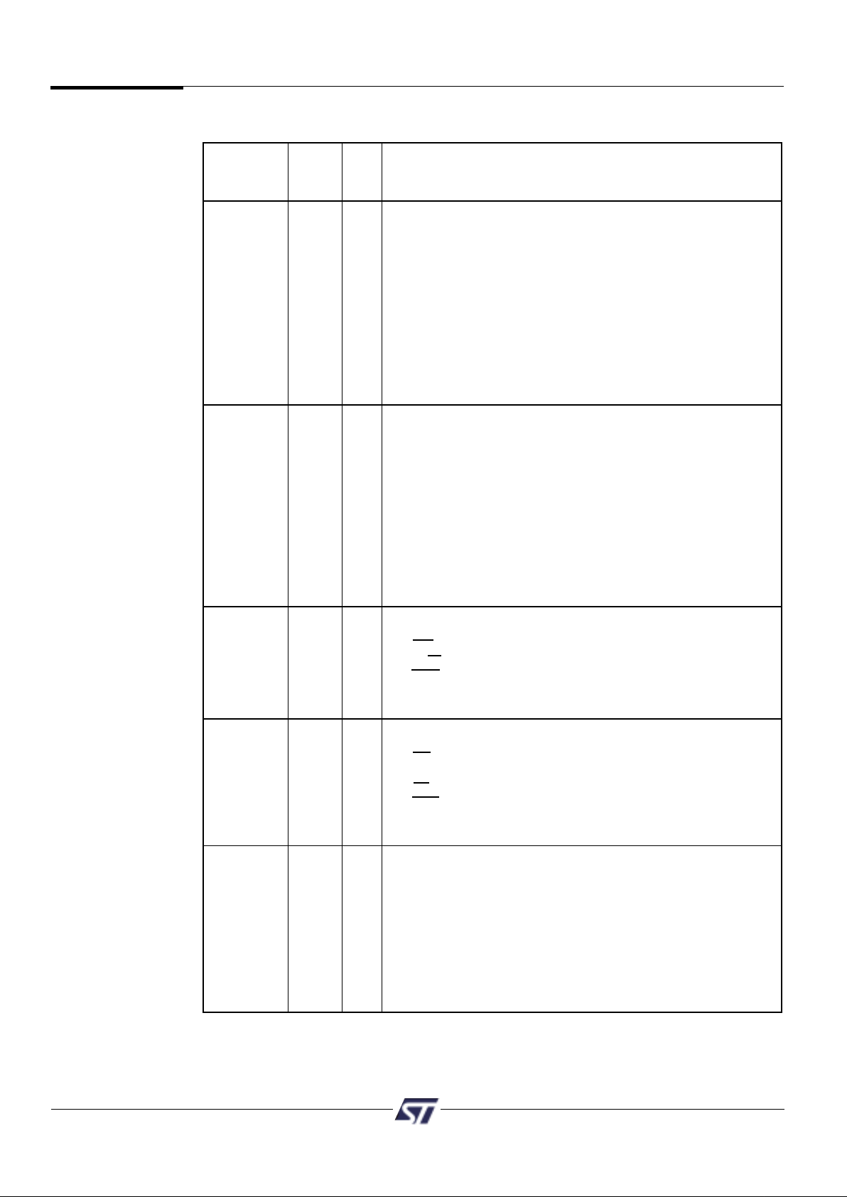
Register Name Port A Port B Port C Port D Port E Port F Port G Other* Description
Data In 00 01 10 11 30 40 41
Reads Port pin as input,
MCU I/O input mode
Control 32 42 43
Selects mode between
MCU I/O or Address Out
Stores data for output
Data Out 04 05 14 15 34 44 45 to Port pins, MCU I/O
output mode
Direction 06 07 16 17 36 46 47
Configures Port pin as
input or output
Configures Port pins as
either CMOS or Open
Drive Select 08 09 18 19 38 48 49 Drain on some pins, while
selecting high slew rate
on other pins.
Flash Protection
C0 Read only – Flash Sector
Protection
Flash Boot
Read only – PSD Security
Protection
C2 and Flash Boot Sector
Protection
PMMR0 B0
Power Management
Register 0
PMMR2 B4
Power Management
Register 2
Page E0 Page Register
Places PSD memory
VM E2
areas in Program and/or
Data space on an
individual basis.
Memory_ID0 F0
Read only – Flash and
SRAM size
Memory_ID1 F1
Read only – Boot type
and size
Table 6. Register Address Offset
Page 15
PSD4000 Series Preliminary Information
12
Bit 7 Bit 6 Bit 5 Bit 4 Bit 3 Bit 2 Bit 1 Bit 0
Port Pin 7 Port Pin 6 Port Pin 5 Port Pin 4 Port Pin 3 Port Pin 2 Port Pin 1 Port Pin 0
Data In Registers – Port A, B, C, D, E, F and G
8.0
Register Bit
Definition
All the registers in the PSD4000 are included here for reference. Detail description of the
registers are found in the Functional Block section of the Data Sheet.
Bit definitions:
Read only registers, read Port pin status when Port is in MCU I/O input Mode.
Bit 7 Bit 6 Bit 5 Bit 4 Bit 3 Bit 2 Bit 1 Bit 0
Port Pin 7 Port Pin 6 Port Pin 5 Port Pin 4 Port Pin 3 Port Pin 2 Port Pin 1 Port Pin 0
Data Out Registers – Port A, B, C, D, E, F and G
Bit definitions:
Latched data for output to Port pin when pin is configured in MCU I/O output mode.
Bit 7 Bit 6 Bit 5 Bit 4 Bit 3 Bit 2 Bit 1 Bit 0
Port Pin 7 Port Pin 6 Port Pin 5 Port Pin 4 Port Pin 3 Port Pin 2 Port Pin 1 Port Pin 0
Direction Registers – Port A, B, C, D, E, F and G
Bit definitions:
Set Register Bit to 0 = configure corresponding Port pin in Input mode (default).
Set Register Bit to 1 = configure corresponding Port pin in Output mode.
Bit 7 Bit 6 Bit 5 Bit 4 Bit 3 Bit 2 Bit 1 Bit 0
Port Pin 7 Port Pin 6 Port Pin 5 Port Pin 4 Port Pin 3 Port Pin 2 Port Pin 1 Port Pin 0
Control Registers – Ports E, F and G
Bit definitions:
Set Register Bit to 0 = configure corresponding Port pin in MCU I/O mode (default).
Set Register Bit to 1 = configure corresponding Port pin in Latched Address Out mode.
Bit 7 Bit 6 Bit 5 Bit 4 Bit 3 Bit 2 Bit 1 Bit 0
Port Pin 7 Port Pin 6 Port Pin 5 Port Pin 4 Port Pin 3 Port Pin 2 Port Pin 1 Port Pin 0
Drive Registers – Ports A, B, D, E, and G
Bit definitions:
Set Register Bit to 0 = configure corresponding Port pin in CMOS output driver (default).
Set Register Bit to 1 = configure corresponding Port pin in Open Drain output driver.
Bit 7 Bit 6 Bit 5 Bit 4 Bit 3 Bit 2 Bit 1 Bit 0
Port Pin 7 Port Pin 6 Port Pin 5 Port Pin 4 Port Pin 3 Port Pin 2 Port Pin 1 Port Pin 0
Drive Registers – Ports C and F
Bit definitions:
Set Register Bit to 0 = configure corresponding Port pin as CMOS output driver (default).
Set Register Bit to 1 = configure corresponding Port pin in Slew Rate mode.
Bit 7 Bit 6 Bit 5 Bit 4 Bit 3 Bit 2 Bit 1 Bit 0
Sec7_Prot Sec6_Prot Sec5_Prot Sec4_Prot Sec3_Prot Sec2_Prot Sec1_Prot Sec0_Prot
Flash Protection Register
Bit definitions: Read Only Register
Sec<i>_Prot 1 = Flash Sector <i> is write protected.
Sec<i>_Prot 0 = Flash Sector <i> is not write protected.
Page 16
Preliminary Information PSD4000 Series
13
8.0
Register Bit
Definition
(cont.)
Bit 7 Bit 6 Bit 5 Bit 4 Bit 3 Bit 2 Bit 1 Bit 0
Security_Bit
***
Sec3_Prot Sec2_Prot Sec1_Prot Sec0_Prot
Flash Boot Protection Register
Bit definitions:
Sec<i>_Prot 1 = Boot Block Sector <i> is write protected.
Sec<i>_Prot 0 = Boot Block Sector <i> is not write protected.
Security_Bit 0 = Security Bit in device has not been set.
1 = Security Bit in device has been set.
Bit 7 Bit 6 Bit 5 Bit 4 Bit 3 Bit 2 Bit 1 Bit 0
Pgr7 Pgr6 Pgr5 Pgr4 Pgr3 Pgr2 Pgr1 Pgr0
Page Register
Bit definitions:
Configure Page input to PLD. Default Pgr[7:0] = 00.
Bit 7 Bit 6 Bit 5 Bit 4 Bit 3 Bit 2 Bit 1 Bit 0
**
PLD PLD PLD
*
APD
*
Mcells clk array-clk Turbo enable
PMMR0 Register
Bit definitions: (default is 0)
Bit 1 0 = Automatic Power Down (APD) is disabled.
1 = Automatic Power Down (APD) is enabled.
Bit 3 0 = PLD Turbo is on.
1 = PLD Turbo is off, saving power.
Bit 4 0 = CLKIN input to the PLD AND array is connected.
Every CLKIN change will power up the PLD when Turbo bit is off.
1 = CLKIN input to PLD AND array is disconnected, saving power.
Bit 5 0 = CLKIN input to the PLD Micro ⇔Cells is connected.
1 = CLKIN input to the PLD Micro ⇔Cells is disconnected, saving power.
*Not used bit should be set to zero.
Bit 7 Bit 6 Bit 5 Bit 4 Bit 3 Bit 2 Bit 1 Bit 0
*
PLD PLD PLD PLD PLD
**
array WRh array Ale array Cntl2 array Cntl1 array Cntl0
PMMR2 Register
Bit definitions (defauld is 0):
Bit 0 0 = Address A[7:0] are connected into the PLD array.
1 = Address A[7:0] are blocked from the PLD array, saving power.
Note: in XA mode, A3-0 come from PF3-0 and A7-4 come from ADIO7-4.
Bit 2 0 = Cntl0 input to the PLD AND array is connected.
1 = Cntl0 input to the PLD AND array is disconnected, saving power.
Bit 3 0 = Cntl1 input to the PLD AND array is connected.
1 = Cntl1 input to the PLD AND array is disconnected, saving power.
Bit 4 0 = Cntl2 input to the PLD AND array is connected.
1 = Cntl2 input to the PLD AND array is disconnected, saving power.
Bit 5 0 = Ale input to the PLD AND array is connected.
1 = Ale input to the PLD AND array is disconnected, saving power.
Bit 6 0 = WRh/DBE input to the PLD AND array is connected.
1 = WRh/DBE input to the PLD AND array is disconnected, saving power.
*Not used bit should be set to zero.
Page 17
PSD4000 Series Preliminary Information
14
8.0
Register Bit
Definition
(cont.)
Bit 7 Bit 6 Bit 5 Bit 4 Bit 3 Bit 2 Bit 1 Bit 0
***
FL_data Boot_data FL_code Boot_code SR_code
VM Register
Bit definitions:
Bit 0 0 = PSEN can’t access SRAM in 80C51XA modes.
1 = PSEN can access SRAM in 80C51XA modes.
Bit 1 0 = PSEN can’t access Boot in 80C51XA modes.
1 = PSEN can access Boot in 80C51XA modes.
Bit 2 0 = PSEN can’t access main Flash in 80C51XA modes.
1 = PSEN can access main Flash in 80C51XA modes.
Bit 3 0 = RD can’t access Boot in 80C51XA modes.
1 = RD can access Boot in 80C51XA modes.
Bit 4 0 = RD can’t access main Flash in 80C51XA modes.
1 = RD can access main Flash in 80C51XA modes.
Note: Upon reset, Bit1-Bit4 are loaded to configurations selected by the user in PSDsoft. Bit 0 is always cleared
by reset. Bit 0 to Bit 4 are active only when the device is configured in Philips 80C51XA mode. Not used
bit should be set to zero.
Bit 7 Bit 6 Bit 5 Bit 4 Bit 3 Bit 2 Bit 1 Bit 0
S_size 3 S_size 2 S_size 1 S_size 0 F_size 3 F_size 2 F_size 1 F_size 0
Memory_ID0 Register
Bit definitions:
F_size[3:0] = 4h, main Flash size is 2M bit.
F_size[3:0] = 5h, main Flash size is 8M bit.
S_size[3:0] = 0h, SRAM size is 0K bit.
S_size[3:0] = 1h, SRAM size is 16K bit.
S_size[3:0] = 3h, SRAM size is 64K bit.
Bit 7 Bit 6 Bit 5 Bit 4 Bit 3 Bit 2 Bit 1 Bit 0
**
B_type 1 B_type 0 B_size 3 B_size 2 B_size 1 B_size 0
Memory_ID1 Register
Bit definitions:
B_size[3:0] = 0h, Boot block size is 0K bit.
B_size[3:0] = 2h, Boot block size is 256K bit.
B_type[1:0] = 0h, Boot block is Flash memory.
*Not used bit should be set to zero.
Page 18
Preliminary Information PSD4000 Series
15
9.0
The
PSD4000
Functional
Blocks
As shown in Figure 1, the PSD4000 consists of six major types of functional blocks:
❏ Memory Blocks
❏ PLD Blocks
❏ Bus Interface
❏ I/O Ports
❏ Power Management Unit
❏ JTAG-ISP Interface
The functions of each block are described in the following sections. Many of the blocks
perform multiple functions, and are user configurable.
9.1 Memory Blocks
The PSD4000 has the following memory blocks:
• The main Flash memory
• Secondary Flash memory
• SRAM.
The memory select signals for these blocks originate from the Decode PLD (DPLD) and
are user-defined in PSDsoft.
Table 7 summarizes which versions of the PSD4000 contain which memory blocks.
Main Flash Secondary Flash
Device Flash Size Sector Size Block Size Sector Size SRAM
PSD4135G2 512KB 64KB 32KB 8KB 8KB
Table 7. Memor y Blocks
9.1.1 Main Flash and Secondary Flash Memory Description
The main Flash memory block is divided evenly into eight sectors. The secondary Flash
memory is divided into four sectors of eight Kbytes each. Each sector of either memory
can be separately protected from program and erase operations.
Flash memory may be erased on a sector-by-sector basis and programmed word-by-word.
Flash sector erasure may be suspended while data is read from other sectors of memory
and then resumed after reading.
During a program or erase of Flash, the status can be output on the Rdy/Bsy pin of Port
PE4. This pin is set up using PSDsoft.
9.1.1.1 Memory Block Selects
The decode PLD in the PSD4000 generates the chip selects for all the internal memory
blocks (refer to the PLD section). Each of the eight Flash memory sectors have a
Flash Select signal (FS0 -FS7) which can contain up to three product terms. Each of the
four Secondary Flash memory sectors have a Select signal (CSBOOT0-3) which can
contain up to three product terms. Having three product terms for each sector select signal
allows a given sector to be mapped in different areas of system memory. When using a
microcontroller (80C51XA) with separate Program and Data space, these flexible select
signals allow dynamic re-mapping of sectors from one space to the other before and after
IAP.
9.1.1.2 The Ready/Busy Pin (PE4)
Pin PE4 can be used to output the Ready/Busy status of the PSD4000. The output on the
pin will be a ‘0’ (Busy) when Flash memory blocks are being written to, or when the Flash
memory block is being erased. The output will be a ‘1’ (Ready) when no write or erase
operation is in progress.
Page 19

PSD4000 Series Preliminary Information
16
9.1.1.3 Memory Operation
The main Flash and secondary Flash memories are addressed through the microcontroller
interface on the PSD4000 device. The microcontroller can access these memories in one
of two ways:
❏ The microcontroller can execute a typical bus write or read operation just as it would
if accessing a RAM or ROM device using standard bus cycles.
❏ The microcontroller can execute a specific instruction that consists of several write
and read operations. This involves writing specific data patterns to special addresses
within the Flash to invoke an embedded algorithm. These instructions are summarized
in Table 8.
Typically, Flash memory can be read by the microcontroller using read operations, just
as it would read a ROM device. However, Flash memory can only be erased and
programmed with specific instructions. For example, the microcontroller cannot write a
single word directly to Flash memory as one would write a word to RAM. To program a
word into Flash memory, the microcontroller must execute a program instruction sequence,
then test the status of the programming event. This status test is achieved by a read
operation or polling the Rdy/Busy pin (PE4).
The Flash memory can also be read by using special instructions to retrieve particular
Flash device information (sector protect status and ID).
9.1.1.3.1 Instructions
An instruction is defined as a sequence of specific operations. Each received byte is
sequentially decoded by the PSD and not executed as a standard write operation. The
instruction is executed when the correct number of bytes are properly received and the
time between two consecutive bytes is shorter than the time-out value. Some instructions
are structured to include read operations after the initial write operations.
The sequencing of any instruction must be followed exactly. Any invalid combination of
instruction bytes or time-out between two consecutive bytes while addressing Flash
memory will reset the device logic into a read array mode (Flash memory reads like a
ROM device).
The PSD4000 main Flash and secondary Flash support these instructions (see Table 8):
❏ Erase memory by chip or sector
❏ Suspend or resume sector erase
❏ Program a word
❏ Reset to read array mode
❏ Read Main Flash Identifier value
❏ Read sector protection status
❏ Bypass Instruction
These instructions are detailed in Table 8. For efficient decoding of the instructions, the
first two bytes of an instruction are the coded cycles and are followed by a command byte
or confirmation byte. The coded cycles consist of writing the data byte AAh to address
XAAAh during the first cycle and data byte 55h to address X554h during the second cycle
(unless the Bypass Instruction feature is used. See 9.1.1.7). Address lines A15-A12 are
don’t care during the instruction write cycles. However, the appropriate sector select signal
(FSi or CSBOOTi) must be selected.
The main Flash and the secondary Flash Block have the same set of instructions (except
Read main Flash ID). The chip selects of the Flash memory will determine which Flash will
receive and execute the instruction. The main Flash is selected if any one of the FS0-7 is
active, and the secondary Flash Block is selected if any one of the CSBOOT0-3 is active.
The
PSD4000
Functional
Blocks
(cont.)
Page 20
Preliminary Information PSD4000 Series
17
FS0-7
Instruction or
(Note 14) CSBOOT0-3 Cycle 1 Cycle 2 Cycle 3 Cycle 4 Cycle5 Cycle 6 Cycle 7
Read (Note 5) 1 “Read”
RA RD
Read Main Flash ID 1 AAh 55h 90h “Read”
(Note 6) @XAAAh @X554h @XAAAh ID
@XX02h
Read Sector Protection 1 AAh 55h 90h “Read”
(Notes 6,8,13) @XAAAh @X554h @XAAAh 00h or 01h
@XX04h
Program a Flash Word 1 AAh 55h A0h PD@PA
@XAAAh @X554h @XAAAh
Erase One Flash Sector 1 AAh 55h 80h AAh 55h 30h 30h
@XAAAh @X554h @XAAAh @XAAAh @X554h @SA @next SA
(Note 7)
Erase Flash Block 1 AAh 55h 80h AAh 55h 10h
(Bulk Erase) @XAAAh @X554h @XAAAh @XAAAh @X554h @XAAAh
Suspend Sector Erase 1 B0h
(Note 11) @xxxh
Resume Sector Erase 1 30h
(Note 12) @xxxh
Reset (Note 6) 1 F0 @any
address
Unlock Bypass 1 AAh 55h 20h
@XAAAh @X554h @XAAAh
Unlock Bypass Program 1 A0h PD@PA
(Note 9) @XXXXh
Unlock Bypass Reset 1 90h 00h
(Note 10) @XXXXh @XXXXh
Table 8. Instructions
X = Don’t Care. “xxxh” address in the above table must be an even address.
RA = Address of the memory location to be read.
RD = Data read from location RA during read operation.
PA = Address of the memory location to be programmed. Addresses are latched on the falling edge of the WR#
(CNTL0) pulse. PA is an even address for PSD in word programming mode.
PD = Data (word) to be programmed at location PA. Data is latched on the rising edge of WR# (CNTL0) pulse.
SA = Address of the sector to be erased or verified. The chip select (FS0-7 or CSBOOT0-3) of the sector to be
erased must be active (high).
NOTES:
1. All bus cycles are write bus cycle except the ones with the “read” label.
2. All values are in hexadecimal.
3. FS0-7 and CSBOOT0-3 are active high and are defined in PSDsoft.
4. Only Address bits A11-A0 are used in Instruction decoding.
5. No unlock or command cycles required when device is in read mode.
6. The Reset command is required to return to the read mode after reading the Flash ID, Sector Protect status
or if DQ5 (DQ13) goes high.
7. Additional sectors to be erased must be entered within 80µs.
8. The data is 00h for an unprotected sector and 01h for a protected sector. In the fourth cycle, the sector chip
select is active and (A1 = 1, A0 = 0).
9. The Unlock Bypass command is required prior to the Unlock Bypass Program command.
10. The Unlock Bypass Reset command is required to return to reading array data when the device is in the
Unlock Bypass mode.
11. The system may read and program functions in non-erasing sectors, read the Flash ID or read the Sector
Protect status, when in the Erase Suspend mode. The erase Suspend command is valid only during a sector
erase operation.
12. The Erase Resume command is valid only during the Erase Suspend mode.
13. The MCU cannot invoke these instructions while executing code from the same Flash memory for which the
instruction is intended. The MCU must fetch, for example, codes from the Secondary Flash memory when
reading the Sector Protection Status of the main Flash.
14. All write bus cycles in an instruction are byte write to even address (XA4Ah or X554h). Flash Programming
bys cycle is writing a word to even address.
The
PSD4000
Functional
Blocks
(cont.)
Page 21

PSD4000 Series Preliminary Information
18
The
PSD4000
Functional
Blocks
(cont.)
9.1.1.4 Power-Up Condition
The PSD4000 internal logic is reset upon power-up to the read array mode. The FSi and
CSBOOTi select signals, along with the write strobe signal, must be in the false state
during power-up for maximum security of the data contents and to remove the possibility of
data being written on the first edge of a write strobe signal. Any write cycle initiation is
locked when VCCis below VLKO.
9.1.1.5 Read
Under typical conditions, the microcontroller may read the Flash, or secondary Flash
memories using read operations just as it would a ROM or RAM device. Alternately, the
microcontoller may use read operations to obtain status information about a program or
erase operation in progress. Lastly, the microcontroller may use instructions to read
special data from these memories. The following sections describe these read functions.
9.1.1.5.1 Read the Contents of Memory
Main Flash and secodary Flash memories are placed in the read array mode after
power-up, chip reset, or a Reset Flash instruction (see Table 8). The microcontroller can
read the memory contents of main Flash or secondary Flash by using read operations any
time the read operation is not part of an instruction sequence.
9.1.1.5.2 Read the Main Flash Memory Identifier
The main Flash memory identifier is read with an instruction composed of 4 operations:
3 specific write operations and a read operation (see Table 8). The PSD4000 main Flash
memory ID is E8h. The Secondary Flash does not support this instruction.
9.1.1.5.3 Read the Flash Memory Sector Protection Status
The Flash memory sector protection status is read with an instruction composed of 4
operations: 3 specific write operations and a read operation (see Table 8). The read
operation will produce 01h if the Flash sector is protected, or 00h if the sector is not
protected.
The sector protection status for all NVM blocks (main Flash or secondary Flash) can also
be read by the microcontroller accessing the Flash Protection and Flash Boot Protection
registers in PSD I/O space. See section 9.1.1.9.1 for register definitions.
9.1.1.5.4 Read the Erase/Program Status Bits
The PSD4000 provides several status bits to be used by the microcontroller to confirm
the completion of an erase or programming instruction of Flash memory. These status bits
minimize the time that the microcontroller spends performing these tasks and are defined
in Table 9. The status byte resides in even location and can be read as many times as
needed. Please note DQ15-8 is even byte for Motorola MCUs with 16 bit data bus.
FSi/
CSBOOTi DQ7 DQ6 DQ5 DQ4 DQ3 DQ2 DQ1 DQ0
Data Toggle Error
Erase
Flash V
IH
Polling Flag Flag
X Time- X X X
out
Table 9. Status Bits
NOTES: 1. X = Not guaranteed value, can be read either 1 or 0.
2. DQ15-DQ0 represent the Data Bus bits, D15-D0.
3. FSi/CSBOOTi are active high.
For Flash memory, the microcontroller can perform a read operation to obtain these status
bits while an erase or program instruction is being executed by the embedded algorithm.
See section 9.1.1.6 for details.
FSi/
CSBOOTi DQ15 DQ14 DQ13 DQ12 DQ11 DQ10 DQ9 DQ8
Data Toggle Error
Erase
Flash V
IH
Polling Flag Flag
X Time- X X X
out
Table 9A. Status Bits for Motorola
Page 22

Preliminary Information PSD4000 Series
19
The
PSD4000
Functional
Blocks
(cont.)
9.1.1.5.5 Data Polling Flag DQ7 (DQ15 for Motorola)
When Erasing or Programming the Flash memory bit DQ7 (DQ15) outputs the complement
of the bit being entered for Programming/Writing on DQ7 (DQ15). Once the Program
instruction or the Write operation is completed, the true logic value is read on DQ7 (DQ15)
(in a Read operation). Flash memory specific features:
❏ Data Polling is effective after the fourth Write pulse (for programming) or after the
sixth Write pulse (for Erase). It must be performed at the address being programmed
or at an address within the Flash sector being erased.
❏ During an Erase instruction, DQ7 (DQ15) outputs a ‘0’. After completion of the
instruction, DQ7 (DQ15) will output the last bit programmed (it is a ‘1’ after erasing).
❏ If the location to be programmed is in a protected Flash sector, the instruction is
ignored.
❏ If all the Flash sectors to be erased are protected, DQ7 (DQ15) will be set to ‘0’ for
about 100 µs, and then return to the previous addressed location. No erasure will be
performed.
9.1.1.5.6 Toggle Flag DQ6 (DQ14 for Motorola)
The PSD4000 offers another way for determining when the Flash memory Program
instruction is completed. During the internal Write operation and when either the FSi or
CSBOOTi is true, the DQ6 (DQ14) will toggle from ‘0’ to ‘1’ and ‘1’ to ‘0’ on subsequent
attempts to read any word of the memory.
When the internal cycle is complete, the toggling will stop and the data read on the
Data Bus is the addressed memory location. The device is now accessible for a new
Read or Write operation. The operation is finished when two successive reads yield the
same output data. Flash memory specific features:
❏ The Toggle bit is effective after the fourth Write pulse (for programming) or after the
sixth Write pulse (for Erase).
❏ If the location to be programmed belongs to a protected Flash sector, the instruction
is ignored.
❏ If all the Flash sectors selected for erasure are protected, DQ6 (DQ14) will toggle to
‘0’ for about 100 µs and then return to the previous addressed location.
9.1.1.5.7 Error Flag DQ5 (DQ14 for Motorola)
During a correct Program or Erase, the Error bit will set to ‘0’. This bit is set to ‘1’ when
there is a failure during Flash programming, Sector erase, or Bulk Erase.
In the case of Flash programming, the Error Bit indicates the attempt to program a Flash
bit(s) from the programmed state (0) to the erased state (1), which is not a valid operation.
The Error bit may also indicate a timeout condition while attempting to program a word.
In case of an error in Flash sector erase or word program, the Flash sector in which the
error occurred or to which the programmed location belongs must no longer be used.
Other Flash sectors may still be used. The Error bit resets after the Reset instruction. A
reset instruction is required after detecting the error bit.
9.1.1.5.8 Erase Time-out Flag DQ3 (DQ11 for Motorola)
The Erase Timer bit reflects the time-out period allowed between two consecutive Sector
Erase instructions. The Erase timer bit is set to ‘0’ after a Sector Erase instruction for a
time period of 100 µs + 20% unless an additional Sector Erase instruction is decoded.
After this time period or when the additional Sector Erase instruction is decoded, DQ3
(DQ11) is set to ‘1’. A reset instruction is required after detecting the erase timer bit.
Page 23

PSD4000 Series Preliminary Information
20
9.1.1.6 Programming Flash Memory
Flash memory must be erased prior to being programmed. The MCU may erase Flash
memory all at once or by-sector. Flash memory sector erases to all logic ones, and its bits
are programmed to logic zeros. Although erasing Flash memory occurs on a sector or chip
basis, programming Flash memory occurs on a word basis.
The PSD4000 main Flash and secondary Flash memories require the MCU to send an
instruction to program a word or perform an erase function (see Table 8).
Once the MCU issues a Flash memory program or erase instruction, it must check for the
status of completion. The embedded algorithms that are invoked inside the PSD4000
support several means to provide status to the MCU. Status may be checked using any of
three methods: Data Polling, Data Toggle, or the Ready/Busy output pin.
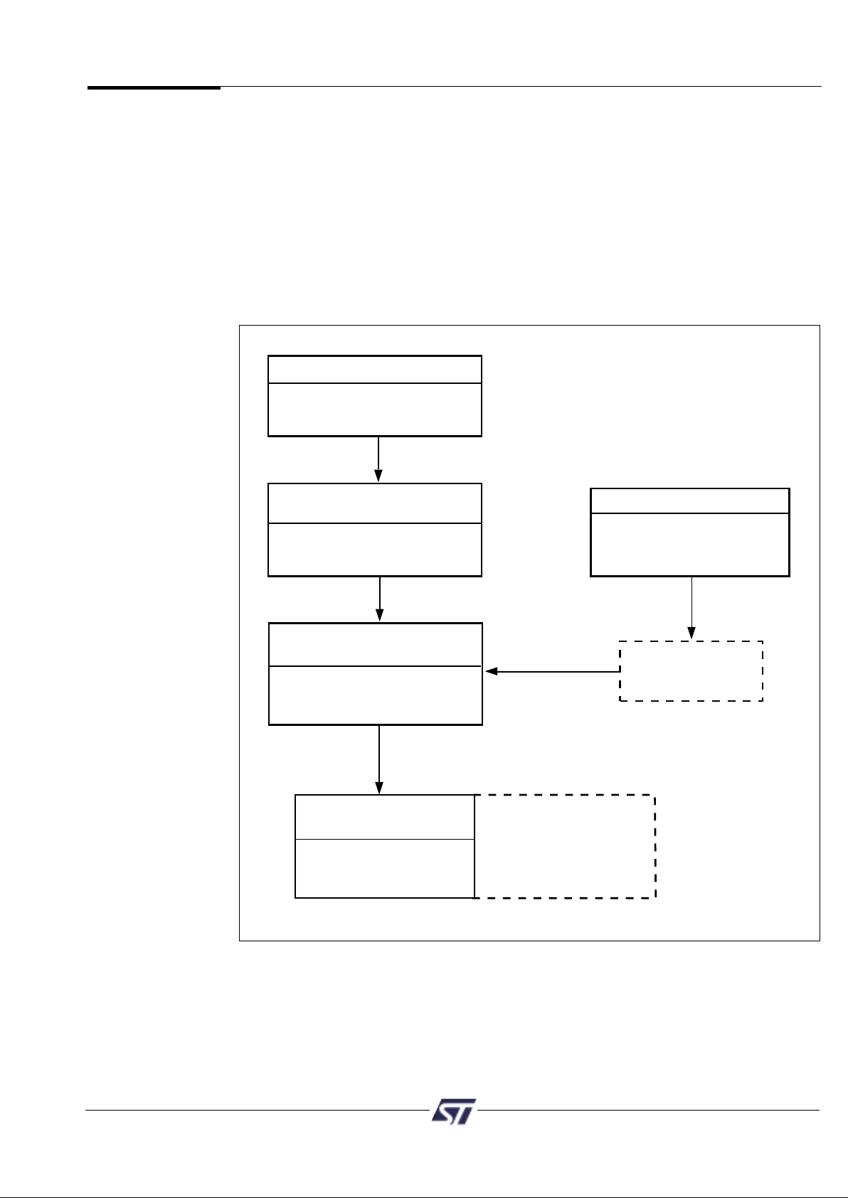
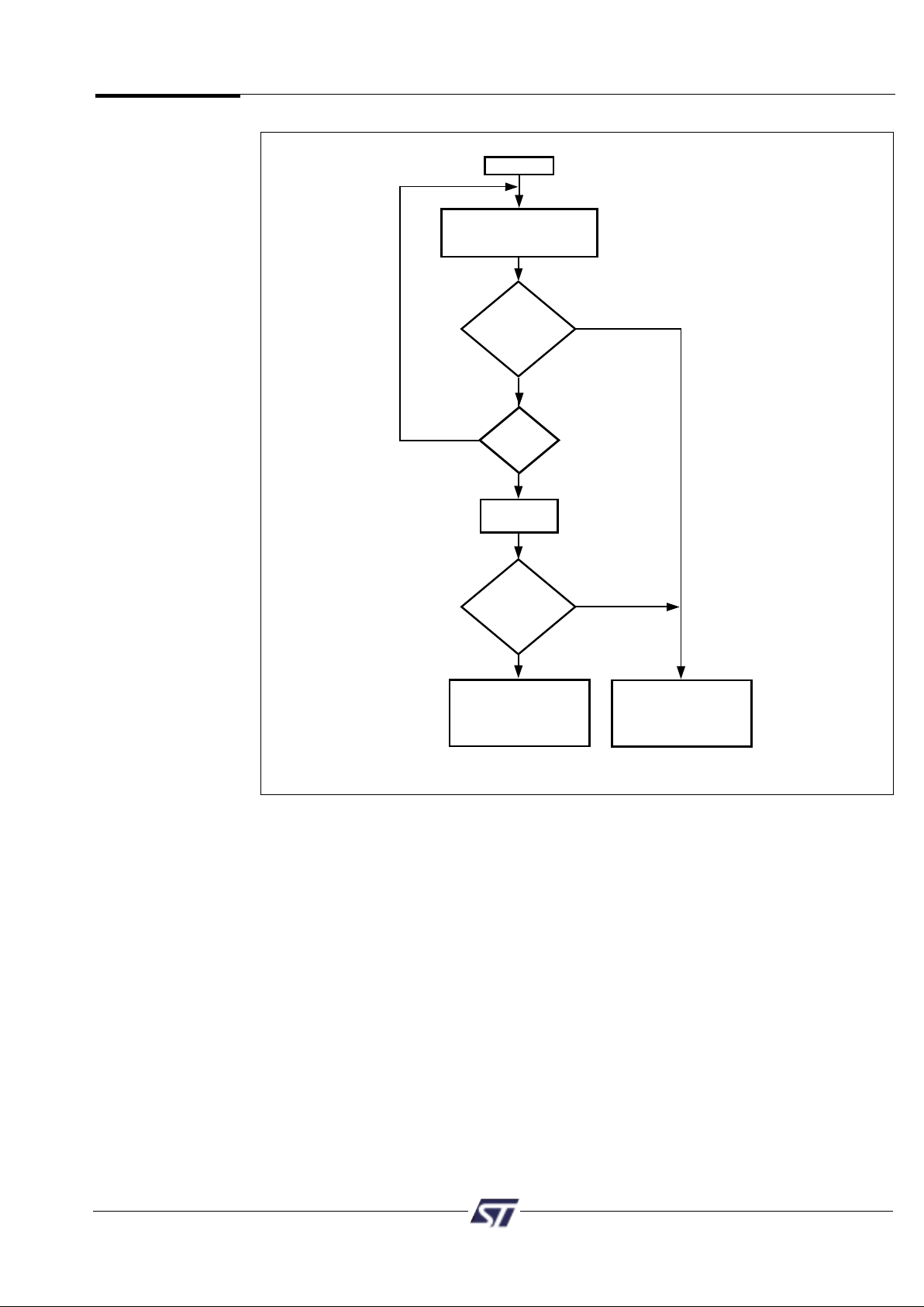
9.1.1.6.1 Data Polling
Polling on DQ7 (DQ15) is a method of checking whether a Program or Erase instruction is
in progress or has completed. Figure 3 shows the Data Polling algorithm.
When the MCU issues a programming instruction, the embedded algorithm within the
PSD4000 begins. The MCU then reads the location of the word to be programmed in Flash
to check status. Data bit DQ7 (DQ15) of this location becomes the compliment of data bit
7of the original data word to be programmed. The MCU continues to poll this location,
comparing DQ7 (DQ15) and monitoring the Error bit on DQ5 (DQ13). When the DQ7
(DQ15) matches data bit 7 of the original data, and the Error bit at DQ5 (DQ13) remains
‘0’, then the embedded algorithm is complete. If the Error bit at DQ5 is ‘1’, the MCU should
test DQ7 (DQ15) again since DQ7 (DQ15) may have changed simultaneously with DQ5
(DQ13) (see Figure 3).
The Error bit at DQ5 (DQ13) will be set if either an internal timeout occurred while the
embedded algorithm attempted to program the location or if the MCU attempted to
program a ‘1’ to a bit that was not erased (not erased is logic ‘0’).
It is suggested (as with all Flash memories) to read the location again after the embedded
programming algorithm has completed to compare the word that was written to Flash with
the word that was intended to be written.
When using the Data Polling method after an erase instruction, Figure 3 still applies.
However, DQ7 (DQ15) will be ‘0’ until the erase operation is complete. A ‘1’ on DQ5
(DQ13) will indicate a timeout failure of the erase operation, a ‘0’ indicates no error.
The MCU can read any location within the sector being erased to get DQ7 (DQ15) and
DQ5 (DQ13) .
PSDsoft generates ANSI C code functions which implement these Data Polling
algorithms.
The
PSD4000
Functional
Blocks
(cont.)
Page 24
Preliminary Information PSD4000 Series
21
Figure 3. Data Polling Flow Chart
START
READ DQ5 & DQ7
(DQ13 & DQ15)
at VALID EVEN ADDRESS
YES
YES
YES
NO
NO
NO
DQ7
(DQ15)
=
DATA7
(DATA15)
DQ5
(DQ13)
=1
READ DQ7
(DQ15)
FAIL
Program/Erase
Operation Failed
Issue Reset Instruction
PASS
Program/Erase
Operation is
Completed
DQ7
(DQ15)
=
DATA7
(DATA15)
The
PSD4000
Functional
Blocks
(cont.)
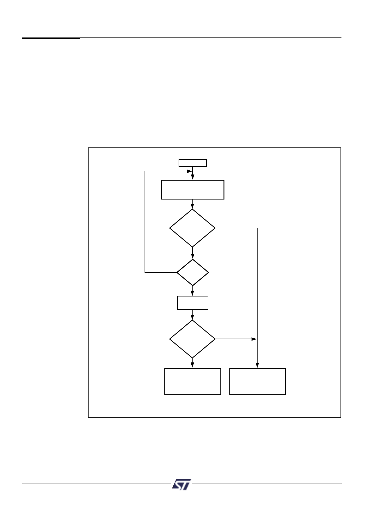
9.1.1.6.2 Data Toggle
Checking the Data Toggle bit on DQ6 (DQ14) is a method of determining whether a
Program or Erase instruction is in progress or has completed. Figure 4 shows the Data
Toggle algorithm.
When the MCU issues a programming instruction, the embedded algorithm within the
PSD4000 begins. The MCU then reads the location to be programmed in Flash to check
status. Data bit DQ6 (DQ14) of this location will toggle each time the MCU reads this
location until the embedded algorithm is complete. The MCU continues to read this
location, checking DQ6 (DQ14) and monitoring the Error bit on DQ5 (DQ13) . When
DQ6 (DQ14) stops toggling (two consecutive reads yield the same value), and the Error bit
on DQ5 (DQ13) remains ‘0’, then the embedded algorithm is complete. If the Error bit on
DQ5 (DQ13) is ‘1’, the MCU should test DQ6 (DQ14) again, since DQ6 (DQ14) may have
changed simultaneously with DQ5 (DQ13) (see Figure 4).
The Error bit at DQ5 (DQ13) will be set if either an internal timeout occurred while the
embedded algorithm attempted to program, or if the MCU attempted to program a ‘1’ to a
bit that was not erased (not erased is logic ‘0’).
Page 25
PSD4000 Series Preliminary Information
22
9.1.1.6.2 Data Toggle (cont.)
It is suggested (as with all Flash memories) to read the location again after the embedded
programming algorithm has completed to compare the word that was written to Flash with
the word that was intended to be written.
When using the Data Toggle method after an erase instructin, Figure 4 still applies. DQ6
(DQ14) will toggle until the erase operation is complete. A ‘1’ on DQ5 (DQ13) will indicate
a timeout failure of the erase operation, a ‘0’ indicates no error. The MCU can read any
even location within the sector being erased to get DQ6 (DQ14) and DQ5 (DQ13) .
PSDsoft generates ANSI C code functions which implement these Data Toggling
algorithms.
The
PSD4000
Functional
Blocks
(cont.)
Figure 4. Data Toggle Flow Chart
START
READ DQ5 & DQ6
(DQ13 & DQ14)
at VALID EVEN ADDRESS
NO
YES
NO
YES
YES
NO
DQ6
(DQ14)
=
TOGGLE
DQ5
(DQ13)
=1
READ DQ6
(DQ14)
FAIL
Program/Erase
Operation Failed
Issue Reset Instruction
PASS
Program/Erase
Operation is
Completed
DQ6
(DQ14)
=
TOGGLE
Page 26

Preliminary Information PSD4000 Series
23
The
PSD4000
Functional
Blocks
(cont.)
9.1.1.7 Unlock Bypass Instruction
The unlock bypass feature allows the system to program words to the flash memories
faster than using the standard program instruction. The unlock bypass instruction is
initiated by first writing two unlock cycles. This is followed by a third write cycle containing
the unlock bypass command, 20h (see Table 8). The flash memory then enters the unlock
bypass mode. A two-cycle Unlock Bypass Program instruction is all that is required to
program in this mode. The first cycle in this instruction contains the unlock bypass
programm command, A0h; the second cycle contains the program address and data.
Additional data is programmed in the same manner. This mode dispenses with the initial
two unlock cycles required in the standard program instruction, resulting in faster total programming time. During the unlock bypass mode, only the Unlock Bypass Program and
Unlock Bypass Reset instructions are valid. To exit the unlock bypass mode, the system
must issue the two-cycle unlock bypass reset instruction. The first cycle must contain the
data 90h; the second cycle the data 00h. Addresses are don’t care for both cycles. The
flash memory then returns to reading array data mode.
9.1.1.8 Erasing Flash Memory
9.1.1.8.1. Flash Bulk Erase Instruction
The Flash Bulk Erase instruction uses six write operations followed by a Read operation of
the status register, as described in Table 8. If any byte of the Bulk Erase instruction is
wrong, the Bulk Erase instruction aborts and the device is reset to the Read Flash memory
status.
During a Bulk Erase, the memory status may be checked by reading status bits DQ5, DQ6,
and DQ7 (DQ13, DQ14, DQ15), as detailed in section 9.1.1.6. The Error bit (returns a ‘1’ if
there has been an Erase Failure (maximum number of erase cycles have been executed).
It is not necessary to program the array with 00h because the PSD4000 will automatically
do this before erasing to 0FFh.
During execution of the Bulk Erase instruction, the Flash memory will not accept any
instructions.
9.1.1.8.2 Flash Sector Erase Instruction
The Sector Erase instruction uses six write operations, as described in Table 8. Additional
Flash Sector Erase confirm commands and Flash sector addresses can be written
subsequently to erase other Flash sectors in parallel, without further coded cycles, if the
additional instruction is transmitted in a shorter time than the timeout period of about
100 µs. The input of a new Sector Erase instruction will restart the time-out period.
The status of the internal timer can be monitored through the level of DQ3 (DQ11) (Erase
time-out bit). If DQ3 (DQ11) is ‘0’, the Sector Erase instruction has been received and the
timeout is counting. If DQ3 (DQ11) is ‘1’, the timeout has expired and the PSD4000 is busy
erasing the Flash sector(s). Before and during Erase timeout, any instruction other than
Erase suspend and Erase Resume will abort the instruction and reset the device to Read
Array mode. It is not necessary to program the Flash sector with 00h as the PSD4000 will
do this automatically before erasing.
During a Sector Erase, the memory status may be checked by reading status bits DQ5,
DQ6, and DQ7 (DQ13, DQ14, DQ15), as detailed in section 9.1.1.6.
During execution of the erase instruction, the Flash block logic accepts only Reset and
Erase Suspend instructions. Erasure of one Flash sector may be suspended, in order to
read data from another Flash sector, and then resumed.
Page 27

PSD4000 Series Preliminary Information
24
The
PSD4000
Functional
Blocks
(cont.)
9.1.1.8.3 Flash Erase Suspend Instruction
When a Flash Sector Erase operation is in progress, the Erase Suspend instruction will
suspend the operation by writing 0B0h to any even address when an appropriate Chip
Select (FSi or CSBOOTi) is true. (See Table 8). This allows reading of data from another
Flash sector after the Erase operation has been suspended. Erase suspend is accepted
only during the Flash Sector Erase instruction execution and defaults to read array
mode. An Erase Suspend instruction executed during an Erase timeout will, in addition to
suspending the erase, terminate the time out.
The Toggle Bit DQ6 stops toggling when the PSD4000 internal logic is suspended. The
toggle Bit status must be monitored at an address within the Flash sector being erased.
The Toggle Bit will stop toggling between 0.1 µs and 15 µs after the Erase Suspend
instruction has been executed. The PSD4000 will then automatically be set to Read Flash
Block Memory Array mode.
If an Erase Suspend instruction was executed, the following rules apply:
• Attempting to read from a Flash sector that was being erased will output invalid data.
• Reading from a Flash sector that was not being erased is valid.
• The Flash memory cannot be programmed, and will only respond to Erase Resume
and Reset instructions (read is an operation and is OK).
• If a Reset instruction is received, data in the Flash sector that was being erased will
be invalid.
9.1.1.8.4 Flash Erase Resume Instruction
If an Erase Suspend instruction was previously executed, the erase operation may be
resumed by this instruction. The Erase Resume instruction consists of writing 030h to any
even address while an appropriate Chip Select (FSi or CSBOOTi) is true. (See Table 8.)
9.1.1.9 Specific Features
9.1.1.9.1 Main Flash and Secondary Flash Sector Protect
Each sector of Main Flash and Secondary Flash memory can be separately protected
against Program and Erase functions. Sector Protection provides additional data
security because it disables all program or erase operations. This mode can be activated
(or deactivated) through the JTAG-ISP Port or a Device Programmer.
Sector protection can be selected for each sector using the PSDsoft program. This will
automatically protect selected sectors when the device is programmed through the JTAG
Port or a Device Programmer. Flash sectors can be unprotected to allow updating of their
contents using the JTAG Port or a Device Programmer. The microcontroller can read (but
cannot change) the sector protection bits.
Any attempt to program or erase a protected Flash sector will be ignored by the device.
The Verify operation will result in a read of the protected data. This allows a guarantee of
the retention of the Protection status.
The sector protection status can either be read by the MCU through the Flash protection
and secondary Flash protection registers (CSIOP), or use the Read Sector Protection
instruction (Table 8).
Page 28

Preliminary Information PSD4000 Series
25
The
PSD4000
Functional
Blocks
(cont.)
Bit 7 Bit 6 Bit 5 Bit 4 Bit 3 Bit 2 Bit 1 Bit 0
Sec7_Prot Sec6_Prot Sec5_Prot Sec4_Prot Sec3_Prot Sec2_Prot Sec1_Prot Sec0_Prot
Flash Protection Register
9.1.1.9.2 Reset Instruction
The Reset instruction consists of one write cycle (see Table 8). It can also be optionally
preceded by the standard two write decoding cycles (writing AAh to AAAh and 55h to
554h).
The Reset instruction must be executed after:
1. Reading the Flash Protection status or Flash ID using the Flash instruction.
2. When an error condition occurs (DQ5 (DQ13) goes high) during a Flash programming
or erase cycle.
The Reset instruction will reset the Flash to normal Read Mode immediately. However, if
there is an error condition (DQ5 (DQ13) goes high), the Flash memory will return to the
Read Mode in 25 µSeconds after the Reset instruction is issued.
The Reset instruction is ignored when it is issued during a Flash programming or Bulk
Erase cycle. The Reset instruction will abort the on going sector erase cycle and return the
Flash memory to normal Read Mode in 25 µSeconds.
9.1.1.9.3 Reset Pin Input
The reset pulse input from the pin will abort any operation in progress and reset the Flash
memory to Read Mode. When the reset occurs during a programming or erase cycle, the
Flash memory will take up to 25 µSeconds to return to Read Mode. It is recommended that
the reset pulse (except power on reset, see Reset Section) be at least 25 µSeconds such
that the Flash memory will always be ready for the MCU to fetch the boot code after reset
is over.
Bit Definitions:
Sec<i>_Prot 1 = Main Flash Sector <i> is write protected.
Sec<i>_Prot 0 = Main Flash Sector <i> is not write protected.
Bit 7 Bit 6 Bit 5 Bit 4 Bit 3 Bit 2 Bit 1 Bit 0
Security_
***
Sec3_Prot Sec2_Prot Sec1_Prot Sec0_Prot
Bit
Flash Boot Protection Register
Bit Definitions:
Sec<i>_Prot 1 = Flash Boot Sector <i> is write protected.
Sec<i>_Prot 0 = Flash Boot Sector <i> is not write protected.
Security_Bit 0 = Security Bit in device has not been set.
1 = Security Bit in device has been set.
Table 10. Sector Protection/Security Bit Definition
*: Not used.
Page 29

PSD4000 Series Preliminary Information
26
The
PSD4000
Functional
Blocks
(cont.)
9.1.2 SRAM
The SRAM is enabled when RS0 —the SRAM chip select output from the DPLD—is high.
RS0 can contain up to three product terms, allowing flexible memory mapping.
The SRAM can be backed up using an external battery. The external battery should be
connected to the Vstby pin (PE6). If you have an external battery connected to the
PSD4000, the contents of the SRAM will be retained in the event of a power loss. The
contents of the SRAM will be retained so long as the battery voltage remains at 2V or
greater. If the supply voltage falls below the battery voltage, an internal power switchover
to the battery occurs.
Pin PE7 can be configured as an output that indicates when power is being drawn from the
external battery. This Vbaton signal will be high with the supply voltage falls below the battery voltage and the battery on PE6 is supplying power to the internal SRAM.
The chip select signal (RS0) for the SRAM, Vstby, and Vbaton are all configured using
PSDsoft.
9.1.3 Memory Select Signals
The main Flash (FSi), secondary Flash (CSBOOTi), and SRAM (RS0) memory select
signals are all outputs of the DPLD. They are defined using PSDsoft. The following rules
apply to the equations for the internal chip select signals:
1. Main Flash memory and secondary Flash memory sector select signals must not be
larger than the physical sector size.
2. Any main Flash memory sector must not be mapped in the same memory space as
another Main Flash sector.
3. A secondary Flash memory sector must not be mapped in the same memory space as
another Flash Boot sector.
4. SRAMand I/O spaces must not overlap.
5. A secondary Flash memory sector may overlap a main Flash memory sector. In case of
overlap, priority will be given to the Flash Boot sector.
6. SRAM, I/O, and Peripheral I/O spaces may overlap any other memory sector. Priority
will be given to the SRAM, and I/O.
Example
FS0 is valid when the address is in the range of 8000h to BFFFh, CSBOOT0 is valid from
8000h to 9FFFh, and RS0 is valid from 8000h to 87FFh. Any address in the range of RS0
will always access the SRAM. Any address in the range of CSBOOT0 greater than 87FFh
(and less than 9FFFh) will automatically address Boot memory segment 0. Any address
greater than 9FFFh will access the Flash memory segment 0. You can see that half of the
Flash memory segment 0 and one-fourth of Boot segment 0 can not be accessed in this
example. Also note that an equation that defined FS1 to anywhere in the range of 8000h to
BFFFh would not be valid.
Figure 5 shows the priority levels for all memory components. Any component on a higher
level can overlap and has priority over any component on a lower level. Components on
the same level must not overlap. Level one has the highest priority and level 3 has the
lowest.
Page 30

Preliminary Information PSD4000 Series
27
The
PSD4000
Functional
Blocks
(cont.)
Level 1
SRAM, I/O
Level 2
Secondary Flash Memory
Highest Priority
Lowest Priority
Level 3
Main Flash Memory
Figure 5. Priority Level of Memory and I/O Components
9.1.3.1. Memory Select Configuration for MCUs with Separate Program and Data Spaces
The 80C51XA and compatible family of microcontrollers, can be configured to have
separate address spaces for code memory (selected using PSEN) and data memory
(selected using RD). Any of the memories within the PSD4000 can reside in either space
or both spaces. This is controlled through manipulation of the VM register that resides in
the PSD’s CSIOP space.
The VM register is set using PSDsoft to have an initial value. It can subsequently be
changed by the microcontroller so that memory mapping can be changed on-the-fly.
For example, you may wish to have SRAM and main Flash in Data Space at boot, and
secondary Flash memory in Program Space at boot, and later swap main and secondary
Flash memory. This is easily done with the VM register by using PSDsoft to configure it for
boot up and having the microcontroller change it when desired.
Table 11 describes the VM Register.
Bit 7 Bit 6* Bit 5* Bit 4 Bit 3 Bit 2 Bit 1 Bit 0
PIO_EN FL_Data Boot_Data FL_Code Boot_Code SRAM_Code
0 = disable
**
0 = RD 0 = RD 0 = PSEN 0 = PSEN 0 = PSEN
PIO mode can’t can’t can’t can’t can’t
access access access access access
Flash Boot Flash Flash Boot Flash SRAM
1= enable
**
1 = RD 1 = RD 1 = PSEN 1 = PSEN 1 = PSEN
PIO mode access access access access access
Flash Boot Flash Flash Boot Flash SRAM
Table 11. VM Register
NOTE: Bits 6-5 are not used.
Page 31

The
PSD4000
Functional
Blocks
(cont.)
MAIN
FLASH
DPLD
FLASH
BOOT
BLOCK
SRAM
RS0
CSBOOT0-3
FS0-7
CS CSCS
OE OE
RD
PSEN
OE
Figure 6. 80C51XA Memory Modes – Separate Space Mode
MAIN
FLASH
DPLD
FLASH
BOOT
BLOCK
SRAM
RS0
CSBOOT0-3
FS0-7
RD
CS CSCS
RD
OE OE
VM REG BIT 2
PSEN
VM REG BIT 0
VM REG BIT 1
VM REG BIT 3
VM REG BIT 4
OE
Figure 7. 80C51XA Memory Mode – Combined Space Mode
9.1.3.2 Configuration Modes for MCUs with Separate Program and Data Spaces
9.1.3.2.1 Separate Space Modes
Code memory space is separated from data memory space. For example, the PSEN
signal is used to access the program code from the main Flash Memory, while the RD
signal is used to access data from the secondary Flash memory, SRAM and I/O Ports.
This configuration requires the VM register to be set to 0Ch.
9.1.3.2.2 . Combined Space Modes
The program and data memory spaces are combined into one space that allows the main
Flash Memory, secondary Flash memory, and SRAM to be accessed by either PSEN or
RD. For example, to configure the main Flash memory in combined space mode, bits 2
and 4 of the VM register are set to “1”.
9.1.3.3 80C51XA Memory Map Example
See Application Notes for examples.
PSD4000 Series Preliminary Information
28
Page 32

Preliminary Information PSD4000 Series
29
RESET
DATA BUS
R/W
D0 Q0
Q1
Q2
Q3
Q4
Q5
Q6
Q7
D1
D2
D3
D4
D5
D6
D7
PAGE
REGISTER
PGR0
PGR1
PGR2
PGR3
DPLD
AND
GPLD
INTERNAL
SELECTS
AND LOGIC
FLASH
PLD
PGR4
PGR5
PGR6
PGR7
Figure 8. Page Register
The
PSD4000
Functional
Blocks
(cont.)
9.1.4 Page Register
The eight bit Page Register increases the addressing capability of the microcontroller by a
factor of up to 256. The contents of the register can also be read by the microcontroller.
The outputs of the Page Register (PGR0-PGR7) are inputs to the PLD decoder and
can be included in the Flash Memory, secondary Flash memory, and SRAM chip select
equations.
If memory paging is not needed, or if not all 8 page register bits are needed for memory
paging, then these bits may be used in the PLD for general logic. See Application
Notes.
Figure 8 shows the Page Register. The eight flip flops in the register are connected to the
internal data bus. The microcontroller can write to or read from the Page Register. The
Page Register can be accessed at address location CSIOP + E0h.
Page 33

PSD4000 Series Preliminary Information
30
The
PSD4000
Functional
Blocks
(cont.)
9.1.5 Memory ID Registers
The 8-bit read only memory status registers are included in the CSIOP space. The user
can determine the memory configuration of the PSD device by reading the Memory ID0
and Memory ID1 registers. The content of the registers are defined as follow:
Bit 7 Bit 6 Bit 5 Bit 4 Bit 3 Bit 2 Bit 1 Bit 0
S_size 3 S_size 2 S_size 1 S_size 0 F_size 3 F_size 2 F_size 1 F_size 0
Memory_ID0 Register
Main Flash Size
F_size3 F_size2 F_size1 F_size0 (Bit)
0 0 0 0 none
0 0 0 1 256K
0 0 1 0 512K
00111M
01002M
01014M
01108M
Bit Definition
SRAM Size
S_size3 S_size2 S_size1 S_size0 (Bit)
0 0 0 0 none
000116K
001032K
001164K
Bit 7 Bit 6 Bit 5 Bit 4 Bit 3 Bit 2 Bit 1 Bit 0
**
B_type 1 B_type 0 B_size 3 B_size 2 B_size 1 B_size 0
Memory_ID1 Register
*Not used bit should be set to zero.
Boot Block Size
B_size3 B_size2 B_size1 B_size0 (Bit)
0 0 0 0 none
0 0 0 1 128K
0 0 1 0 256K
0 0 1 1 512K
Bit Definition
B_type1 B_type0 Boot Block Type
0 0 Flash
0 1 EEPROM
Page 34

Preliminary Information PSD4000 Series
31
The
PSD4000
Functional
Blocks
(cont.)
9.2 PLDs
The PLDs bring programmable logic functionality to the PSD4000. After specifying the
logic for the PLDs in PSDsoft, the logic is programmed into the device and available upon
power-up.
The PSD4000 contains two PLDs: the Decode PLD (DPLD), and the General Purpose
PLD (GPLD). The PLDs are briefly discussed in the next few paragraphs, and in more
detail in sections 9.2.1 and 9.2.2. Figure 10 shows the configuration of the PLDs.
The DPLD performs address decoding for internal components, such as memory,
registers, and I/O port selects.
The GPLD can be used to generate external chip selects, control signals or logic functions.
The GPLD has 24 outputs that are connected to Port A, B and C.
The AND array is used to form product terms. These product terms are specified using
PSDsoft. An Input Bus consisting of 66 signals is connected to the PLDs. The signals are
shown in Table 12. The complement of the 66 signals are also available as inputs to the
AND array.
Input Source Input Name Number
of Signals
MCU Address Bus A[15:0]* 16
MCU Control Signals CNTL[2:0] 3
Reset RST 1
Power Down PDN 1
Port A Input PA[7-0] 8
Port B Input PB[7-0] 8
Port C Input PC[7-0] 8
Port D Inputs PD[3:0] 4
Port F Inputs PF[7:0] 8
Page Register PGR(7:0) 8
Flash Programming Status Bit Rdy/Bsy 1
Table 12. DPLD and GPLD Inputs
NOTE: The address inputs are A[19:4] in 80C51XA mode.
The Turbo Bit
The PLDs in the PSD4000 can minimize power consumption by switching to standby
when inputs remain unchanged for an extended time of about 70 ns. Setting the Turbo
mode bit to off (Bit 3 of the PMMR0 register) automatically places the PLDs into standby if
no inputs are changing. Turbo-off mode increases propagation delays while reducing
power consumption. Refer to the Power Management Unit section on how to set the Turbo
Bit. Additionally, five bits are available in the PMMR2 register to block MCU control signals
from entering the PLDs. This reduces power consumption and can be used only when
these MCU control signals are not used in PLD logic equations.
Page 35

PSD4000 Series Preliminary Information
32
PLD INPUT BUS
8
CSIOP SELECT
SRAM SELECT
FLASH BOOT MEMORY SELECTS
DECODE PLD
PAGE
REGISTER
GPLD
GENERAL PURPOSE PLD
FLASH MEMORY SELECTS
DATA
BUS
8
PLD OUT
PORT A
PORT B
PORT C
PLD OUT
PLD OUT
PORT A PLD INPUT
PORT B PLD INPUT
PORT C PLD INPUT
PORT D PLD INPUT
PORT F PLD INPUT
4
1
1
8
8
8
8
4
8
8
8
66
66
PORT D
PORT F
Figure 9. PLD Block Diagram
Page 36

Preliminary Information PSD4000 Series
33
The
PSD4000
Functional
Blocks
(cont.)
9.2.1 Decode PLD (DPLD)
The DPLD, shown in Figure 10, is used for decoding the address for internal components.
The DPLD can generate the following decode signals:
• 8 sector selects for the main Flash memory (three product terms each)
• 4 sector selects for the Secondary Flash memory (three product terms each)
• 1 internal SRAM select (three product terms)
• 1 internal CSIOP select (select PSD registers, one product term)
Inputs to the DPLD chip selects may include address inputs, Page Register inputs and
other user defined external inputs from Ports A, B, C, D or F.
9.2.2 General Purpose PLD (GPLD)
The General Purpose PLD implements user defined system combinatorial logic function
or chip selects for external devices. Figure 11 shows how the GPLD is connected to the
I/O Ports. The GPLD has 24 outputs and each are routed to a port pin. The port pin can
also be configured as input to the GPLD. When it is not used as GPLD output or input, the
pin can be configured to perform other I/O functions.
All GPLD outputs are identical except in the number of available product terms (PTs) for
logic implementation. Select the pin that can best meet the PT requirement of your logic
function or chip select. In general, a PT is consumed for each logic “OR” function that you
specify in PSDsoft. However, certain logic functions can consume more than one PT even
if no logic “OR” is specified (such as specifying an address range with boundaries of high
granularity).
Table 13 shows the number of “native” PTs for each GPLD output pin. A native PT means
that a particular PT is dedicated to an output pin. For example, Table 13 shows that PSD
Port A pin PA0 has 3 native product terms. This means a guaranteed minimum of 3 PTs is
available to implement logic for that pin.
PSD silicon and PSDsoft can include additional PTs beyong the native PTs to implement
logic. This is a transparent operation that occurs as needed through PT expansion
(internal feedback) or PT allocation (internal borrowing). You may notice in the fitter report
generated by PSDsoft that for a given GPLD output pin, more PTs were used to implement
logic than the number of native PTs available for that pin. This is because PSDsoft has
called on unused PTs from other GPLD output pins to make your logic design fit (PT
allocation or PT expansion). For optimum results, choose a GPLD output pin with a large
number of native PTs for complicated logic.
GPLD Output on Port Pin Number of Native
Product Terms
Port A, pins PA0-3 3
Port A, pins PA4-7 9
Port B, pins PB0-3 4
Port B, pins PB4-7 7
Port C, pins PC0-7 1
Table 13. GPLD Product Term Availability
Page 37

PSD4000 Series Preliminary Information
34
(INPUTS)
(32)
(16)
(1)
PDN (APD OUTPUT)
I/O PORTS (PORT A,B,C,F)
(8)
PGR0 -PGR7
A[15:0
]
*
(4)
(3)
PD[3:0] (ALE,CLKIN,CSI)
CNTRL[2:0
] (
READ/WRITE CONTROL SIGNALS)
(1)
(1)
RESET
RD_BSY
RS0
CSIOP
8 FLASH MEMORY
SECTOR SELECTS
4 SECONDARY
FLASH MEMORY
SECTOR SELECTS
SRAM SELECT
I/O DECODER
SELECT
CSBOOT 0
CSBOOT 1
CSBOOT 2
CSBOOT 3
FS0
FS7
3
3
3
3
3
3
3
3
3
3
3
3
3
Figure 10. DPLD Logic Array
*NOTES: 1. The address inputs are A[19:4] in 80C51XA mode.
2. Additional address lines can be brought into PSD via Port A, B, C, C or F.
Page 38

Preliminary Information PSD4000 Series
35
PRODUCT TERM
PIN PA0-3 HAS 3 NATIVE PTs
PIN PA4-7 HAS 9 NATIVE PTs
POLARITY
SELECT
OTHER I/O
FUNCTION
OTHER I/O
FUNCTION
OTHER I/O
FUNCTION
GENERAL PURPOSE PLD (GPLD) I/O PORT
PLD INPUT BUS
MUX
PLD INPUT
PLD INPUT
PLD INPUT
AND ARRAY
PORT A
PRODUCT TERM
PIN PB0-3 HAS 4 NATIVE PTs
PIN PB4-7 HAS 7 NATIVE PTs
POLARITY
SELECT
PLD OUTPUT
PLD OUTPUT
MUX
AND ARRAY
PORT B
PRODUCT TERM
PIN PC0-7 HAS 1 NATIVE PT
POLARITY
SELECT
PLD OUTPUT
MUX
AND ARRAY
PORT C
*
*
*
Figure 11. The Micro⇔Cell and I/O Port
Page 39

MCU CNTL0 CNTL1 CNTL2 PD3 PD0** ADIO0 PF3-PF0
68302, 68306 R/W LDS UDS
*
AS –
*
MMC2001
68330, 68331
R/W DS SIZ0
*
AS A0
*
68332, 68340
68LC302, WEL OE WEH AS –
*
MMC2001
68HC16 R/W DS SIZ0
*
AS A0
*
68HC912 R/W E LSTRB DBE E A0
*
68HC812*** R/W E LSTRB
**
A0
*
80196 WR RD BHE
*
ALE A0
*
80196SP WRL RD
*
WRH ALE A0
*
80186 WR RD BHE
*
ALE A0
*
80C161
80C164-80C167
WR RD BHE * ALE A0 *
80C51XA WRL RD PSEN WRH ALE A4/D0 A3-A1
H8/3044 WRL RD
*
WRH AS A0 –
M37702M2 R/W E BHE
*
ALE A0
*
PSD4000 Series Preliminary Information
36
The
PSD4000
Functional
Blocks
(cont.)
9.3 Microcontroller Bus Interface
The “no-glue logic” PSD4000 Microcontroller Bus Interface can be directly connected to
most popular microcontrollers and their control signals. Key 16-bit microcontrollers with
their bus types and control signals are shown in Table 14. The MCU interface type is
specified using the PSDsoft.
Table 14. Microcontrollers and their Control Signals
***Unused CNTL2 pin can be configured as GPLD input. Other unused pins (PD3-0, PF3-0) can be
***configured for other I/O functions.
***ALE/AS input is optional for microcontrollers with a non-multiplexed bus.
***This configuration is for 68C812A4_EC at 5MHz, 3V only.
9.3.1. PSD4000 Interface to a Multiplexed Bus
Figure 16 shows an example of a system using a microcontroller with a 16-bit multiplexed
bus and a PSD4000. The ADIO port on the PSD4000 is connected directly to the
microcontroller address/data bus. ALE latches the address lines internally. Latched
addresses can be brought out to Port E, F or G. The PSD4000 drives the ADIO data bus
only when one of its internal resources is accessed and the RD input is active. Should the
system address bus exceed sixteen bits, Ports A, B, C, or F may be used as additional
address inputs.
9.3.2. PSD4000 Interface to a Non-Multiplexed Bus
Figure 17 shows an example of a system using a microcontroller with a 16-bit
non-multiplexed bus and a PSD4000. The address bus is connected to the ADIO Port, and
the data bus is connected to Port F and G. Port F and G are in tri-state mode when the
PSD4000 is not accessed by the microcontroller. Should the system address bus exceed
sixteen bits, Ports A, B or C may be used for additional address inputs.
Page 40

Preliminary Information PSD4000 Series
37
The
PSD4000
Functional
Blocks
(cont.)
MICRO-
CONTROLLER
WR
RD
BHE
ALE
RESET
AD[7:0
]
AD[15:8
]
A[15:8
]
A[7:0
]
ADIO
PORT
PORT
F
PORT
G
PORT
A,B, or
C
WR (CNTRL0
)
RD (CNTRL1
)
BHE (CNTRL2
)
RST
ALE (PD0
)
PORT D
(
OPTIONAL
)
A[23:16
]
(
OPTIONAL
)
(
OPTIONAL
)
PSD4135G2
Figure 12. An Example of a Typical 16-Bit Multiplexed Bus Interface
MICRO-
CONTROLLER
WR
RD
BHE
ALE
RESET
D[15:0
]
A[15:0
]
A[23:16
]
D[7:0
]
ADIO
PORT
PORT
F
PORT
G
PORT
A,B or
C
WR (CNTRL0
)
RD (CNTRL1
)
BHE (CNTRL2
)
RST
ALE (PD0
)
PORT D
(OPTIONAL)
D[15:8
]
(OPTIONAL)
PSD4135G2
Figure 13. An Example of a Typical 16-Bit Non-Multiplexed Bus Interface
Page 41

PSD4000 Series Preliminary Information
38
9.3.3 Data Byte Enable Reference
Microcontrollers have different data byte orientations. The following tables show how the
PSD4135G2 interprets byte/word operation in different bus write configurations. Even-byte
refers to locations with address A0 equal to zero and odd byte as locations with A0 equal
to one.
9.3.4 Microcontroller Interface Examples
Figures 14 through 17 show examples of the basic connections between the PSD4135G2
and some popular microcontrollers. The PSD4135G2 Control input pins are labeled as the
microcontroller function for which they are configured. The MCU interface is specified using
PSDsoft. The PE6 pin should be grounded if Vstby is not used.
9.3.4.1 80C196 and 80C186
In Figure 14, the Intel 80C196 microcontroller, which has a multiplexed sixteen-bit bus, is
shown connected to a PSD4135G2. The WR and RD signals are connected to the
CNTL0-1 pins. The BHE signal is used for high data byte selection. If BHE is not used, the
PSD can be configured to receive the WRL and WRH from the MCU. Higher address
inputs (A16-A19) can be routed to Port A, B or C as inputs to the PLD.
The AMD 80186 family has the same bus connection to the PSD as the 80C196.
BHE A0 D15-D8 D7-D0
0 0 Odd Byte Even Byte
0 1 Odd Byte –
1 0 – Even Byte
Table 15. 16-Bit Data Bus with BHE
The
PSD4000
Functional
Blocks
(cont.)
WRH WRL D15-D8 D7-D0
0 0 Odd Byte Even Byte
0 1 Odd Byte –
1 0 – Even Byte
Table 16. 16-Bit Data Bus with WRH and WRL
SIZ0 A0 D15-D8 D7-D0
0 0 Even Byte Odd Byte
1 0 Even Byte –
1 1 – Odd Byte
Table 17. 16-Bit Data Bus with SIZ0, A0 (Motorola MCU)
LDS UDS D15-D8 D7-D0
0 0 Even Byte Odd Byte
1 0 Even Byte –
0 1 – Odd Byte
Table 18. 16-Bit Data Bus with UDS, LDS (Motorola MCU)
Page 42

Preliminary Information PSD4000 Series
39
The
PSD4000
Functional
Blocks
(cont.)
9.3.4.2 MC683XX and 68HC16
Figure 15 shows a Motorola MC68331 with non-multiplexed sixteen-bit data bus and 24-bit
address bus. The data bus from the MC68331 is connected to Port F (D0-7) and Port G
(D8-D15). The SIZ0 and A0 inputs determine the high/low byte selection. The R/W, DS
and SIZ0 are connected to the CNTL0-2 pins.
The 68HC16 and other members of the 683XX family have the same connection as the
68331 shown in Figure 15.
9.3.4.3 80C51XA
The Philips 80C51XA microcontroller has a 16-bit multiplexed bus with burst cycles.
Address bits A[3:1] are not multiplexed while A[19:4] are multiplexed with data bits D[15:0].
The PSD4135G2 supports the 80C51XA burst mode. The WRH signal is connected to the
PD3 and the WRL is connected to CNTL0 pin. The RD and PSEN signal is connected to
CNTL1-2 pins. Figure 15 shows the XA schematic.
The 80C51XA improves bus throughput and performance by issuing Burst cycles to fetch
codes from memory. In Burst cycles, addresses A19-4 are latched internally by the PSD,
while the 80C51XA drives the A3-1 lines to sequentially fetch up to 16 bytes of code. The
PSD access time is then measured from address A3-A1 valid to data in valid. The PSD
bus timing requirement in Burst cycle is identical to the normal bus cycle except the
address set up or hold time with respect to ALE is not required.
9.3.4.4 H8/300
Figure 16 shows a Hitachi H8/2350 with non-multiplexed sixteen-bit data bus and 24-bit
address bus. The H8 data bus is connected to Port F (D0-7) and Port G (D8-15).
The WRL, WRH and RD signals are connected to the CNTL0, PD3 and CNTL1 pins
respectively. The AS connection is optional and is required if the address are to be
latched.
9.3.4.5 MMC2001
The Motorola MCORE MMC2001 microcontroller has a MOD input pin that selects internal
or external boot ROM. The PSD4000 can be configured as the external flash boot ROM or
as extension to the internal ROM.
The MMC2001 has a 16-bit external data bus and 20 address lines with external Chip
Select signals. The Chip Select Control Registers allow the user to customize the bus
interface and timing to fit the individual system requirement. A typical interface configuration to the PSD4000 is shown in Figure 18. The MMC2001’s R/W signal is connected to
the cntl0 pin, while EB0 and EB1 (enable byte0 and byte1) are connected to the cntl1
(UDS) and cntl2 (LDS) pins. The WEN bit in the Chip Select Control Register should set to
1 to terminate the EB[0:1] earlier to provide the write data hold time for the PSD. The WSC
and WWS bits in the Control Register are set to wait states that meet the PSD access time
requirement.
Another option is to configure the EB0 and EB1 as WRL and WRH signals. In this case the
PSD4000 control setting will be: OE, WRL, WRH where OE is the read signal from the
MMC2001.
9.3.4.6 C16X Family
The PSD4000 supports Infineon’s C16X family of microcontrollers (C161-C167) in both the
multiplexed and non-multiplexed bus configuration. In Figure 19 the C167CR is shown
connected to the PSD4000 in a multiplexed bus configuration. The control signals from the
MCU are WR, RD, BHE and ALE and are routed to the corresponding PSD pins.
The C167 has another control signal setting (RD, WRL, WRH, ALE) which is also
supported by the PSD4000.
Page 43

PSD4000 Series Preliminary Information
40
GND
8
RESET
30 49 50 70
PSD4135G2
V
CC
92969
V
CC
V
CC
V
CC
GND GND GND GND
A[19:16]
A[19:16]
AD[15:0]
AD[15:0]
V
CC
80C196NT
A16
A17
A18
A19
P3.0/AD0
P3.1/AD1
P3.2/AD2
P3.3/AD3
P3.4/AD4
P3.5/AD5
P3.6/AD6
P3.7/AD7
P4.0/AD8
P4.1/AD9
P4.2/AD10
P4.3/AD11
P4.4/AD12
P4.5/AD13
P4.6/AD14
P4.7/AD15
EP.0/A16
EP.1/A17
EP.2/A18
EP.3/A19
WR/WRL/P5.2
RD/P5.3
BHE/WRH/P5.5
ALE/ADV/P5.0
RESET
READY/P5.6
EA
BUSWIDTH/P5.7
INST/P5.1
SLPINT/P5.4
302928272625242322212019181716151413121197 8
4
31
2
33103
1
34567
1011121314151617181920
59
60
40
79
80
1
2
39
71727374757677
78
AD0
AD1
AD2
AD3
AD4
AD5
AD6
AD7
AD8
AD9
AD10
AD11
AD12
AD13
AD14
AD15
X1
X2
NMI
P6.0/EPA8
P6.1EPA9
P6.2/T1CLK
P6.3/T1DIR
ACH4/P0.4/PMD.0
ACH5/P0.5/PMD.1
ACH6/P0.6/PMD.2
ACH7/P0.7/PMD.3
P2.0/TX/PVR
P2.1/RXD/PALE
P2.2/EXINT/PROG
P2.3/INTB
P2.4/INTINTOUT
P2.5/HLD
P2.6/HLDA/CPVER
P2.7/CLKOUT/PAC
P6.4/SC0
P6.5/6D0
P6.6/SC1
P6.7/SD1
VREF
VPP
ANGND
P1.7/EPA7
P1.0/EPAQ/T2CLK
P1.1/EPA1
P1.2/EPA2/T2DIR
P1.3/EPA3
P1.4/EPA4
P1.5/EPA5
P1.6/EPA6
67
66
32
5859606144454647363738394041424362635465496485057565554535251
ADIO0
ADIO1
ADIO2
ADIO3
ADIO4
ADIO5
ADIO6
ADIO7
PF0
PF1
PF2
PF3
PF4
PF5
PF6
PF7
PG0
PG1
PG2
PG3
PG4
PG5
PG6
PG7
PA0
PA1
PA2
PA3
PA4
PA5
PA6
PA7
PB0
PB1
PB2
PB3
PB4
PB5
PB6
PB7
PC0
PC1
PC2
PC3
PC4
PC5
PC6
PC7
313233343536373821222324252627285152535455565758616263646566676841424344454647
48
ADIO8
ADI09
ADIO10
ADIO11
ADIO12
ADIO13
ADIO14
ADIO15
CRTL0 (WR)
CNTL1 (RD)
CNTL2 (BHE)
PDO (ALE)
PD1 (CLKIN)
PD2 (CSI)
PD3 (WRH)
RESET
PEO (TMS)
PE1 (TCK/ST)
PE2 (TDI)
PD2 (TDO)
PE4 (TSTAT/RDY)
PE5 (TERR)
PE6 (VSTBY)
PE7 (VBATON)
U3
CRYATAL
RESET
ALE
BHE
RD
WR
A16
A17
A18
A19
Figure 14. Interfacing the PSD4135G2 with an 80C196
Page 44

Preliminary Information PSD4000 Series
41
GND
8
RESET
RESET
30 49 50 70
PSD4135G2
V
CC
92969
V
CC
V
CC
V
CC
GND GND GND GND
D[15:0]
D[15:0]
A[23:0]
A[23:0]
MC68331
(SIZ0)
A0A1A2A3A4A5A6A7A8
A9
A10
A11
A12
A13
A14
A15
A16
A17
A18
A19_CS6
A20_CS7
A21_CS8
A22_CS9
A23_CS10
R_W
DS
SIZ0
AS
RESET
SIZ1
CLKOUT
CSBOOT
BR_CSO
BG_CS1
BGACK_CS2
FCO_CS3
FC1_CS4
FC2_CS5
90202122232425262730313233353637384142
121
122
123
124
125
79
85
111
110
109
108
105
104
103
102
89
88
77767574737271
34567
1011121314151617181920
59
60
40
79
80
1
2
39
71727374757677
78
A0A1A2A3A4A5A6A7A8A9A10
A11
A12
A13
A14
A15
ADIO0
ADIO1
ADIO2
ADIO3
ADIO4
ADIO5
ADIO6
ADIO7
PF0
PF1
PF2
PF3
PF4
PF5
PF6
PF7
PG0
PG1
PG2
PG3
PG4
PG5
PG6
PG7
PA0
PA1
PA2
PA3
PA4
PA5
PA6
PA7
PB0
PB1
PB2
PB3
PB4
PB5
PB6
PB7
PC0
PC1
PC2
PC3
PC4
PC5
PC6
PC7
313233343536373821222324252627285152535455565758616263646566676841424344454647
48
D0D1D2D3D4D5D6D7D8D9D10
D11
D12
D13
D14
D15
A16
A17
A18
A19
ADIO8
ADIO9
ADIO10
ADIO11
ADIO12
ADIO13
ADIO14
ADIO15
CRTL0 (R/W)
CNTL1 (DS)
CNTL2
PD0 (AS)
PD1 (CLKIN)
PD2 (CSI)
PD3
RESET
PE0 (TMS)
PE1 (TCK/ST)
PE2 (TDI)
PD3 (TDO)
PE4 (TSTAT/RDY)
PE5 (TERR)
PE6 (VSTBY)
PE7 (VBATON)
DSACK0
DSACK1
IRQ1
IRQ2
IRQ3
IRQ4
IRQ5
IRQ6
IRQ7
100
99989794939291
D0D1D2D3D4D5D6
D7
D8D9D10
D11
D12
D13
D14
D15
D0D1D2D3D4D5D6
D7
D8D9D10
D11
D12
D13
D14
D15
81
82
68
80
66
112
113
114
115
118
119
120
R/W
DS
AS
SIZ0
RESET
A16
A17
A18
A19
A20
A21
A22
A23
Figure 15. Interfacing the PSD4135G2 with an MC68331
Page 45

PSD4000 Series Preliminary Information
42
GND
8
RESET
RESET
30 49 50 70
PSD4135G2
XA-G3
V
CC
9
A1A2A3
29 69
V
CC
V
CC
V
CC
GND GND GND GND
D[15:0]
D[15:0]
A[3:1]
A[3:1]
V
CC
A4D0
A5D1
A6D2
A7D3
A8D4
A9D5
A10D6
A11D7
A12D8
A13D9
A14D10
A15D11
A16D12
A17D13
A18D14
A19D15
A3A2A1
A0/WRH
WRL
RD
PSEN
ALE
43424140393837362425262728293031543
2
18
19
32
33
21
20
11
13
679
8
10
10
14
15
35
17
34567
1011121314151617181920
59
60
40
79
80
1
2
39
71727374757677
78
A4D0
A5D1
A6D2
A7D3
A8D4
A9D5
A10D6
A11D7
A12D8
A13D9
A14D10
A15D11
A16D12
A17D13
A18D14
A19D15
XTAL1
XTAL2
RXD0
TXD0
RXD1
TXD1
T2EXT2T0
RST
INT0
INT1
EA/WAIT
BUSW
ADIO0
ADIO1
ADIO2
ADIO3
ADIO4
ADIO5
ADIO6
ADIO7
PF0
PF1
PF2
PF3
PF4
PF5
PF6
PF7
PG0
PG1
PG2
PG3
PG4
PG5
PG6
PG7
PA0
PA1
PA2
PA3
PA4
PA5
PA6
PA7
PB0
PB1
PB2
PB3
PB4
PB5
PB6
PB7
PC0
PC1
PC2
PC3
PC4
PC5
PC6
PC7
313233343536373821222324252627285152535455565758616263646566676841424344454647
48
ADIO8
ADI09
ADIO10
ADIO11
ADIO12
ADIO13
ADIO14
ADIO15
CRTL0 (WR)
CNTL1 (RD)
CNTL2
PD0 (ALE)
PD1 (CLKIN)
PD2 (CSI)
PD3 (WRH)
RESET
PEO (TMS)
PE1 (TCK/ST)
PE2 (TDI)
PD3 (TDO)
PE4 (TSTAT/RDY)
PE5 (TERR)
PE6 (VSTBY)
PE7 (VBATON)
CRYATAL
WRL
RD
PSEN
ALE
A3A2A1
WRH
Figure 16. Interfacing the PSD4135G2 with a 80C51XA-G3
Page 46

Preliminary Information PSD4000 Series
43
GND
8
RESET
RESET
30 49 50 70
PSD4135G2
V
CC
92969
V
CC
V
CC
V
CC
GND GND GND GND
D[15:0]
D[15:0]
A[23:0]
A[23:0]
H85/2350
PC0/A0
PC1/A1
PC2/A2
PC3/A3
PC4/A4
PC5/A5
PC6/A6
PC7/A7
PB0/A8
PB1/A9
PB2/A10
PB3/A11
PB4/A12
PB5/A13
PB6/A14
PB7/A15
PA0/A16
PA1/A17
PA2/A18
PB3/A19
PA4/A20/IRQ4
PA5/A21/IRQ5
PA6/A22/IRQ6
PA7/A23/1RQ7
LWR
RD
23457891011121314161718192021222325262728 85
83
84 73
72
75
112
111
110
109
108
107
106
1059596979899100
101
102
92
116
117
118
119
120
34353637394041
42
2930313255535756545890899188878674717069686766656460616263
113
114
115
80
3456710111213141516171819
20
596040798012
397172737475767778
A0A1A2A3A4A5A6A7A8A9A10
A11
A12
A13
A14
A15
PE0/D0
PE0/D1
PE0/D2
PE0/D3
PE0/D4
PE0/D5
PE0/D6
PE0/D7
PD0/D8
PD1/D9
PD2/D10
PD3/D11
PD4/D12
PD5/D13
PD6/D14
PD7/D15
ADIO0
ADIO1
ADIO2
ADIO3
ADIO4
ADIO5
ADIO6
ADIO7
PF0
PF1
PF2
PF3
PF4
PF5
PF6
PF7
PG0
PG1
PG2
PG3
PG4
PG5
PG6
PG7
PA0
PA1
PA2
PA3
PA4
PA5
PA6
PA7
PB0
PB1
PB2
PB3
PB4
PB5
PB6
PB7
PC0
PC1
PC2
PC3
PC4
PC5
PC6
PC7
313233343536373821222324252627285152535455565758616263646566676841424344454647
48
D0D1D2D3D4D5D6D7D8D9D10
D11
D12
D13
D14
D15
A16
A17
A18
A19
ADIO8
ADIO9
ADIO10
ADIO11
ADIO12
ADIO13
ADIO14
ADIO15
CRTL0 (WRL)
CNTL1 (RD)
CNTL2
PDO (AS)
PD1 (CLKIN)
PD2 (CSI)
PD3 (WRH)
RESET
PE0 (TMS)
PE1 (TCK/ST)
PE2 (TDI)
PD3 (TDO)
PE4 (TSTAT/RDY)
PE5 (TERR)
PE6 (VSTBY)
PE7 (VBATON)
CS7/IRQ3
CS6/IRQ2
IRQ1
IRQ0
RXD0
TXD0
SCK0
PXD1
TXD1
SCK1
RXD2
TXD2
SCK2
PF0/BREQ
PF1/BACK
PF2/LCAS/WAIT/B
NMI
PO0/TIOCA3
PO1/TIOCB3
PO2/TIOC3/TMRI
PO3/TIOCD3/TMCI
PO4/TIOCA4/TMRI
PO5/TIOB4/TMRC
PO6/TI0C5/TMRO
PO7/TIOCB5/TMRO
DREQ/CS4
TEND0/CS5
DREQ1
TEND1
MOD0
MOD1
MOD2
PF0/PHI0
AS
HWR
RESET
WDTOVF
STBY
PO8/TIOCA0/DACK
PO9/TIOCB0/DACK
PO10/TIOCC0/TCL
PO11/TIOCD0/TCL
PO12/TIOCA1
PO13/TIOCB1/TCL
PO14/TIOCA2
PO15/TIOCB2/TCL
AN0
AN1
AN2
AN3
AN4
AN5
AN6/DA0
AN7/DA1
ADTRG
PG0/CAS/OE
PG1/CS3
PG2/CS2
PG3/CS1
PG4/CS0
EXTAL
XTAL
U3
CRYATAL
43444546484950
51
82
WRL
D0D1D2D3D4D5D6
D7
D8D9D10
D11
D12
D13
D14
D15
78
77
A16
A17
A18
A19
A20
A21
A22
A23
RD
AS
WRH
RESET
Figure 17. Interfacing a PSD4135G2 with a H83/2350
Page 47

PSD4000 Series Preliminary Information
44
GND
8
RESET
RESET
30 49 50 70
U2
V
CC
92969
V
CC
V
CC
V
CC
GND GND GND GND
D[15:0]
D[15:0]
A[21:0]
A[21:0]
UI
PSD4135G2
MMC2001
ADDR0
ADDR1
ADDR2
ADDR3
ADDR4
ADDR5
ADDR6
ADDR7
ADDR8
ADDR9
ADDR10
ADDR11
ADDR12
ADDR13
ADDR14
ADDR15
ADDR16
ADDR17
ADDR18
ADDR19
ADDR20
ADDR21
42434445505152535456576061626364656669707172 73
74
82
81
75
76
79
80
113
114
115
116
117
118
119
120
103
104
105
106
107
108
109
1129291907877686758593637262719205521124647
48
22232425282930
31
129
130
131
132
121
124
125
126
128
139
140
141
142
143
144
9394959697
100
101
102
84
83
858687
88
89
12364
5
7
8
9 1011
17
18
13
16
34567
1011121314151617181920
59
60
40
79
80
1
2
39
71727374757677
78
A0A1A2A3A4A5A6A7A8A9A10
A11
A12
A13
A14
A15
EXOSC
XSOC
DATA0
DATA1
DATA2
DATA3
DATA4
DATA5
DATA6
DATA7
DATA8
DATA9
DATA10
DATA11
DATA12
DATA13
DATA14
DATA15
TXD1/SIZ0
RXD1/SIZ1
TXD0/PSTAT0
RXD0/PSTAT1
RTS0/PSTAT2
CTS0/PSTAT3
SPI_MISO
SPI_MISI
SPI_EN
SPI_CLK
SPI_GP
PWM0
PWM1
PWM2
PWM3
PWM4
PWM5
INT7
INT6
INT5
INT4
INT3
INT2
INT1
INT0DETDO
TMS
TD1
TCK
TRST
TESTIFGPS_OUT
FVDD
FGND
CLKOUT
CLKIN
RSTOUT
RSTIN
LVRSTIN
VBATT
VSTBY MOD
XVDD
XGND
XGND
ADIO0
ADIO1
ADIO2
ADIO3
ADIO4
ADIO5
ADIO6
ADIO7
PF0
PF1
PF2
PF3
PF4
PF5
PF6
PF7
PG0
PG1
PG2
PG3
PG4
PG5
PG6
PG7
PA0
PA1
PA2
PA3
PA4
PA5
PA6
PA7
PB0
PB1
PB2
PB3
PB4
PB5
PB6
PB7
PC0
PC1
PC2
PC3
PC4
PC5
PC6
PC7
313233343536373821222324252627285152535455565758616263646566676841424344454647
48
D0D1D2D3D4D5D6D7D8D9D10
D11
D12
D13
D14
D15
A16
*
A17
A18
A19
ADIO8
ADIO9
ADIO10
ADIO11
ADIO12
ADIO13
ADIO14
ADIO15
CRTL0 (R/W)
CNTL1 (LDS)
CNTL2 (UDS)
PD0 (AS)
PD1 (CLKIN)
PD2 (CSI)
PD3
RESET
PE0 (TMS)
PE1 (TCK/ST)
PE2 (TDI)
PE3 (TDO)
PE4 (TSTAT/RDY)
PE5 (TERR)
PE6 (VSTBY)
PE7 (VBATON)
R/W
OE
EB1
EB0
CS0
CS1
CS2
CS3
ROW7
ROW6
ROW5
ROW4
ROW3
ROW2
ROW1
ROW0
COL7
COL6
COL5
COL4
COL3
COL2
COL1
COL0
QVCC
QVCCH
QGND
CVDD
CGND
AVDD2
AGND2
AVDD1
AGND1
DVDD1
DGMD1
DVDD0
DGND0
QVCC
QVCCH
QVCCH
QGND
NOT USED
AGND0
QGND
QVCC
U3
CRYATAL
32333435383940
41
135
136
R/W
D0D1D2D3D4D5D6
D7
D8D9D10
D11
D12
D13
D14
D15
14
15
A16
A17
A18
A19
A20
A21
LDS
UDS
CSO
*
RESET
GVDD0
GGND0
GVDD1
GGND1
HVDD
HGND
QVCCH
QVCC
QGND
JVDD
JGND
99
98
110
111
122
123
127
133
134
137
138
Figure 18. Interfacing a PSD4135G2 with a MMC2001
Page 48

Preliminary Information PSD4000 Series
45
GND
8
RESET
RESET
30 49 50 70
PSD4135G2
V
CC
92969
V
CC
V
CC
V
CC
V
CC
GND GND GND GND
A[19:16]
A[19:16]
AD[15:0]
AD[15:0]
C167CR
A16
A17
A18
A19
V
SS
143 139 127 110 94 83 71 55 45 18 38
AGNDV
SS
V
SS
V
SS
V
SS
V
SS
V
SS
V
SS
V
SS
V
SS
144 136 129 109 93 82 72 56 46 17
V
CC
V
CC
V
CC
V
CC
V
CC
V
CC
V
CC
V
CC
V
CC
V
CC
AD0
AD1
AD2
AD3
AD4
AD5
AD6
AD7
AD8
AD9
AD10
AD11
AD12
AD13
AD14
AD15
P4.0/A16
A17
A18
A19
A20
A21
A22
P4.7/A23
WR/WRL
RD
P312/BHE/WRH
ALE
EA
P1H7
P1H6
P1H5
P1H4
P1H3
P1H2
P1H1
P1H0
P1L7
P1L6
P1L5
P1L4
P1L3
P1L2
P1L1
P1L0
P2.0/CC0IO
P2.1/CC1IO
P2.2/CC2IO
P2.3/CC3IO
P2.4/CC4IO
P2.5/CC5IO
P2.6/CC6IO
P2.7/CC7IO
P2.8/CC8IO/EX0IN
P2.9/CC9IO/EX1IN
P2.10CC10IO/EX2IN
P2.11/CC11IO/EX3IN
P2.12/CC12IO/EX4IN
P2.13/CC13IO/EX5IN
P2.14/CC14IO/EX6IN
P2.15/CC15IO/EX7IN
RSTIN
RSTOUT
NMI
100
101
102
103
104
105
106
107
108
111
112
113
114
115
116
1178586878889909192
96
95
79
98
99
135
134
133
132
131
130
129
128
125
124
123
122
121
120
119
11847484950515253545758596061626364
140
141
142
34567
1011121314151617181920
59
60
40
79
80
1
2
39
71727374757677
78
AD0
AD1
AD2
AD3
AD4
AD5
AD6
AD7
AD8
AD9
AD10
AD11
AD12
AD13
AD14
AD15
XTAL1
XTAL2
P3.0/T0IN
P3.1/T6OUT
P3.2/CAPIN
P3.4/T3TOUT
P3.4/T3EUD
P3.5/T4IN
P3.6/T3IN
P3.7/T2IN
P3.8/MRST
P3.10/TXD0
P3.10/TXD0
P3.11/RXD0
P3.13/SCLK
P3.15/CLKOUT
P5.0/AN0
P5.1/AN1
P5.2/AN2
P5.3/AN3
P5.4/AN4
P5.5/AN5
P5.6/AN6
P5.7/AN7
P5.9/AN8
P5.9/AN9
P5.10/AN10/T6UED
P5.11/AN11/T5UED
P5.12/AN12/T6IN
P5.14/AN14/T4UED
P5.15/AN15/T2UED
P6.0/ CSO
P6.1/ CS1
P6.2/ CS2
P6.3/ CS3
P6.4/ CS4
P6.5/ HOLD
P6.6/ HLDA
P6.7/ BREQ
P7.0/POUT0
P7.1/POUT1
P7.2/POUT2
P7.3POUT/3
P7.4/CC28IO
P7.5/CC29IO
P7.6/CC30IO
P7.7/CC31IO
P8.0/CC16IO
P8.1/CC17IO
P8.2/CC18IO
P8.3/CC19IO
P8.4/CC20IO
P8.5/CC21IO
P8.6/CC22IO
P8.7/CC23IO
Vref
READY
138
137
6566676869707374757677788081272829303132333435363940414344
1234567
8
19202122232425
26910111213141516
37
97
ADIO0
ADIO1
ADIO2
ADIO3
ADIO4
ADIO5
ADIO6
ADIO7
PF0
PF1
PF2
PF3
PF4
PF5
PF6
PF7
PG0
PG1
PG2
PG3
PG4
PG5
PG6
PG7
PA0
PA1
PA2
PA3
PA4
PA5
PA6
PA7
PB0
PB1
PB2
PB3
PB4
PB5
PB6
PB7
PC0
PC1
PC2
PC3
PC4
PC5
PC6
PC7
313233343536373821222324252627285152535455565758616263646566676841424344454647
48
ADIO8
ADI09
ADIO10
ADIO11
ADIO12
ADIO13
ADIO14
ADIO15
CRTL0 (WR)
CNTL1 (RD)
CNTL2 (BHE)
PDO (ALE)
PD1 (CLKIN)
PD2 (CSI)
PD3 (WRH)
RESET
PEO (TMS)
PE1 (TCK/ST)
PE2 (TDI)
PD2 (TDO)
PE4 (TSTAT/RDY)
PE5 (TERR)
PE6 (VSTBY)
PE7 (VBATON)
U3
CRYATAL
RESET
ALE
BHE
RD
WR
A16
A17
A18
A19
Figure 19. Interfacing a PSD4135G2 with a C167R
Page 49

PSD4000 Series Preliminary Information
46
The
PSD4000
Functional
Blocks
(cont.)
9.4 I/O Ports
There are seven programmable I/O ports: Ports A, B, C, D, E, F and G. Each of the ports
is eight bits except Port D, which is 4 bits. Each port pin is individually user configurable,
thus allowing multiple functions per port. The ports are configured using PSDsoft or by the
microcontroller writing to on-chip registers in the CSIOP address space.
The topics discussed in this section are:
• General Port Architecture
• Port Operating Modes
• Port Configuration Registers
• Port Data Registers
• Individual Port Functionality.
9.4.1 General Port Architecture
The general architecture of the I/O Port is shown in Figure 20. Individual Port architectures
are shown in Figures 21 through 23. In general, once the purpose for a port pin has been
defined, that pin will no longer be available for other purposes. Exceptions will be noted.
As shown in Figure 20, the ports contain an output multiplexer whose selects are driven
by the configuration bits in the Control Registers (Ports E, F and G only) and PSDsoft
Configuration. Inputs to the multiplexer include the following:
❏ Output data from the Data Out Register
❏ Latched address outputs
❏ GPLD outputs (External Chip Selects)
The Port Data Buffer (PDB) is a tri-state buffer that allows only one source at a time to be
read. The PDB is connected to the Internal Data Bus for feedback and can be read by the
microcontroller. The Data Out and Micro⇔Cell outputs, Direction and Control Registers,
and port pin input are all connected to the PDB.
The contents of these registers can be altered by the microcontroller. The PDB feedback
path allows the microcontroller to check the contents of the registers.
9.4.2 Port Operating Modes
The I/O Ports have several modes of operation. Some modes can be defined using
PSDsoft, some by the microcontroller writing to the Registers in CSIOP space, and some
by both. The modes that can only be defined using PSDsoft must be programmed into the
device and cannot be changed unless the device is reprogrammed. The modes that can be
changed by the microcontroller can be done so dynamically at run-time. The PLD I/O,
Data Port, Address Input, and MCU Reset modes are the only modes that must be defined
before programming the device. All other modes can be changed by the microcontroller at
run-time.
Table 16 summarizes which modes are available on each port. Table 19 shows how and
where the different modes are configured. Each of the port operating modes are described
in the following subsections.
Page 50

Preliminary Information PSD4000 Series
47
INTERNAL DATA BUS
DATA OUT
REG.
DQ
D
G
Q
DQ
DQ
WR
WR
WR
ADDRESS
GPLD OUTPUTS
ALE
READ MUX
P
D
B
CONTROL REG.
DIR REG.
PLD INPUT
DATA IN
OUTPUT
SELECT
OUTPUT
MUX
PORT PIN
DATA OUT
ADDRESS
Figure 20. General I/O Port Architecture
The
PSD4000
Functional
Blocks
(cont.)
Port Mode Port A Port B Port C Port D Port E Port F Port G
MCU I/O Yes Yes Yes Yes Yes Yes Yes
PLD Outputs Yes Yes Yes No No No No
PLD Inputs Yes Yes Yes Yes No Yes No
Address Out No No No No Yes Yes Yes
(A7-0) (A7-0) (A7-0)
or
(A15-8)
Address In Yes Yes Yes Yes No Yes No
Data Port No No No No No Yes Yes
JTAG ISP No No No No Yes No No
MCU Reset Mode* No No No No No Yes Yes
Table 16. Port Operating Modes
*Available to Motorola 16-bit 683XX and HC16family of MCUs.
Page 51

PSD4000 Series Preliminary Information
48
Control Direction VM
Defined In Register Register Register
Mode PSDsoft Setting Setting Setting
Declare 0 1 = output,
MCU I/O
pins only (Note 1) 0 = input NA
Declare pins
PLD I/O and logic or chip NA NA
select equations
Data Port
Selected for
(Port F, G)
MCU with NA NA NA
non-mux bus
Address Out Declare
11NA
(Port E, F, G) pins only
Address In Declare pins
(Port A,B,C,D,F) NA NA NA
JTAG ISP
Declare pins
NA NA NA
only
MCU Reset Specify pin
NA NA NA
Mode logic level
Table 17. Port Operating Mode Settings
*NA = Not Applicable
NOTE: 1. Control Register setting is not applicable to Ports A, B and C.
9.4.2.1 MCU I/O Mode
In the MCU I/O Mode, the microcontroller uses the PSD4000 ports to expand its own
I/O ports. By setting up the CSIOP space, the ports on the PSD4000 are mapped into the
microcontroller address space. The addresses of the ports are listed in Table 6.
A port pin can be put into MCU I/O mode by writing a ‘0’ to the corresponding bit in the
Control Register (Port E, F and G). The MCU I/O direction may be changed by writing
to the corresponding bit in the Direction Register. See the subsection on the Direction
Register in the “Port Registers” section. When the pin is configured as an output, the
content of the Data Out Register drives the pin. When configured as an input, the
microcontroller can read the port input through the Data In buffer. See Figure 20.
Ports A, B and C do not have Control Registers, and are in MCU I/O mode by default.
They can be used for PLD I/O if they are specified in PSDsoft.
9.4.2.2 PLD I/O Mode
The PLD I/O Mode uses a port as an input to the CPLD’s Input Micro⇔Cells, and/or
as an output from the GPLD. The corresponding bit in the Direction Register must not be
set to ‘1’ if the pin is defined as a PLD input pin in PSDsoft. The PLD I/O Mode is specified
in PSDsoft by declaring the port pins, and then specifying an equation in PSDsoft.
The
PSD4000
Functional
Blocks
(cont.)
Page 52

Preliminary Information PSD4000 Series
49
The
PSD4000
Functional
Blocks
(cont.)
9.4.2.4 Address In Mode
For microcontrollers that have more than 16 address lines, the higher addresses can be
connected to Ports A, B, C, D or F and are routed as inputs to the PLDs. The address
input can be latched by the address strobe (ALE/AS). Any input that is included in the
DPLD equations for the Main Flash, Boot Flash, or SRAM is considered to be an address
input.
9.4.2.5 Data Port Mode
Port F and G can be used as a data bus port for a microcontroller with a non-multiplexed
address/data bus. The Data Port is connected to the data bus of the microcontroller. The
general I/O functions are disabled in Port F and G if the ports are configured as Data Port.
Data Port Mode is automatically configured in PSDsoft when a non-multiplexed bus MCU
is selected.
9.4.2.6 JTAG ISP
Port E is JTAG compliant, and can be used for In-System Programming (ISP).
9.4.2.7 MCU Reset Mode
Port F and G can be configured to operate in “MCU Reset” mode. This mode is available
when PSD is configured for the Motorola 16-bit 683XX and HC16 family and is active only
during reset.
At the rising edge of the Reset input, the MCU reads the logic level on the Data Bus D15-0
pins. The MCU then configures some of its I/O pin functions according to the logic level
input on the data bus lines. Two dedicated buffers are usually enabled during reset to drive
the data bus lines to the desired logic level.
The PSD4135G2 can replace the two buffers by configuring Port F and G to operate in
MCU Reset Mode. In this mode, the PSD will drive the pre-defined logic level or data
pattern onto the MCU Data Bus when reset is active and there is no ongoing bus cycle.
After reset, Port F and G return to the normal Data Port Mode.
The MCU Reset Mode is enabled and configured in PSDsoft. The user defines the logic
level (data pattern) that will be driven out from Port F and G during reset.
9.4.2.3 Address Out Mode
For microcontrollers with a multiplexed address/data bus, Address Out Mode can be used
to drive latched addresses onto the port pins. These port pins can, in turn, drive external
devices. Either the output enable or the corresponding bits of both the Direction Register
and Control Register must be set to a ‘1’ for pins to use Address Out Mode. This must be
done by the MCU at run-time. See Table 18 for the address output pin assignments on
Ports E, F and F for various MCUs.
Note: Do not drive address lines with Address Out Mode to an external memory device if
it is intended for the MCU to boot from the external device. The MCU must first boot from
PSD memory so the Direction and Control register bits can be set.
MCU Port E (3:0) Port E (7:4) Port F (3:0) Port F (7:4) Port G (3:0) Port G (7:4)
80C51XA N/A Addr (7:4) N/A Addr (7:4) Addr (11:8) Addr (15:12)
All Other
MCU with
Addr (3:0) Addr (7:4) Addr (3:0) Addr (7:4) Addr (11:8) Addr (15:12)
Multiplexed
Bus
Table 18. I/O Port Latched Address Output Assignments
Page 53

PSD4000 Series Preliminary Information
50
9.4.3 Port Configuration Registers (PCRs)
Each port has a set of PCRs used for configuration. The contents of the registers can be
accessed by the microcontroller through normal read/write bus cycles at the addresses
given in Table 6. The addresses in Table 6 are the offsets in hex from the base of the
CSIOP register.
The pins of a port are individually configurable and each bit in the register controls its
respective pin. For example, Bit 0 in a register refers to Bit 0 of its port. The three PCRs,
shown in Table 19, are used for setting the port configurations. The default power-up state
for each register in Table 22 is 00h.
Register Name Port MCU Access
Control E,F,G Write/Read
Direction A,B,C,D,E,F,G Write/Read
Drive Select* A,B,C,D,E,F,G Write/Read
Table 19. Port Configuration Registers
*NOTE: See Table 22 for Drive Register bit definition.
The
PSD4000
Functional
Blocks
(cont.)
9.4.3.1 Control Register
Any bit set to ‘0’ in the Control Register sets the corresponding Port pin to MCU I/O Mode,
and a ‘1’ sets it to Address Out Mode. The default mode is MCU I/O. Only Ports E, F and
G have an associated Control Register.
9.4.3.2 Direction Register
The Direction Register controls the direction of data flow in the I/O Ports. Any bit set to ‘1’
in the Direction Register will cause the corresponding pin to be an output, and any bit set
to ‘0’ will cause it to be an input. The default mode for all port pins is input.
Figures 21 and 23 show the Port Architecture diagrams for Ports A/B/C and E/F/G
respectively. The direction of data flow for Ports A, B, C and F are controlled by the
direction register.
An example of a configuration for a port with the three least significant bits set to output
and the remainder set to input is shown in Table 21. Since Port D only contains four pins,
the Direction Register for Port D has only the four least significant bits active.
Direction Register Bit Port Pin Mode
0 Input
1 Output
Table 20. Port Pin Direction Control
Bit 7 Bit 6 Bit 5 Bit 4 Bit 3 Bit 2 Bit 1 Bit 0
00000111
Table 21. Port Direction Assignment Example
Page 54

Preliminary Information PSD4000 Series
Drive
Bit 7 Bit 6 Bit 5 Bit 4 Bit 3 Bit 2 Bit 1 Bit 0
Register
Port A
Open Open Open Open Open Open Open Open
Drain Drain Drain Drain Drain Drain Drain Drain
Port B
Open Open Open Open Open Open Open Open
Drain Drain Drain Drain Drain Drain Drain Drain
Port C
Slew Slew Slew Slew Slew Slew Slew Slew
Rate Rate Rate Rate Rate Rate Rate Rate
Port D
Open Open Open Open
Drain Drain Drain Drain
Port E
Open Open Open Open Open Open Open Open
Drain Drain Drain Drain Drain Drain Drain Drain
Port F
Slew Slew Slew Slew Slew Slew Slew Slew
Rate Rate Rate Rate Rate Rate Rate Rate
Port G
Open Open Open Open Open Open Open Open
Drain Drain Drain Drain Drain Drain Drain Drain
Table 22. Drive Register Pin Assignment
The
PSD4000
Functional
Blocks
(cont.)
9.4.3.3 Drive Select Register
The Drive Select Register configures the pin driver as Open Drain or CMOS for some port
pins, and controls the slew rate for the other port pins. An external pull-up resistor should
be used for pins configured as Open Drain.
A pin can be configured as Open Drain if its corresponding bit in the Drive Select Register
is set to a ‘1’. The default pin drive is CMOS.
Aside: the slew rate is a measurement of the rise and fall times of an output. A higher
slew rate means a faster output response and may create more electrical noise. A pin
operates in a high slew rate when the corresponding bit in the Drive Register is set to ‘1’.
The default rate is slow slew.
Table 22 shows the Drive Register for Ports A, B, C, D, E, F and G. It summarizes which
pins can be configured as Open Drain outputs and which pins the slew rate can be set for.
51
9.4.4 Port Data Registers
The Port Data Registers, shown in Table 23, are used by the microcontroller to write data
to or read data from the ports. Table 23 shows the register name, the ports having each
register type, and microcontroller access for each register type. The registers are
described below.
9.4.4.1 Data In
Port pins are connected directly to the Data In buffer. In MCU I/O input mode, the pin input
is read through the Data In buffer.
9.4.4.2 Data Out Register
Stores output data written by the MCU in the MCU I/O output mode. The contents of the
Register are driven out to the pins if the Direction Register or the output enable
product term is set to “1”. The contents of the register can also be read back by the
microcontroller.
Register Name Port MCU Access
Data In A,B,C,D,E,F,G Read – input on pin
Data Out A,B,C,D,E,F,G Write/Read
Table 27. Port Data Registers
Page 55

PSD4000 Series Preliminary Information
52
The
PSD4000
Functional
Blocks
(cont.)
9.4.5 Ports A, B and C – Functionality and Structure
Ports A and B have similar functionality and structure, as shown in Figure 21. The two
ports can be configured to perform one or more of the following functions:
❏ MCU I/O Mode
❏ GPLD Output – Combinatorial PLD outputs.
❏ PLD Input – Input to the PLDs.
❏ Address In – Additional high address inputs may be latched by ALE.
❏ Open Drain/Slew Rate – pins PC[7:0]can be configured to fast slew rate,
pins PA[7:0] and PB[7:0] can be configured to Open Drain
Mode.
INTERNAL DATA BUS
DATA OUT
REG.
DQ
DQ
WR
WR
READ MUX
GPLD OUTPUT
P
D
B
PLD INPUT
DIR REG.
DATA IN
OUTPUT
SELECT
OUTPUT
MUX
PORT PIN
DATA OUT
Figure 21. Port A, B and C
Page 56

Preliminary Information PSD4000 Series
53
The
PSD4000
Functional
Blocks
(cont.)
9.4.6 Port D – Functionality and Structure
Port D has four I/O pins. See Figure 22. Port D can be configured to program one or more
of the following functions:
❏ MCU I/O Mode
❏ PLD Input – direct input to PLD
Port D pins can be configured in PSDsoft as input pins for other dedicated functions:
❏ PD0 – ALE, as address strobe input
❏ PD1 – CLKIN, as clock input to the PLD and APD counter
❏ PD2 – CSI, as active low chip select input. A high input will disable the
Flash/SRAM and CSIOP.
❏ PD3 – WRH, as active low Write Enable (high byte) input or as DBE input from
68HC912
9.4.7 Port E – Functionality and Structure
Port E can be configured to perform one or more of the following functions (see Figure 23):
❏ MCU I/O Mode
❏ In-System Programming – JTAG port can be enabled for programming/erase of the
PSD4000 device. (See Section 9.6 for more information on JTAG programming.)
Pins that are configured as JTAG pins in PSDsoft will not be available for other I/O
functions.
❏ Open Drain – Port E pins can be configured in Open Drain Mode
❏ Battery Backup features – PE6 can be configured as a Battery Input (Vstby) pin.
PE7 can be configured as a Battery On Indicator output
pin, indicating when Vcc is less than Vbat.
❏ Latched Address Output – Provided latched address (A7-0) output
INTERNAL DATA BUS
DATA OUT
REG.
DQ
DQ
WR
WR
READ MUX
P
D
B
PLD INPUT
DIR REG.
DATA IN
OUTPUT
SELECT
OUTPUT
MUX
PORT D PIN
DATA OUT
Figure 22. Port D Structure
Page 57

PSD4000 Series Preliminary Information
54
The
PSD4000
Functional
Blocks
(cont.)
INTERNAL DATA BUS
DATA OUT
REG.
DQ
DGQ
DQ
DQ
WR
WR
WR
ADDRESS
ALE
READ MUX
P
D
B
CONTROL REG.
DIR REG.
PLD INPUT (PORT F)
ISP OR BATTERY BACK-UP (PORT E)
DATA IN
OUTPUT
SELECT
OUTPUT
MUX
PORT PIN
DATA OUT
ADDRESS
A[7:0] OR A[15:8
]
CONFIGURATION
BIT
Figure 23. Ports E, F and G Structure
9.4.8 Port F – Functionality and Structure
Port F can be configured to perform one or more of the following functions:
❏ MCU I/O Mode
❏ PLD Input – as direct input ot the PLD array.
❏ Address In – additional high address inputs. Direct input to the PLD array.
❏ Latched Address Out – Provide latched address out per Table 29.
❏ Slew Rate – pins can be set up for fast slew rate.
❏ Data Port – connected to D[7:0] when Port F is configured as Data Port for a
non-multiplexed bus.
❏ MCU Reset Mode – for 16-bit Motorola 683XX and HC16 microcontrollers.
9.4.9 Port G – Functionality and Structure
Port G can be configured to perform one or more of the following functions:
❏ MCU I/O Mode
❏ Latched Address Out – provide latched address out per Table 29.
❏ Open Drain – pins can be configured in Open Drain Mode
❏ Data Port – connected to D[15:8] when Port G is configured as Data Port for a
non-multiplexed bus.
❏ MCU Reset Mode – for 16-bit Motorola 683XX and HC16 microcontrollers
Page 58

Preliminary Information PSD4000 Series
55
9.5 Power Management
The PSD4000 offers configurable power saving options. These options may be used
individually or in combinations, as follows:
❏ All memory types in a PSD (Flash, Secondary Flash, and SRAM) are built with
Zero-Power technology. In addition to using special silicon design methodology,
Zero-Power technology puts the memories into standby mode when address/data
inputs are not changing (zero DC current). As soon as a transition occurs on an input,
the affected memory “wakes up”, changes and latches its outputs, then goes back to
standby. The designer does not have to do anything special to achieve memory
standby mode when no inputs are changing—it happens automatically.
The PLD sections can also achieve standby mode when its inputs are not changing,
see PMMR registers below.
❏ Like the Zero-Power feature, the Automatic Power Down (APD) logic allows the PSD to
reduce to standby current automatically. The APD will block MCU address/data signals
from reaching the memories and PLDs. This feature is available on all PSD4000
devices. The APD unit is described in more detail in section 9.5.1.
Built in logic will monitor the address strobe of the MCU for activity. If there is no
activity for a certain time period (MCU is asleep), the APD logic initiates Power Down
Mode (if enabled). Once in Power Down Mode, all address/data signals are blocked
from reaching PSD memories and PLDs, and the memories are deselected internally.
This allows the memories and PLDs to remain in standby mode even if the
address/data lines are changing state externally (noise, other devices on the MCU
bus, etc.). Keep in mind that any unblocked PLD input signals that are changing states
keeps the PLD out of standby mode, but not the memories.
❏ The PSD Chip Select Input (CSI) can be used to disable the internal memories,
placing them in standby mode even if inputs are changing. This feature does not block
any internal signals or disable the PLDs. This is a good alternative to using the APD
logic, especially if your MCU has a chip select output. There is a slight penalty in
memory access time when the CSI signal makes its initial transition from deselected
to selected.
❏ The PMMR registers can be written by the MCU at run-time to manage power. All PSD
devices support “blocking bits” in these registers that are set to block designated
signals from reaching both PLDs. Current consumption of the PLDs is directly related
to the composite frequency of the changes on their inputs (see Figures 27 and 27a).
Significant power savings can be achieved by blocking signals that are not used in
PLD logic equations at run time. PSDsoft creates a fuse map that automatically blocks
the low address byte (A7-A0) or the control signals (CNTL0-2, ALE and WRH/DBE) if
none of these signals are used in PLD logic equations.
The PSD4000 devices have a Turbo Bit in the PMMR0 register. This bit can be set to
disable the Turbo Mode feature (default is Turbo Mode on). While Turbo Mode is
disabled, the PLDs can achieve standby current when no PLD inputs are changing
(zero DC current). Even when inputs do change, significant power can be saved at
lower frequencies (AC current), compared to when Turbo Mode is enabled. Conversely,
when the Turbo Mode is enabled, there is a significant DC current component and the
AC component is higher.
9.5.1 Automatic Power Down (APD) Unit and Power Down Mode
The APD Unit, shown in Figure 24, puts the PSD into Power Down Mode by monitoring
the activity of the address strobe (ALE/AS). If the APD unit is enabled, as soon as activity
on the address strobe stops, a four bit counter starts counting. If the address strobe
remains inactive for fifteen clock periods of the CLKIN signal, the Power Down (PDN)
signal becomes active, and the PSD will enter into Power Down Mode, discussed next.
The
PSD4000
Functional
Blocks
(cont.)
Page 59

PSD4000 Series Preliminary Information
56
The
PSD4000
Functional
Blocks
(cont.)
Access 5V VCC,
PLD Memory Recovery Time Typical
Propagation Access to Normal Standby
Mode Delay Time Access Current
Power Down
Normal t pd
No Access tLVDV
50 µA
(Note 1) (Note 2)
Table 25. PSD4000 Timing and Standby Current During Power
Down Mode
NOTES: 1. Power Down does not affect the operation of the PLD. The PLD operation in this
mode is based only on the Turbo Bit.
2. Typical current consumption assuming no PLD inputs are changing state and
the PLD Turbo bit is off.
Port Function Pin Level
MCU I/O No Change
PLD Out No Change
Address Out Undefined
Data Port Three-State
Peripheral I/O Three-State
Table 24. Power Down Mode’s Effect on
Ports
9.5.1 Automatic Power Down (APD) Unit and Power Down Mode (cont.)
Power Down Mode
By default, if you enable the PSD APD unit, Power Down Mode is automatically enabled.
The device will enter Power Down Mode if the address strobe (ALE/AS) remains inactive
for fifteen CLKIN (pin PD1) clock periods.
The following should be kept in mind when the PSD is in Power Down Mode:
• If the address strobe starts pulsing again, the PSD will return to normal operation.
The PSD will also return to normal operation if either the CSI input returns low or the
Reset input returns high.
• The MCU address/data bus is blocked from all memories and PLDs.
• Various signals can be blocked (prior to Power Down Mode) from entering the PLDs
by setting the appropriate bits in the PMMR registers. The blocked signals include
MCU control signals and the common clock (CLKIN). Note that blocking CLKIN from
the PLDs will not block CLKIN from the APD unit.
• All PSD memories enter Standby Mode and are drawing standby current. However,
the PLDs and I/O ports do not go into Standby Mode because you don’t want to
have to wait for the logic and I/O to “wake-up” before their outputs can change. See
Table 24 for Power Down Mode effects on PSD ports.
• Typical standby current is 50 µA for 5 V parts. This standby current value assumes
that there are no transitions on any PLD input.
Page 60

Preliminary Information PSD4000 Series
57
APD EN
PMMR0 BIT 1=1
ALE
RESET
CSI
CLKIN
TRANSITION
DETECTION
EDGE
DETECT
APD
COUNTER
POWER DOWN
(
PDN
)
DISABLE BUS
INTERFACE
SECONDARY
FLASH SELECT
MAIN FLASH SELECT
SRAM SELECT
PD
CLR
PD
DISABLE MAIN AND
SECONDARY FLASH/SRAM
PLD
SELECT
Figure 24. APD Logic Block
The
PSD4000
Functional
Blocks
(cont.)
Enable APD
Set PMMR0 Bit 1 = 1
PSD in Power
Down Mode
ALE/AS idle
for 15 CLKIN
clocks?
RESET
Yes
No
OPTIONAL
Disable desired inputs to PLD
by setting PMMR0 bit 4
and PMMR2 bits 0.
Figure 25. Enable Power Down Flow Chart
Page 61

PSD4000 Series Preliminary Information
58
Bit 1 0 = Automatic Power Down (APD) is disabled.
1 = Automatic Power Down (APD) is enabled.
Bit 3 0 = PLD Turbo is on.
1 = PLD Turbo is off, saving power.
Bit 4 0 = CLKIN input to the PLD AND array is connected.
Every CLKIN change will power up the PLD when Turbo bit is off.
1 = CLKIN input to PLD AND array is disconnected, saving power.
Bit 7 Bit 6 Bit 5 Bit 4 Bit 3 Bit 2 Bit 1 Bit 0
***
PLD PLD
*
APD
*
Array clk Turbo Enable
1 = off 1 = off 1 = on
Table 26. Power Management Mode Registers (PMMR0, PMMR2)**
PMMR0
***Bits 0, 2, 6, and 7 are not used, and should be set to 0, bit 5 should be set to 1.
***The PMMR0, and PMMR2 register bits are cleared to zero following power up.
***Subsequent reset pulses will not clear the registers.
The
PSD4000
Functional
Blocks
(cont.)
Bit 7 Bit 6 Bit 5 Bit 4 Bit 3 Bit 2 Bit 1 Bit 0
*
PLD PLD PLD** PLD** PLD**
*
PLD
array array array array array array
WRH/DBE ALE CNTL2 CNTL1 CNTL0 Addr.
1 = off 1 = off 1 = off 1 = off 1 = off 1 = off
PMMR2
Bit 0 0 = Address A[7:0] inputs to the PLD AND array are connected.
1 = Address A[7:0] inputs to the PLD AND array are disconnected, saving power.
Note: In 80C51XA mode, A[7:1] comes from Port F (PF1-PF3) and AD10 [3:0].
Bit 2 0 = Cntl0 input to the PLD AND array is connected.
1 = Cntl0 input to PLD AND array is disconnected, saving power.
Bit 3 0 = Cntl1 input to the PLD AND array is connected.
1 = Cntl1 input to PLD AND array is disconnected, saving power.
Bit 4 0 = Cntl2 input to the PLD AND array is connected.
1 = Cntl2 input to PLD AND array is disconnected, saving power.
Bit 5 0 = ALE input to the PLD AND array is connected.
1 = ALE input to PLD AND array is disconnected, saving power.
Bit 6 0 = WRH/DBE input to the PLD AND array is connected.
1 = WRH/DBE input to PLD AND array is disconnected, saving power.
**Unused bits should be set to 0.
**Refer to Table 14 the signals that are blocked on pins CNTL0-2.
Page 62

Preliminary Information PSD4000 Series
59
APD ALE
Enable Bit PD Polarity ALE Level APD Counter
0 X X Not Counting
1 X Pulsing Not Counting
1 1 1 Counting (Generates PDN after 15 Clocks)
1 0 0 Counting (Generates PDN after 15 Clocks)
Table 27. APD Counter Operation
The
PSD4000
Functional
Blocks
(cont.)
9.5.2 Other Power Saving Options
The PSD4000 offers other reduced power saving options that are independent of the
Power Down Mode. Except for the SRAM Standby and CSI input features, they are
enabled by setting bits in the PMMR0 and PMMR2 registers.
9.5.2.1 Zero Power PLD
The power and speed of the PLDs are controlled by the Turbo bit (bit 3) in the PMMR0.
By setting the bit to “1”, the Turbo mode is disabled and the PLDs consume Zero Power
current when the inputs are not switching for an extended time of 70 ns. The propagation
delay time will be increased after the Turbo bit is set to “1” (turned off) when the inputs
change at a composite frequency of less than 15 MHz. When the Turbo bit is set to a “0”
(turned on), the PLDs run at full power and speed. The Turbo bit affects the PLD’s D.C.
power, AC power, and propagation delay. Refer to AC/DC spec for PLD timings.
Note: Blocking MCU control signals with PMMR2 bits can further reduce PLD AC power
consumption.
9.5.2.2 SRAM Standby Mode (Battery Backup)
The PSD4000 supports a battery backup operation that retains the contents of the SRAM
in the event of a power loss. The SRAM has a Vstby pin (PE6) that can be connected to
an external battery. When VCCbecomes lower than Vstby then the PSD will automatically
connect to Vstby as a power source to the SRAM. The SRAM Standby Current (Istby) is
typically 0.5 µA. The SRAM data retention voltage is 2 V minimum. The battery-on
indicator (Vbaton) can be routed to PE7. This signal indicates when the VCChas dropped
below the Vstby voltage and that the SRAM is running on battery power.
9.5.2.3 The CSI Input
Pin PD2 of Port D can be configured in PSDsoft as the CSI input. When low, the signal
selects and enables the internal Flash, Boot Block, SRAM, and I/O for read or write
operations involving the PSD4000. A high on the CSI pin will disable the Flash memory,
Boot Block, and SRAM, and reduce the PSD power consumption. However, the PLD and
I/O pins remain operational when CSI is high. Note: there may be a timing penalty when
using the CSI pin depending on the speed grade of the PSD that you are using. See the
timing parameter t
SLQV
in the AC/DC specs.
9.5.2.4 Input Clock
The PSD4000 provides the option to turn off the CLKIN input to the PLD AND array to
save AC power consumption. During Power Down Mode, or, if the CLKIN input is not
being used as part of the PLD logic equation, the clock should be disabled to save AC
power. The CLKIN will be disconnected from the PLD AND array by setting bit 4 to a “1”
in PMMR0.
9.5.2.5 MCU Control Signals
The PSD4000 provides the option to turn off the address input (A7-0) and input control
signals (CNTL0-2, ALE, and WRH/DBE) to the PLD to save AC power consumption. These
signals are inputs to the PLD AND array. During Power Down Mode, or, if any of them are
not being used as part of the PLD logic equation, these control signals should be disabled
to save AC power. They will be disconnected from the PLD AND array by setting bits 0, 2,
3, 4, 5, and 6 to a “1” in the PMMR2.
Page 63

PSD4000 Series Preliminary Information
60
The
PSD4000
Functional
Blocks
(cont.)
9.5.3 Reset and Power On Requirement
9.5.3.1 Power On Reset
Upon power up the PSD4000 requires a reset pulse of tNLNH-PO (minimum 1 ms) after
VCCis steady. During this time period the device loads internal configurations, clears
some of the registers and sets the Flash into operating mode. After the rising edge of
reset, the PSD4000 remains in the reset state for an additional tOPR (maximum 120 ns)
nanoseconds before the first memory access is allowed.
The PSD4000 Flash memory is reset to the read array mode upon power up. The FSi
and CSBOOTi select signals along with the write strobe signal must be in the false
state during power-up reset for maximum security of the data contents and to remove
the possibility of data being written on the first edge of a write strobe signal. Any Flash
memory write cycle initiation is prevented automatically when VCCis below VLKO.
9.5.3.2 Warm Reset
Once the device is up and running, the device can be reset with a much shorter pulse of
tNLNH (minimum 150 ns). The same t OPR time is needed before the device is operational
after warm reset. Figure 26 shows the timing of the power on and warm reset.
OPERATING LEVEL
POWER ON RESET
V
CC
RESET
t
NLNH–PO
t
OPR
t
NLNH-A
t
NLNH
t
OPR
WARM
RESET
Figure 26. Power On and Warm Reset Timing
9.5.3.3 I/O Pin, Register and PLD Status at Reset
Table 28 shows the I/O pin, register and PLD status during power on reset, warm reset
and power down mode. PLD outputs are always valid during warm reset, and they are
valid in power on reset once the internal PSD configuration bits are loaded. This loading of
PSD is completed typically long before the VCCramps up to operating level. Once the PLD
is active, the state of the outputs are determined by the equations specified in PSDsoft.
Page 64

9.5.3.4 Reset of Flash Erase and Programming Cycles
An external reset on the RESET pin will also reset the internal Flash memory state
machine. When the Flash is in programming or erase mode, the RESET pin will terminate
the programming or erase operation and return the Flash back to read mode in tNLNH-A
(minimum 25 µs) time.
9.6 Programming In-Circuit using the JTAG-ISP Interface
The JTAG-ISP interface on the PSD4000 can be enabled on Port E (see Table 29). All
memory (Flash and Flash Boot Block), PLD logic, and PSD configuration bits may be
programmed through the JTAG-ISC interface. A blank part can be mounted on a printed
circuit board and programmed using JTAG-ISP.
The standard JTAG signals (IEEE 1149.1) are TMS, TCK, TDI, and TDO. Two additional
signals, TSTAT and TERR, are optional JTAG extensions used to speed up program and
erase operations.
Preliminary Information PSD4000 Series
61
Port E Pin JTAG Signals Description
PE0 TMS Mode Select
PE1 TCK Clock
PE2 TDI Serial Data In
PE3 TDO Serial Data Out
PE4 TSTAT Status
PE5 TERR Error Flag
Table 29. JTAG Port Signals
The
PSD4000
Functional
Blocks
(cont.)
*SR_cod bit in the VM Register are always cleared to zero on power on or warm reset.
Port Configuration Power On Reset Warm Reset Power Down Mode
MCU I/O Input Mode Input Mode Unchanged
PLD Output Valid after internal Valid Depend on inputs to
PSD configuration PLD (address are
bits are loaded blocked in PD mode)
Address Out Tri-stated Tri-stated Not defined
Data Port Tri-stated Tri-stated Tri-stated
Table 28. Status During Power On Reset, Warm Reset and Power Down Mode
Register Power On Reset Warm Reset Power Down Mode
PMMR0, 2 Cleared to “0” Unchanged Unchanged
VM Register* Initialized based on Initialized based on Unchanged
the selection in the selection in
PSDsoft PSDsoft
Configuration Menu. Configuration Menu.
All other registers Cleared to “0” Cleared to “0” Unchanged
By default, on a blank PSD (as shipped from factory or after erasure), four pins on Port E
are enabled for the basic JTAG signals TMS, TCK, TDI, and TDO.
See Application Note 54 for more details on JTAG In-System-Programming.
Page 65

PSD4000 Series Preliminary Information
62
9.6.1 Standard JTAG Signals
The JTAG configuration bit (non-volatile) inside the PSD can be set by the user in the
PSDsoft. Once this bit is set and programmed in the PSD, the JTAG pins are dedicated to
JTAG at all times and is in compliance with IEEE 1149.1. After power up the standard
JTAG signals (TDI, TDO TCK and TMS) are inputs, waiting for a serial command from an
external JTAG controller device (such as FlashLink or Automated Test Equipment). When
the enabling command is received from the external JTAG controller, TDO becomes an
output and the JTAG channel is fully functional inside the PSD. The same command that
enables the JTAG channel may optionally enable the two additional JTAG pins, TSTAT
and TERR.
The PSD4000 supports JTAG ISP commands, but not Boundary Scan. ST’s PSDsoft
software tool and FlashLink JTAG programming cable implement these JTAG-ISP
commands.
9.6.2 JTAG Extensions
TSTAT and TERR are two JTAG extension signals enabled by a JTAG command received
over the four standard JTAG pins (TMS, TCK, TDI, and TDO). They are used to speed
programming and erase functions by indicating status on PSD pins instead of
having to scan the status out serially using the standard JTAG channel. See Application
Note 54.
TERR will indicate if an error has occurred when erasing a sector or programming a byte in
Flash memory. This signal will go low (active) when an error condition occurs, and stay
low until a special JTAG command is executed or a chip reset pulse is received after an
“ISC-DISABLE” command.
TSTAT behaves the same as the Rdy/Bsy signal described in section 9.1.1.2. TSTAT will
be high when the PSD4000 device is in read array mode (Flash memory and Boot Block
contents can be read). TSTAT will be low when Flash memory programming or erase
cycles are in progress, and also when data is being written to the Secondary Flash Block.
TSTAT and TERR can be configured as open-drain type signals with a JTAG command.
9.6.3 Security and Flash Memories Protection
When the security bit is set, the device cannot be read on a device programmer or through
the JTAG Port. When using the JTAG Port, only a full chip erase command is allowed.
All other program/erase/verify commands are blocked. Full chip erase returns the part to a
non-secured blank state. The Security Bit can be set in PSDsoft.
All Flash Memory and Boot sectors can individually be sector protected against erasures.
The sector protect bits can be set in PSDsoft.
The
PSD4000
Functional
Blocks
(cont.)
Page 66

Preliminary Information PSD4000 Series
Range Temperature VCCTolerance
Commercial 0° C to +70°C + 5 V ± 10%
Industrial –40° C to +85°C + 5 V ± 10%
Commercial 0° C to +70°C 3.0 V to 3.6 V
Industrial –40° C to +85°C 3.0 V to 3.6 V
Symbol Parameter Condition Min Max Unit
T
STG
Storage Temperature PLDCC – 65 + 125 °C
Commercial 0 + 70 °C
Operating Temperature
Industrial – 40 + 85 °C
Voltage on any Pin With Respect to GND – 0.6 + 7 V
V
PP
Device Programmer
Supply Voltage
With Respect to GND – 0.6 + 14 V
V
CC
Supply Voltage With Respect to GND – 0.6 + 7 V
ESD Protection >2000 V
10.0
Absolute
Maximum
Ratings
NOTE: Stresses above those listed under Absolute Maximum Ratings may cause permanent
damage to the device. This is a stress rating only and functional operation of the device at
these or any other conditions above those indicated in the operational sections of this
specification is not recommended. Exposure to Absolute Maximum Rating conditions for
extended periods of time may affect device reliability.
Symbol Parameter Condition Min Typ Max Unit
V
CC
Supply Voltage All Speeds 4.5 5 5.5 V
V
CC
Supply Voltage
V-Versions
All Speeds
3.0 3.6 V
12.0
Recommended
Operating
Conditions
11.0
Operating
Range
63
Page 67

PSD4000 Series Preliminary Information
64
AC/DC
Parameters
The following tables describe the AD/DC parameters of the PSD4000 family:
❏ DC Electrical Specification
❏ AC Timing Specification
• PLD Timing
– Combinatorial Timing
• Microcontroller Timing
– Read Timing
– Write Timing
– Power Down and Reset Timing
Following are issues concerning the parameters presented:
❏ In the DC specification the supply current is given for different modes of operation.
Before calculating the total power consumption, determine the percentage of time that
the PSD4000 is in each mode. Also, the supply power is considerably different if the
Turbo bit is "OFF".
❏ The AC power component gives the PLD, Flash memory, and SRAM mA/MHz
specification. Figures 27 and 27a show the PLD mA/MHz as a function of the number
of Product Terms (PT ) used.
❏ In the PLD timing parameters, add the required delay when Turbo bit is "OFF".
Figure 27. PLD ICC/FrequencyConsumption (V
CC
= 5 V ± 10%)
0
10
20
30
40
60
70
80
90
100
110
V
CC
= 5V
50
010155 20 25
HIGHEST COMPOSITE FREQUENCY AT PLD INPUTS (MHz)
I
CC
– (mA)
TURBO ON (100%)
TURBO ON (25%)
TURBO OFF
TURBO OFF
PT 100%
PT 25%
Page 68

Preliminary Information PSD4000 Series
65
Figure 27a. PLD ICC/Frequency Consumption (PSD4135G2V Versions, V
CC
= 3 V)
0
10
20
30
40
50
60
V
CC
= 3V
010155 20 25
I
CC
– (mA)
TURBO ON (100%)
TURBO ON (25%)
TURBO OFF
TURBO OFF
HIGHEST COMPOSITE FREQUENCY AT PLD INPUTS (MHz)
PT 100%
PT 25%
Conditions
Highest Composite PLD input frequency
(Freq PLD) = 8 MHz
MCU ALE frequency (Freq ALE) = 4 MHz
% Flash Access = 80%
% SRAM access = 15%
% I/O access = 5% (no additional power above base)
Operational Modes
% Normal = 10%
% Power Down Mode = 90%
Number of product terms used
(from fitter report) = 45 PT
% of total product terms = 45/176 = 25.5%
Turbo Mode = ON
Calculation (typical numbers used)
I
CC
total = Ipwrdown x %pwrdown + %normal x (ICC(ac) + ICC(dc))
= Ipwrdown x %pwrdown + % normal x (%flash x 2.5 mA/MHz x Freq ALE
+ %SRAM x 1.5 mA/MHz x Freq ALE
+ % PLD x 2 mA/MHz x Freq PLD
+ #PT x 400 µA/PT
= 50 µA x 0.90 + 0.1 x (0.8 x 2.5 mA/MHz x 4 MHz
+ 0.15 x 1.5 mA/MHz x 4 MHz
+2 mA/MHz x 8 MHz
+ 45 x 0.4 mA/PT)
= 45 µA + 0.1 x (8 + 0.9 + 16 + 18 mA)
= 45 µA + 0.1 x 42.9
= 45 µA + 4.29 mA
= 4.34 mA
This is the operating power with no Flash writes or erases. Calculation is based
on I
OUT
= 0 mA.
Example of PSD4000 Typical Power Calculation at VCC= 5.0 V
AC/DC
Parameters
(cont.)
Page 69

PSD4000 Series Preliminary Information
66
Conditions
Highest Composite PLD input frequency
(Freq PLD) = 8 MHz
MCU ALE frequency (Freq ALE) = 4 MHz
% Flash Access = 80%
% SRAM access = 15%
% I/O access = 5% (no additional power above base)
Operational Modes
% Normal = 10%
% Power Down Mode = 90%
Number of product terms used
(from fitter report) = 45 PT
% of total product terms = 45/176 = 25.5%
Turbo Mode = Off
Calculation (typical numbers used)
I
CC
total = Ipwrdown x %pwrdown + %normal x (ICC(ac) + ICC(dc))
= Ipwrdown x %pwrdown + % normal x (%flash x 2.5 mA/MHz x Freq ALE
+ %SRAM x 1.5 mA/MHz x Freq ALE
+ % PLD x (from graph using Freq PLD))
= 50 µA x 0.90 + 0.1 x (0.8 x 2.5 mA/MHz x 4 MHz
+ 0.15 x 1.5 mA/MHz x 4 MHz
+ 24 mA)
= 45 µA + 0.1 x (8 + 0.9 + 24)
= 45 µA + 0.1 x 32.9
= 45 µA + 3.29 mA
= 3.34 mA
This is the operating power with no Flash writes or erases. Calculation is based
on I
OUT
= 0 mA.
Example of Typical Power Calculation at VCC= 5.0 V in Turbo Off Mode
AC/DC
Parameters
(cont.)
Page 70

Preliminary Information PSD4000 Series
67
NOTE: 1. Reset input has hysteresis. V
IL1
is valid at or below .2VCC–.1. V
IH1
is valid at or above .8VCC.
2. CSI deselected or internal Power Down mode is active.
3. PLD is in non-turbo mode and none of the inputs are switching
4. Refer to Figure 32 for PLD current calculation.
5. IO= 0 mA
Symbol Parameter Conditions Min Typ Max Unit
V
CC
Supply Voltage All Speeds 4.5 5 5.5 V
V
IH
High Level Input Voltage 4.5 V < VCC< 5.5 V 2 VCC+.5 V
V
IL
Low Level Input Voltage 4.5 V < VCC< 5.5 V –.5 0.8 V
V
IH1
Reset High Level Input Voltage (Note 1) .8 V
CC
VCC+.5 V
V
IL1
Reset Low Level Input Voltage (Note 1) –.5 .2 V
CC
–.1 V
V
HYS
Reset Pin Hysteresis 0.3 V
V
LKO
VCCMin for Flash Erase and Program 2.5 4.2 V
V
OL
Output Low Voltage
I
OL
= 20 µA, VCC= 4.5 V 0.01 0.1 V
IOL= 8 mA, VCC= 4.5 V 0.25 0.45 V
V
OH
Output High Voltage Except V
STBY
On
I
OH
= –20 µA, VCC= 4.5 V 4.4 4.49 V
IOH= –2 mA, VCC= 4.5 V 2.4 3.9 V
V
OH
1
Output High Voltage V
STBY
On I
OH
1
= –1 µA V
SBY
– 0.8 V
V
SBY
SRAM Standby Voltage 2.0 V
CC
V
I
SBY
SRAM Standby Current (V
STBY
Pin) VCC= 0 V 0.5 1 µA
I
IDLE
Idle Current (V
STBY
Pin) VCC> V
SBY
–0.1 0.1 µA
V
DF
SRAM Data Retention Voltage Only on V
STBY
2V
I
SB
Standby Supply Current for Power CSI > VCC–0.3 V
100 200 µA
Down Mode (Notes 2, 3 and 5)
I
LI
Input Leakage Current VSS< V
IN
< V
CC
–1 ±.1 1 µA
I
LO
Output Leakage Current 0.45 < V
IN
< V
CC
–10 ±5 10 µA
I
O
Output Current
Refer to I
OL
and IOHin
the V
OL
and VOHrow
PLD_TURBO = OFF,
0mA
f = 0 MHz (Note 3)
PLD Only
PLD_TURBO = ON,
f = 0 MHz
400 700 µA/PT
I
CC
(DC) Operating Supply
During Flash Write/Erase
(Note 5) Current
Flash
Only
15 30 mA
Read Only, f = 0 MHz 0 0 mA
SRAM f = 0 MHz 0 0 mA
PLD AC Base
Fig. 27
I
CC
(AC)
(Note 4)
(Note 5) FLASH AC Adder 2.5 3.5 mA/MHz
SRAM AC Adder 1.5 3.0 mA/MHz
PSD4000 DC Characteristics (5 V ± 10% Versions)
Page 71

PSD4000 Series Preliminary Information
68
AC Symbols for PLD Timing.
Example:
t
AVLX
– Time from Address Valid to ALE Invalid.
Signal Letters
A – Address Input
C – CEout Output
D – Input Data
E – E Input
I – Interrupt Input
L – ALE Input
N – Reset Input or Output
P – Port Signal Output
R – UDS, LDS, DS, RD, PSEN Inputs
S – Chip Select Input
T–R/W Input
W–WR Input
B–Vstby Output
M – Output Micro⇔Cell
Signal Behavior
t – Time
L – Logic Level Low or ALE
H – Logic Level High
V – Valid
X – No Longer a Valid Logic Level
Z – Float
PW – Pulse Width
Microcontroller
Interface –
AC/DC
Parameters
(5V ±10% Versions)
Page 72

Preliminary Information PSD4000 Series
69
NOTES: 1. RD timing has the same timing as DS, LDS, UDS, and PSEN signals.
2. RD and PSEN have the same timing.
3. Any input used to select an internal PSD4000 function.
4. In multiplexed mode, latched addresses generated from ADIO delay to address output on any Port.
5. RD timing has the same timing as DS, LDS, and UDS signals.
-70 -90
Turbo
Symbol Parameter Conditions Min Max Min Max Off Unit
t
LVLX
ALE or AS Pulse Width 15 20 ns
t
AVLX
Address Setup Time (Note 3) 4 6 ns
t
LXAX
Address Hold Time (Note 3) 7 8 ns
t
AVQV
Address Valid to Data Valid (Note 3) 70 90 Add 12** ns
t
SLQV
CS Valid to Data Valid 75 100 ns
RD to Data Valid (Note 5) 24 32 ns
t
RLQV
RD or PSEN to Data Valid,
80C51XA Mode
(Note 2) 31 38 ns
t
RHQX
RD Data Hold Time (Note 1) 0 0 ns
t
RLRH
RD Pulse Width (Note 1) 27 32 ns
t
RHQZ
RD to Data High-Z (Note 1) 20 25 ns
t
EHEL
E Pulse Width 27 32 ns
t
THEH
R/W Setup Time to Enable 6 10 ns
t
ELTL
R/W Hold Time After Enable 0 0 ns
t
AVPV
Address Input Valid to Address
(Note 4) 20 25 ns
Output Delay
Read Timing (5 V ± 10% Versions)
Microcontroller Interface – PSD4000 AC/DC Parameters
(5V ±10% Versions)
Page 73

PSD4000 Series Preliminary Information
70
-70 -90
Symbol Parameter Conditions Min Max Min Max Unit
t
LVLX
ALE or AS Pulse Width 15 20
t
AVLX
Address Setup Time (Note 1) 4 6 ns
t
LXAX
Address Hold Time (Note 1) 7 8 ns
t
AVWL
Address Valid to Leading
Edge of WR
(Notes 1 and 3) 8 15 ns
t
SLWL
CS Valid to Leading Edge of WR (Note 3) 12 15 ns
t
DVWH
WR Data Setup Time (Note 3) 25 35 ns
t
WHDX
WR Data Hold Time (Note 3) 4 5 ns
t
WLWH
WR Pulse Width (Note 3) 28 35 ns
t
WHAX1
Trailing Edge of WR to Address
Invalid
(Note 3) 6 8 ns
t
WHAX2
Trailing Edge of WR to DPLD
Address Input Invalid
(Note 3 and 4) 0 0 ns
t
WHPV
Trailing Edge of WR to Port Output
Valid Using I/O Port Data Register
(Note 3) 27 30 ns
t
AVPV
Address Input Valid to Address
(Note 2) 20 25 ns
Output Delay
Write Timing (5 V ± 10% Versions)
NOTES: 1. Any input used to select an internal PSD4000 function.
2. In multiplexed mode, latched addresses generated from ADIO delay to address output on any Port.
3. WR timing has the same timing as E, DS, LDS, UDS, WRL, and WRH signals.
4. t
WHAX2
is Address Hold Time for DPLD inputs that are used to generate chip selects for internal PSD memory.
Microcontroller Interface – PSD4000 AC/DC Parameters
(5V ±10% Versions)
-70 -90
Slew
TURBO Rate
Symbol Parameter Conditions Min Max Min Max OFF
(Note 1) Unit
t
PD
PLD Input Pin/Feedback to
20 25 Add 12 Sub 2 ns
PLD Combinatorial Output
t
ARD
PLD Array Delay 11 16 ns
PLD Combinatorial Timing (5 V ± 10%)
NOTE: 1. Fast Slew Rate output available on Port C and F.
Page 74

Preliminary Information PSD4000 Series
71
Symbol Parameter Conditions Min Typ Max Unit
t
NLNH
Warm RESET Active Low Time (Note 1) 150 ns
t
OPR
RESET High to Operational Device 120 ns
t
NLNH-PO
Power On Reset Active Low Time 1 ms
t
NLNH-A
Warm RESET Active Low Time
(Note 2)
25 µs
Reset Pin Timing (5 V ± 10%)
NOTE: 1. t
CLCL
is the CLKIN clock period.
Microcontroller Interface – PSD4000 AC/DC Parameters
(5V ±10% Versions)
Symbol Parameter Conditions Min Typ Max Unit
t
BVBH
Vstby Detection to Vstbyon Output High (Note 1) 20 µs
t
BXBL
V
stby
Off Detection to V
stbyon
Output Low
(Note 1) 20 µs
V
stbyon
Timing (5 V ± 10%)
-70 -90
Symbol Parameter Conditions Min Max Min Max Unit
t
LVDV
ALE Access Time from
Power Down
80 90 ns
Maximum Delay from APD Enable
Using CLKIN Input 15 * t
CLCL
(µs) (Note 1) µs
t
CLWH
to Internal PDN Valid Signal
Power Down Timing (5 V ± 10%)
NOTE: 1. RESET will not abort Flash programming/erase cycles.
2. RESET will abort Flash programming or erase cycle.
NOTE: 1. Vstbyon is measured at VCCramp rate of 2 ms.
Page 75

PSD4000 Series Preliminary Information
72
-70 -90
Symbol Parameter Conditions Min Max Min Max Unit
t
ISCCF
TCK Clock Frequency (except for PLD) (Note 1) 20 18 MHz
t
ISCCH
TCK Clock High Time (Note 1) 23 26 ns
t
ISCCL
TCK Clock Low Time (Note 1) 23 26 ns
t
ISCCF-P
TCK Clock Frequency (for PLD only) (Note 2) 2 2 MHz
t
ISCCH-P
TCK Clock High Time (for PLD only) (Note 2) 240 240 ns
t
ISCCL-P
TCK Clock Low Time (for PLD only) (Note 2) 240 240 ns
t
ISCPSU
ISC Port Set Up Time 6 8 ns
t
ISCPH
ISC Port Hold Up Time 5 5 ns
t
ISCPCO
ISC Port Clock to Output 21 23 ns
t
ISCPZV
ISC Port High-Impedance to Valid Output 21 23 ns
t
ISCPVZ
ISC Port Valid Output to
High-Impedance
21 23 ns
ISC Timing (5 V ± 10%)
Microcontroller Interface – PSD4000 AC/DC Parameters
(5V ±10% Versions)
Symbol Parameter Min Typ Max Unit
Flash Program 8.5 sec
Flash Bulk Erase (Preprogrammed to 00) (Note 1) 3 30 sec
Flash Bulk Erase 10 sec
t
WHQV3
Sector Erase (Preprogrammed to 00) 1 30 sec
t
WHQV2
Sector Erase 2.2 sec
t
WHQV1
Word Program 14 1200 µs
Program/Erase Cycles (Per Sector) 100,000 cycles
t
WHWLO
Sector Erase Time-Out 100 µs
t
Q7VQV
DQ7 Valid to Output Valid
(Data Polling) (Notes 2 and 3) 30 ns
Flash Program, Write and Erase Times (5 V ± 10%)
NOTE: 1. Programmed to all zeros before erase.
2. The polling status DQ7 is valid tQ7VQV ns before the data DQ0-7 is valid for reading.
3. DQ7 is DQ15 for Motorola MCU with 16-bit data bus.
NOTES: 1. For “non-PLD” programming, erase or in ISC by-pass mode.
2. For program or erase PLD only.
Page 76

Preliminary Information PSD4000 Series
73
Symbol Parameter Conditions Min Typ Max Unit
V
CC
Supply Voltage All Speeds 3.0 3.6 V
V
IH
High Level Input Voltage 3.0 V < VCC< 3.6 V .7 V
CC
VCC+.5 V
V
IL
Low Level Input Voltage 3.0 V < VCC< 3.6 V –.5 0.8 V
V
IH1
Reset High Level Input Voltage (Note 1) .8 V
CC
VCC+.5 V
V
IL1
Reset Low Level Input Voltage (Note 1) –.5 .2 V
CC
–.1 V
V
HYS
Reset Pin Hysteresis 0.3 V
V
LKO
VCCMin for Flash Erase and Program 1.5 2.3 V
V
OL
Output Low Voltage
I
OL
= 20 µA, VCC= 3.0 V 0.01 0.1 V
IOL= 4 mA, VCC= 3.0 V 0.15 0.45 V
V
OH
Output High Voltage Except V
STBY
On
I
OH
= –20 µA, VCC= 3.0 V 2.9 2.99 V
IOH= –1 mA, VCC= 3.0 V 2.7 2.8 V
V
OH
1
Output High Voltage V
STBY
On I
OH
1
= –1 µA V
SBY
– 0.8 V
V
SBY
SRAM Standby Voltage 2.0 V
CC
V
I
SBY
SRAM Standby Current (V
STBY
Pin) VCC= 0 V 0.5 1 µA
I
IDLE
Idle Current (V
STBY
Pin) VCC> V
SBY
–0.1 0.1 µA
V
DF
SRAM Data Retention Voltage Only on V
STBY
2V
I
SB
Standby Supply Current CSI >VCC–0.3 V
50 100 µA
for Power Down Mode (Notes 2 and 3)
I
LI
Input Leakage Current VSS< V
IN
< V
CC
–1 ±.1 1 µA
I
LO
Output Leakage Current 0.45 < V
IN
< V
CC
–10 ±5 10 µA
I
O
Output Current
Refer to I
OL
and IOHin
the V
OL
and VOHrow
PLD_TURBO = OFF,
f = 0 MHz (Note 3)
0mA
PLD Only
PLD_TURBO = ON,
ICC(DC) Operating
f = 0 MHz
200 400 µA/PT
(Note 5) Supply Current During FLASH
FLASH Write/Erase Only
10 25 mA
Read Only, f = 0 MHz 0 0 mA
SRAM f = 0 MHz 0 0 mA
PLD AC Base (Note 4) Figure 27a
I
CC
(AC) FLASH
(Note 5) AC Adder 1.5 2.0 mA/MHz
SRAM AC Adder 0.8 1.5 mA/MHz
PSD4000 DC Characteristics (3.0 V to 3.6 V Versions) Advance Information
NOTES: 1. Reset input has hysteresis. V
IL1
is valid at or below .2VCC–.1. V
IH1
is valid at or above .8VCC.
2. CSI deselected or internal PD mode is active.
3. PLD is in non-turbo mode and none of the inputs are switching.
4. Refer to Figure 31a for PLD current calculation.
5. IO= 0 mA.
Page 77

PSD4000 Series Preliminary Information
74
AC Symbols for PLD Timing.
Example:
t
AVLX
– Time from Address Valid to ALE Invalid.
Signal Letters
A – Address Input
C – CEout Output
D – Input Data
E – E Input
L – ALE Input
N – Reset Input or Output
P – Port Signal Output
Q – Output Data
R – WR, UDS, LDS, DS, IORD, PSEN Inputs
S – Chip Select Input
T–R/W Input
W–Internal PDN Signal
B–Vstby Output
Signal Behavior
t – Time
L – Logic Level Low or ALE
H – Logic Level High
V – Valid
X – No Longer a Valid Logic Level
Z – Float
PW – Pulse Width
Microcontroller
Interface –
PSD4000
AC/DC
Parameters
(3.0 V to 3.6 V
Versions)
Page 78

Preliminary Information PSD4000 Series
75
-90 -12
Turbo
Symbol Parameter Conditions Min Max Min Max Off Unit
t
LVLX
ALE or AS Pulse Width 22 24 ns
t
AVLX
Address Setup Time (Note 3) 7 9 ns
t
LXAX
Address Hold Time (Note 3) 8 10 ns
t
AVQV
Address Valid to Data Valid (Note 3) 90 120 Add 20** ns
t
SLQV
CS Valid to Data Valid 90 120 ns
RD to Data Valid (Note 5) 35 35 ns
t
RLQV
RD or PSEN to Data Valid,
80C51XA Mode
(Note 2) 45 48 ns
t
RHQX
RD Data Hold Time (Note 1) 0 0 ns
t
RLRH
RD Pulse Width (Note 1) 36 40 ns
t
RHQZ
RD to Data High-Z (Note 1) 38 40 ns
t
EHEL
E Pulse Width 38 42 ns
t
THEH
R/W Setup Time to Enable 10 16 ns
t
ELTL
R/W Hold Time After Enable 0 0 ns
t
AVPV
Address Input Valid to
(Note 4) 30 35 ns
Address Output Delay
Read Timing (3.0 V to 3.6 V Versions)
Microcontroller Interface – PSD4000 AC/DC Parameters
(3.0 V to 3.6 V Versions)
NOTES: 1. RD timing has the same timing as DS, LDS, UDS, and PSEN signals.
2. RD and PSEN have the same timing for 80C51XA.
3. Any input used to select an internal PSD4135G2V function.
4. In multiplexed mode latched address generated from ADIO delay to address output on any Port.
5. RD timing has the same timing as DS, LDS, and UDS signals.
Page 79

PSD4000 Series Preliminary Information
76
-90 -12
Slew
TURBO Rate
Symbol Parameter Conditions Min Max Min Max OFF
(Note 1) Unit
t
PD
PLD Input Pin/Feedback to
38 43 Add 20 Sub 6 ns
PLD Combinatorial Output
t
ARD
PLD Array Delay 23 27 ns
PLD Combinatorial Timing (3.0 V to 3.6 V Versions)
NOTE: 1. Fast Slew Rate output available on Port C and F.
-90 -12
Symbol Parameter Conditions Min Max Min Max Unit
t
LVLX
ALE or AS Pulse Width 22 24
t
AVLX
Address Setup Time (Note 1) 7 9 ns
t
LXAX
Address Hold Time (Note 1) 8 10 ns
t
AVWL
Address Valid to Leading
Edge of WR
(Notes 1 and 3) 15 18 ns
t
SLWL
CS Valid to Leading Edge of WR (Note 3) 15 18 ns
t
DVWH
WR Data Setup Time (Note 3) 40 45 ns
t
WHDX
WR Data Hold Time (Note 3) 5 8 ns
t
WLWH
WR Pulse Width (Note 3) 40 45 ns
t
WHAX1
Trailing Edge of WR to Address Invalid (Note 3) 8 10 ns
t
WHAX2
Trailing Edge of WR to DPLD Address
(Notes 3 and 4) 0 0 ns
Input Invalid
t
WHPV
Trailing Edge of WR to Port Output
Valid Using I/O Port Data Register
(Note 3) 33 33 ns
t
AVPV
Address Input Valid to Address
(Note 2) 30 35 ns
Output Delay
Write Timing (3.0 V to 3.6 V Versions)
NOTES: 1. Any input used to select an internal PSD4000 function.
2. In multiplexed mode, latched addresses generated from ADIO delay to address output on any Port.
3. WR timing has the same timing as E, DS, LDS, UDS, WRL, and WRH signals.
4. t
WHAX2
is Address hold time for DPLD inputs that are used to generate chip selects for internal PSD memory.
Microcontroller Interface – PSD4000 AC/DC Parameters
(3.0 V to 3.6 V Versions)
Page 80

Preliminary Information PSD4000 Series
-90 -12
Symbol Parameter Conditions Min Max Min Max Unit
t
LVDV
ALE Access Time from
Power Down
128 135 ns
Maximum Delay from APD Enable
t
CLWH
to Internal PDN Valid Signal
Using CLKIN Input 15 *t
CLCL
(µs) (Note 1) µs
Power Down Timing (3.0 V to 3.6 V Versions)
Symbol Parameter Conditions Min Typ Max Unit
t
NLNH
Warm RESET Active Low Time (Note 1) 300 ns
t
OPR
RESET High to Operational Device 300 ns
t
NLNH-PO
Power On Reset Active Low Time 1 ms
Warm RESETActive Low Time
t
NLNH-A
(Note 2) 25 µs
Reset Pin Timing (3.0 V to 3.6 V Versions)
NOTE: 1. t
CLCL
is the CLKIN clock period.
Microcontroller Interface – PSD4000 AC/DC Parameters
(3.0 V to 3.6 V Versions)
Symbol Parameter Conditions Min Typ Max Unit
t
BVBH
V
stby
Detection to V
stbyon
Output
High
(Note 1) 20 µs
t
BXBL
V
stby
Off Detection to V
stbyon
Output Low
(Note 1) 20 µs
V
stbyon
Timing (3.0 V to 3.6 V Versions)
NOTE: 1. RESET will not abort Flash programming/erase cycles.
2. RESET will abort Flash programming or erase cycle.
NOTE: 1. Vstbyon is measured at VCCramp rate of 2 ms.
77
Page 81

PSD4000 Series Preliminary Information
78
Microcontroller Interface – PSD4000 AC/DC Parameters
(3.0 V to 3.6 V Versions)
Symbol Parameter Min Typ Max Unit
Flash Program 8.5 sec
Flash Bulk Erase (Preprogrammed to 00) (Note 1) 3 30 sec
Flash Bulk Erase 10 sec
t
WHQV3
Sector Erase (Preprogrammed to 00) 1 30 sec
t
WHQV2
Sector Erase 2.2 sec
t
WHQV1
Word Program 14 1200 µs
Program/Erase Cycles (Per Sector) 100,000 cycles
t
WHWLO
Sector Erase Time-Out 100 µs
t
Q7VQV
DQ7 Valid to Output Valid (Data Polling)
30 ns
(Notes 2 and 3)
Flash Program, Write and Erase Times (3.0 V to 3.6 V Versions)
-90 -12
Symbol Parameter Conditions Min Max Min Max Unit
t
ISCCF
TCK Clock Frequency (except for PLD) (Note 1) 15 12 MHz
t
ISCCH
TCK Clock High Time (Note 1) 30 40 ns
t
ISCCL
TCK Clock Low Time (Note 1) 30 40 ns
t
ISCCF-P
TCK Clock Frequency (for PLD only) (Note 2) 2 2 MHz
t
ISCCH-P
TCK Clock High Time (for PLD only) (Note 2) 240 240 ns
t
ISCCL-P
TCK Clock Low Time (for PLD only) (Note 2) 240 240 ns
t
ISCPSU
ISC Port Set Up Time 11 12 ns
t
ISCPH
ISC Port Hold Up Time 5 5 ns
t
ISCPCO
ISC Port Clock to Output 26 32 ns
t
ISCPZV
ISC Port High-Impedance to Valid Output 26 32 ns
t
ISCPVZ
ISC Port Valid Output to High-Impedance 26 32 ns
ISC Timing (3.0 V to 3.6 V Versions)
NOTES: 1. Programmed to all zeros before erase.
2. The polling status DQ7 is valid tQ7VQV ns before the data DQ0-7 is valid for reading.
3. DQ7 is DQ15 for Motorola MCU with 16-bit data bus.
NOTES: 1. For “non-PLD” programming, erase or in ISC by-pass mode.
2. For program or erase PLD only.
Page 82

Preliminary Information PSD4000 Series
79
Figure 28. Read Timing
t
AVLX
t
LXAX
*
t
LVLX
t
AVQV
t
SLQV
t
RLQV
t
RHQX
tRHQZ
t
ELTL
t
EHEL
t
RLRH
t
THEH
t
AVPV
ADDRESS
VALID
ADDRESS
VALID
DATA
VALID
DATA
VALID
ADDRESS OUT
ALE/AS
A/D
MULTIPLEXED
BUS
ADDRESS
NON-MULTIPLEXED
BUS
DATA
NON-MULTIPLEXED
BUS
CSI
RD
(PSEN, DS)
E
R/W
*t
AVLX
and t
LXAX
are not required 80C51XA in Burst Mode.
Page 83

PSD4000 Series Preliminary Information
80
Figure 29. Write Timing
t
AVLX
t
LXAX
t
LVLX
t
AVWL
t
SLWL
t
WHDX
t
WHAX
t
ELTL
t
EHEL
t
WLMV
t
WLWH
t
DVWH
t
THEH
t
AVPV
ADDRESS
VALID
ADDRESS
VALID
DATA
VALID
DATA
VALID
ADDRESS OUT
t
WHPV
STANDARD
MCU I/O OUT
ALE/AS
A/D
MULTIPLEXED
BUS
ADDRESS
NON-MULTIPLEXED
BUS
DATA
NON-MULTIPLEXED
BUS
CSI
WR
(DS)
E
R/ W
Page 84

Preliminary Information PSD4000 Series
81
Figure 30. Combinatorial Timing – PLD
t
PD
GPLD INPUT
GPLD
OUTPUT
Figure 31. JTAG-ISP Timing
ISCCH
TCK
TDI/TMS
ISC OUTPUTS/TDO
ISC OUTPUTS/TDO
t
ISCCL
t
ISCPH
t
ISCPSU
t
ISCPVZ
t
ISCPZV
t
ISCPCO
t
Page 85

PSD4000 Series Preliminary Information
82
Figure 32. Reset Timing
Figure 33. Key to Switching Waveforms
OPERATING LEVEL
POWER ON RESET
V
CC
RESET
t
NLNH–PO
t
OPR
t
NLNH-A
t
NLNH
t
OPR
WARM
RESET
WAVEFORMS
INPUTS OUTPUTS
STEADY INPUT
MAY CHANGE FROM
HI TO LO
MAY CHANGE FROM
LO TO HI
DON'T CARE
OUTPUTS ONLY
STEADY OUTPUT
WILL BE CHANGING
FROM HI TO LO
WILL BE CHANGING
LO TO HI
CHANGING, STATE
UNKNOWN
CENTER LINE IS
TRI-STATE
Page 86

Preliminary Information PSD4000 Series
83
Symbol Parameter
1
Conditions Typical2Max Unit
C
IN
Capacitance (for input pins only) VIN= 0 V 4 6 pF
C
OUT
Capacitance (for input/output pins) V
OUT
= 0 V 8 12 pF
C
VPP
Capacitance (for CNTL2/VPP)V
PP
= 0 V 18 25 pF
NOTES: 1. These parameters are only sampled and are not 100% tested.
2. Typical values are for TA= 25°C and nominal supply voltages.
TA= 25 °C, f = 1 MHz
14.0
Pin Capacitance
15.0
Figure 34.
AC Testing
Input/Output
Waveform
16.0
Figure 35.
AC Testing
Load Circuit
17.0
Programming
3.0V
0V
TEST POINT 1.5V
DEVICE
UNDER TEST
2.01 V
195 Ω
C
L
= 30 pF
(INCLUDING
SCOPE AND JIG
CAPACITANCE)
Upon delivery from ST, the PSD4000 device has all bits in the PLDs and memories in the
“1” or high state. The configuration bits are in the “0” or low state. The code, configuration,
and PLDs logic are loaded through the procedure of programming.
Information for programming the device is available directly from ST. Please contact your
local sales representative. (See the last page.)
Page 87

PSD4000 Series Preliminary Information
84
18.0
PSD4000
Pin
Assignments
Pin No. Pin Assignments Pin No. Pin Assignments
1 PD2 41 PC0
2 PD3 42 PC1
3 AD0 43 PC2
4 AD1 44 PC3
5 AD2 45 PC4
6 AD3 46 PC5
7 AD4 47 PC6
8 GND 48 PC7
9VCC49 GND
10 AD5 50 GND
11 AD6 51 PA0
12 AD7 52 PA1
13 AD8 53 PA2
14 AD9 54 PA3
15 AD10 55 PA4
16 AD11 56 PA5
17 AD12 57 PA6
18 AD13 58 PA7
19 AD14 59 CNTL0
20 AD15 60 CNTL1
21 PG0 61 PB0
22 PG1 62 PB1
23 PG2 63 PB2
24 PG3 64 PB3
25 PG4 65 PB4
26 PG5 66 PB5
27 PG6 67 PB6
28 PG7 68 PB7
29 V
CC
69 V
CC
30 GND 70 GND
31 PF0 71 PE0
32 PF1 72 PE1
33 PF2 73 PE2
34 PF3 74 PE3
35 PF4 75 PE4
36 PF5 76 PE5
37 PF6 77 PE6
38 PF7 78 PE7
39 RESET 79 PD0
40 CNTL2 80 PD1
80-Pin Plastic Thin Quad Flatpack (TQFP) (Package Type U)
Page 88

Preliminary Information PSD4000 Series
85
19.0
PSD4000
Package
Information
60 CNTL1
59 CNTL0
58 PA7
57 PA6
56 PA5
55 PA4
54 PA3
53 PA2
52 PA1
51 PA0
50 GND
49 GND
48 PC7
47 PC6
46 PC5
45 PC4
44 PC3
43 PC2
42 PC1
41 PC0
PD2
PD3
AD0
AD1
AD2
AD3
AD4
GND
V
CC
AD5
AD6
AD7
AD8
AD9
AD10
AD11
AD12
AD13
AD14
AD15
1
2
3
4
5
6
7
8
9
10
11
12
13
14
15
16
17
18
19
20
80797877767574737271706968676665646362
61
PD1
PD0
PE7
PE6
PE5
PE4
PE3
PE2
PE1
PE0
GND
V
CC
PB7
PB6
PB5
PB4
PB3
PB2
PB1
PB0
21222324252627282930313233343536373839
40
PG0
PG1
PG2
PG3
PG4
PG5
PG6
PG7
V
CC
GND
PF0
PF1
PF2
PF3
PF4
PF5
PF6
PF7
RESET
CNTL2
Figure 36. Drawing U5 – 80-Pin Plastic Thin Quad Flatpack (TQFP)
(Package Type U)
Page 89

PSD4000 Series Preliminary Information
86
Figure 36A.
Drawing U5 – 80-Pin Plastic Thin Quad Flatpack (TQFP) (Package Type U)
D
D1
D3
E3
E1
E
Index
Mark
Standoff:
0.05 mm Min.
Load Coplanarity:
0.102 mm Max.
L
C
Be1
A2 A
A1
α
80
1
2
3
Family: Plastic Thin Quad Flatpack (TQFP)
Millimeters Inches
Symbol Min Max Notes Min Max Notes
α 0° 7° 0° 8°
A – 1.20 – 0.047
A2 0.95 1.05 0.037 0.041
B 0.17 0.27 Reference 0.007 0.011
C 0.20 0.008
D 13.95 14.05 0.512 0.551
D1 11.95 12.05 0.433 0.472
D3 9.5 Reference 0.374 Reference
E 13.95 14.05 0.512 0.551
E1 11.95 12.05 0.433 0.472
E3 9.5 Reference 0.374 Reference
e1 0.50 Reference 0.019 Reference
L 0.45 0.75 0.018 0.030
N80 80
060198R0
Page 90

Preliminary Information PSD4000 Series
87
20.0
Selector
Guide
Part # MCU PLDs/Decoders I/O Memory Other Software
5 Data Inputs Input Macrocells Ports Flash Program Store ISP via JTAG PSDsoft
Volts
Path
Output Macrocells 2nd Flash Array IAP via MCU
Express
Outputs EEPROM Zero Power PSDsoft
Page SRAM Per. Mode
2000
Reg. w/BB
Security
PMU
APD
PSD4135G2 16 57 – – 24 8-bit 52 4096Kb 256Kb – 64Kb X X X – X X X X X
PSD4235G2 16 57 24 16 24 8-bit 52 4096Kb 256Kb – 64Kb X X X – X X X X
Selector Guide – PSD4000 Series
Page 91

PSD4000 Series Preliminary Information
88
21.0
Part Number
Construction
22.0
Ordering
Information
I/O COUNT & OTHER
NVM SIZE
SRAM SIZE
FAMILY/SERIES
PSD BRAND NAME
PSD = Standard Low
Power Device
8 = Flash PSD for 8-bit MCUs
0 = 0Kb
1 = 16Kb
2 = 32Kb
3 = 64Kb
1 = 256Kb
2 = 512Kb
3 = 1Mb
4 = 2Mb
5 = 4Mb
REVISION
"Blank" = no rev.
- A = Rev. A
- B = Rev. B
- C = Rev. C
SPEED
- 70 = 70ns
- 90 = 90ns
- 12 = 120ns
- 15 = 150ns
- 20 = 200ns
PA CKAGE TYPE
J = PLCC
U = TQFP
M = PQFP
B81 = BGA
TEMP RANGE
"Blank" = 0°C to +70°C (Commercial)
I = –40°C to +85°C (Industrial)
2ND NVM TYPE, SIZE
& CONFIGURATION
1 = EEPROM, 256Kb
2 = FLASH, 256Kb
3 = No 2nd Array
V
cc
VOLTAGE
"blank" = 5 Volt
V = 3.0 Volt
F = 27 I/O
G = 52 I/O
Flash PSD Part Number Construction
41 = Flash PSD for 16-bit MUCs
(with simple PLD)
9 = Flash PSD for 8-bit MUCs
(with simple PLD)
42 = Flash PSD for 16-bit MUCs
(with CPLD)
I I I I I I I I I I I I I I I I I I
CHARACTER # 1 2 3 4 5 6 7 8 9 10 11 12 13 14 15 16 17 18 19
PART
NUMBER
PSD 4 2 13F2 A 15J––
Page 92

PSD4135G2
2/3
REVISION HIST ORY
Table 1. Document Revision History
Date Rev. Description of Revision
01-May-2000 1.0 PSD4135G2: Document written in the WSI format. Initial release
31-Jan-2002 1.1
PSD4135G2: Flash In-System-Programmable Peripherals for 16-Bit MCUs
Front page, and back two pages, in ST format, added to the PDF file
Any references to Waferscale, WSI, EasyFLASH and PSDsoft 2000
updated to ST, ST, Flash+PSD and PSDsoft Express
Page 93

3/3
PSD4135G2
Information furnished is believed to be accurate and reliable. However, STMicroelectronics assumes no responsibility for the consequences
of use of such information nor for any infringement of patents or other rights of third parties which may result from its use. No license is granted
by implic ation or otherwise under any patent or patent rights of STMi croelectr onics. Specifications mentioned in thi s publicati on are subject
to change without notice. This publication supersedes and replaces all information previously supplied. STMicroelectronics products are not
authorized for use as cri tical comp onents in life support dev i ces or systems wi t hout express written ap proval of STMi croelect ro nics.
The ST log o i s registered trademark of STMicroelectronics
All other nam es are the pro perty of their respectiv e owners
© 2002 STMicroelectronics - All Rights Reserved
STMicroel ectronics group of com panies Australia - Brazil - Cana da - China - Finl and - Franc e - Germany - Ho ng Kong -
India - Israel - Italy - Japan - Malay sia - Malta - M orocco - Singapore - Spa i n - Sweden - Swi tz erland - United Kingdom - United States.
www.st.com
 Loading...