

Page 1

ICs for Communications
Analog Line Interface Solution
ALIS
PSB 4595 Version 2.1
PSB 4596 Version 2.1
Data Sheet 06.98
DS 1
Page 2

ALIS
Revision History: Current Version: 06.98
Previous Version:
Page
(in previous
Version)
Edition 06.98
This edition was realized using the software system FrameMaker
Published by Siemens AG,
HL AT
Page
(in new
Version)
Subjects (major changes since last revision)
.
© Siemens AG 1998.
All Rights Reserved.
Attention please!
As far as patents or other rights of third parties are concerned, liability is only assumed for components, not for
applications, processes and circuits implemented within components or assemblies.
The information describes the type of component and shall not be considered as assured characteristics.
Terms of delivery and rights to change design reserved.
For questions on technology, delivery and prices please contact t he Semiconductor Group Offices in Germany or
the Siemens Companies and Representatives worldwide (see address list).
Due to technical requirements components may contain dangerous substances. For information on the types in
question please contact your nearest Siemens Office, Semiconductor Group.
Siemens AG is an approved CECC manufacturer.
Packing
Please use the recycling operators known to you. We can also help you – get in touch with your nearest sales
office. By agreement we will take packing material back, if it is sorted. You must bear the costs of transport.
For packing material that is returned to us unsorted or which we are not obliged to accept, we shall have to invoice
you for any costs incurred.
Components used in life-support devices or systems must be expressly authorized for such purpose!
Critical components
systems
1 A critical component is a component used in a life-support device or system whose failure can reasonably be
2 Life support devices or systems are intended (a) to be implanted in the human body, or (b) to support and/or
2
with the express written approval of the Semiconductor Group of Siemens AG.
expected to cause the failure of that life-support device or system, or to affect its safety or effec tiveness of that
device or system.
maintain and sustain human life. If they fail, it is reasonable to assume that the health of the user may be endangered.
1
of the Semiconductor Group of Siemens AG, may only be used in life-support devices or
Page 3

PSB 4595 / PSB 4596
Analog Line Interface Solution
Table of Contents Page
1 Overview . . . . . . . . . . . . . . . . . . . . . . . . . . . . . . . . . . . . . . . . . . . . . . . . . . . . .7
1.1 Features . . . . . . . . . . . . . . . . . . . . . . . . . . . . . . . . . . . . . . . . . . . . . . . . . . . . . .8
1.2 Logic Symbol . . . . . . . . . . . . . . . . . . . . . . . . . . . . . . . . . . . . . . . . . . . . . . . . . .9
2 Pin Definition and Functions . . . . . . . . . . . . . . . . . . . . . . . . . . . . . . . . . . .10
2.1 Pin Configuration . . . . . . . . . . . . . . . . . . . . . . . . . . . . . . . . . . . . . . . . . . . . . .10
2.2 Pin Definition of ALIS-A PSB 4595 . . . . . . . . . . . . . . . . . . . . . . . . . . . . . . . .11
2.3 Pin Definition of ALIS-D PSB 4596 . . . . . . . . . . . . . . . . . . . . . . . . . . . . . . . .13
3 System Integration . . . . . . . . . . . . . . . . . . . . . . . . . . . . . . . . . . . . . . . . . . . .15
3.1 ALIS with DSP-based Modem . . . . . . . . . . . . . . . . . . . . . . . . . . . . . . . . . . . .15
3.2 ALIS with Software Modem . . . . . . . . . . . . . . . . . . . . . . . . . . . . . . . . . . . . . .16
3.3 Hybrid Modem (ISDN plus Analog) . . . . . . . . . . . . . . . . . . . . . . . . . . . . . . . .17
3.4 Modem with Speakerphone . . . . . . . . . . . . . . . . . . . . . . . . . . . . . . . . . . . . . .18
3.5 Analog Videophone . . . . . . . . . . . . . . . . . . . . . . . . . . . . . . . . . . . . . . . . . . . .19
4 ALIS Implementation . . . . . . . . . . . . . . . . . . . . . . . . . . . . . . . . . . . . . . . . . .20
4.1 ALIS Block Diagram . . . . . . . . . . . . . . . . . . . . . . . . . . . . . . . . . . . . . . . . . . . .20
4.2 ALIS AC Signal Flow Graph . . . . . . . . . . . . . . . . . . . . . . . . . . . . . . . . . . . . . .21
4.2.1 Receive Path . . . . . . . . . . . . . . . . . . . . . . . . . . . . . . . . . . . . . . . . . . . . . . . . .22
4.2.2 Transmit Path . . . . . . . . . . . . . . . . . . . . . . . . . . . . . . . . . . . . . . . . . . . . . . . . .22
4.2.3 Loops . . . . . . . . . . . . . . . . . . . . . . . . . . . . . . . . . . . . . . . . . . . . . . . . . . . . . . .22
4.2.4 Test Features . . . . . . . . . . . . . . . . . . . . . . . . . . . . . . . . . . . . . . . . . . . . . . . . .22
4.3 ALIS Ring and Caller ID Signal Flow Graph . . . . . . . . . . . . . . . . . . . . . . . . .23
4.3.1 Caller ID (CID) Path . . . . . . . . . . . . . . . . . . . . . . . . . . . . . . . . . . . . . . . . . . . .23
4.3.2 Ring-Level Metering (RLM) Path . . . . . . . . . . . . . . . . . . . . . . . . . . . . . . . . . .24
4.3.3 Loops . . . . . . . . . . . . . . . . . . . . . . . . . . . . . . . . . . . . . . . . . . . . . . . . . . . . . . .24
4.3.3.1 Test Features . . . . . . . . . . . . . . . . . . . . . . . . . . . . . . . . . . . . . . . . . . . . . . . . .24
5 Configuration Overview . . . . . . . . . . . . . . . . . . . . . . . . . . . . . . . . . . . . . . . .25
5.1 Connection to the Telephone Line . . . . . . . . . . . . . . . . . . . . . . . . . . . . . . . . .25
5.2 Host Interface . . . . . . . . . . . . . . . . . . . . . . . . . . . . . . . . . . . . . . . . . . . . . . . . .26
5.2.1 The µ-Controller Interface . . . . . . . . . . . . . . . . . . . . . . . . . . . . . . . . . . . . . . .26
5.2.2 The Data Interface . . . . . . . . . . . . . . . . . . . . . . . . . . . . . . . . . . . . . . . . . . . . .28
5.2.3 Interface Modes . . . . . . . . . . . . . . . . . . . . . . . . . . . . . . . . . . . . . . . . . . . . . . .30
5.2.3.1 Demux Mode . . . . . . . . . . . . . . . . . . . . . . . . . . . . . . . . . . . . . . . . . . . . . . . . .30
5.2.3.2 Multiplex Mode . . . . . . . . . . . . . . . . . . . . . . . . . . . . . . . . . . . . . . . . . . . . . . . .31
5.3 Clocking . . . . . . . . . . . . . . . . . . . . . . . . . . . . . . . . . . . . . . . . . . . . . . . . . . . . .33
5.3.1 External clock . . . . . . . . . . . . . . . . . . . . . . . . . . . . . . . . . . . . . . . . . . . . . . . . .33
5.3.2 Crystal clock . . . . . . . . . . . . . . . . . . . . . . . . . . . . . . . . . . . . . . . . . . . . . . . . . .34
5.4 Capacitor Interface . . . . . . . . . . . . . . . . . . . . . . . . . . . . . . . . . . . . . . . . . . . . .35
5.5 Caller ID Interface . . . . . . . . . . . . . . . . . . . . . . . . . . . . . . . . . . . . . . . . . . . . .36
6 Programming ALIS . . . . . . . . . . . . . . . . . . . . . . . . . . . . . . . . . . . . . . . . . . . .37
Semiconductor Group 3 Data Sheet 06.98
Page 4

PSB 4595 / PSB 4596
Analog Line Interface Solution
Table of Contents Page
6.1 Types of Commands and Data Bytes . . . . . . . . . . . . . . . . . . . . . . . . . . . . . .37
6.1.1 Storage of Programming Information: . . . . . . . . . . . . . . . . . . . . . . . . . . . . . .38
6.2 SOP Command . . . . . . . . . . . . . . . . . . . . . . . . . . . . . . . . . . . . . . . . . . . . . . .38
6.2.1 CR0 Configuration Register 0 (Filters) . . . . . . . . . . . . . . . . . . . . . . . . . . . . . .39
6.2.2 CR1 Configuration Register 1 (Dialing) . . . . . . . . . . . . . . . . . . . . . . . . . . . . .40
6.2.3 CR2 Configuration Register 2 (Caller ID) . . . . . . . . . . . . . . . . . . . . . . . . . . . .41
6.2.4 CR3 Configuration Register 3 (Test Loops) . . . . . . . . . . . . . . . . . . . . . . . . . .42
6.2.5 CR4 Configuration Register 4 (Analog Ga in) . . . . . . . . . . . . . . . . . . . . . . . . .4 3
6.2.6 CR5 Configuration Register 5 (Version) . . . . . . . . . . . . . . . . . . . . . . . . . . . . .44
6.3 XOP Command . . . . . . . . . . . . . . . . . . . . . . . . . . . . . . . . . . . . . . . . . . . . . . .44
6.3.1 XR0 Extended Register 0 (Interrupt Register) . . . . . . . . . . . . . . . . . . . . . . . .4 4
6.3.2 XR1 Extended Register 1 (Interru pt Enable Register) . . . . . . . . . . . . . . . . . .46
6.3.3 XR2 Extended Register 2 (Cadence Time Out) . . . . . . . . . . . . . . . . . . . . . . .47
6.3.4 XR3 Extended Register 3 (DC Characteristic) . . . . . . . . . . . . . . . . . . . . . . . .47
6.3.5 XR4 Extended Register 4 (Cadence) . . . . . . . . . . . . . . . . . . . . . . . . . . . . . . .48
6.3.6 XR5 Extended Register 5 (Ring Timer) . . . . . . . . . . . . . . . . . . . . . . . . . . . . .49
6.3.7 XR6 Extended Register 6 (Power State) . . . . . . . . . . . . . . . . . . . . . . . . . . . .49
6.3.8 XR7 Extended Register 7 (Vdd) . . . . . . . . . . . . . . . . . . . . . . . . . . . . . . . . . . .50
6.4 COP Command . . . . . . . . . . . . . . . . . . . . . . . . . . . . . . . . . . . . . . . . . . . . . . .50
6.5 CAO Command . . . . . . . . . . . . . . . . . . . . . . . . . . . . . . . . . . . . . . . . . . . . . . .51
6.6 Register Summary . . . . . . . . . . . . . . . . . . . . . . . . . . . . . . . . . . . . . . . . . . . . .52
6.6.1 CR Registers: . . . . . . . . . . . . . . . . . . . . . . . . . . . . . . . . . . . . . . . . . . . . . . . . .52
6.6.2 XR Registers: . . . . . . . . . . . . . . . . . . . . . . . . . . . . . . . . . . . . . . . . . . . . . . . . .52
7 ALIS Command Structure . . . . . . . . . . . . . . . . . . . . . . . . . . . . . . . . . . . . . .53
7.1 SOP Commands . . . . . . . . . . . . . . . . . . . . . . . . . . . . . . . . . . . . . . . . . . . . . .53
7.1.1 SOP - Write Commands . . . . . . . . . . . . . . . . . . . . . . . . . . . . . . . . . . . . . . . . .53
7.1.2 SOP - Read Commands . . . . . . . . . . . . . . . . . . . . . . . . . . . . . . . . . . . . . . . .54
7.2 XOP Commands . . . . . . . . . . . . . . . . . . . . . . . . . . . . . . . . . . . . . . . . . . . . . .55
7.2.1 XOP - Write Commands . . . . . . . . . . . . . . . . . . . . . . . . . . . . . . . . . . . . . . . . .55
7.2.2 XOP - Read Commands . . . . . . . . . . . . . . . . . . . . . . . . . . . . . . . . . . . . . . . .55
7.3 COP Command . . . . . . . . . . . . . . . . . . . . . . . . . . . . . . . . . . . . . . . . . . . . . . .56
7.3.1 COP - Write Commands . . . . . . . . . . . . . . . . . . . . . . . . . . . . . . . . . . . . . . . .56
7.3.2 COP - Read Commands . . . . . . . . . . . . . . . . . . . . . . . . . . . . . . . . . . . . . . . .57
7.4 CAO Command . . . . . . . . . . . . . . . . . . . . . . . . . . . . . . . . . . . . . . . . . . . . . . .58
7.4.1 CAO - Write Commands . . . . . . . . . . . . . . . . . . . . . . . . . . . . . . . . . . . . . . . .58
7.4.2 CAO - Read Commands . . . . . . . . . . . . . . . . . . . . . . . . . . . . . . . . . . . . . . . .58
7.5 Example of a Mixed Command . . . . . . . . . . . . . . . . . . . . . . . . . . . . . . . . . . .59
8 Interrupt Controller . . . . . . . . . . . . . . . . . . . . . . . . . . . . . . . . . . . . . . . . . . .60
8.1 Nature and Sources of Interrupts: . . . . . . . . . . . . . . . . . . . . . . . . . . . . . . . . .60
8.1.1 Interrupt Indication at Signal Change: . . . . . . . . . . . . . . . . . . . . . . . . . . . . . .61
8.1.2 Interrupt Indication at Event: . . . . . . . . . . . . . . . . . . . . . . . . . . . . . . . . . . . . .61
Semiconductor Group 4 Data Sheet 06.98
Page 5

PSB 4595 / PSB 4596
Analog Line Interface Solution
Table of Contents Page
8.1.3 Interrupt Indication at High Level: . . . . . . . . . . . . . . . . . . . . . . . . . . . . . . . . .62
9 Operating Modes . . . . . . . . . . . . . . . . . . . . . . . . . . . . . . . . . . . . . . . . . . . . .63
9.1 Reset (Basic Settings Mode) . . . . . . . . . . . . . . . . . . . . . . . . . . . . . . . . . . . . .63
9.2 Deep Sleep Mode . . . . . . . . . . . . . . . . . . . . . . . . . . . . . . . . . . . . . . . . . . . . .63
9.3 Sleep Mode . . . . . . . . . . . . . . . . . . . . . . . . . . . . . . . . . . . . . . . . . . . . . . . . . .63
9.4 Ringing Mode . . . . . . . . . . . . . . . . . . . . . . . . . . . . . . . . . . . . . . . . . . . . . . . . .63
9.5 Conversation Mode . . . . . . . . . . . . . . . . . . . . . . . . . . . . . . . . . . . . . . . . . . . .64
9.6 Pulse Dialing Mode . . . . . . . . . . . . . . . . . . . . . . . . . . . . . . . . . . . . . . . . . . . .64
9.7 Operating Flowchart . . . . . . . . . . . . . . . . . . . . . . . . . . . . . . . . . . . . . . . . . . . .65
9.8 Flow of Ring Sequence and Detection . . . . . . . . . . . . . . . . . . . . . . . . . . . . . .65
9.8.1 Successful Ring Sequence, Auto Ring Enabl ed, no Caller ID . . . . . . . . . . . .67
9.8.2 Successful Ring Sequence, Auto Ring En abled, Caller ID . . . . . . . . . . . . . .68
9.8.3 Unsuccessful Ring Sequence, Auto Ring Enabled, no Caller ID . . . . . . . . . .6 9
9.8.4 Unsuccessful Ring Sequence, Auto Ring Enabled, Caller ID . . . . . . . . . . . .70
9.8.5 Successful Ring Sequence, Auto Ring Disabled, No Calle r ID . . . . . . . . . . .71
9.8.6 Successful Ring Sequence, Auto Ring Disabled, Calle r ID . . . . . . . . . . . . . .72
9.8.7 Unsuccessful Ring Sequence, Auto Ring Disabled, no Caller ID . . . . . . . . .73
9.8.8 Unsuccessful Ring Sequence, Auto Ring Disabled, Caller ID . . . . . . . . . . . .74
9.8.9 Unsuccessful Ring Sequence, Auto Ring Enabled . . . . . . . . . . . . . . . . . . . .75
9.8.10 Unsuccessful Ring Sequence, Auto Ring Disabled . . . . . . . . . . . . . . . . . . . .76
9.8.11 Start from Deep Sleep Mode . . . . . . . . . . . . . . . . . . . . . . . . . . . . . . . . . . . . .77
10 Modem Functions . . . . . . . . . . . . . . . . . . . . . . . . . . . . . . . . . . . . . . . . . . . .78
10.1 Pulse Dialing . . . . . . . . . . . . . . . . . . . . . . . . . . . . . . . . . . . . . . . . . . . . . . . . .78
10.2 DTMF Dialing . . . . . . . . . . . . . . . . . . . . . . . . . . . . . . . . . . . . . . . . . . . . . . . . .78
10.2.1 Programming the ALIS DTMF Tone Generators . . . . . . . . . . . . . . . . . . . . . .78
10.3 Caller ID . . . . . . . . . . . . . . . . . . . . . . . . . . . . . . . . . . . . . . . . . . . . . . . . . . . . .79
10.3.1 Characteristics for Caller ID . . . . . . . . . . . . . . . . . . . . . . . . . . . . . . . . . . . . . .79
10.3.2 Storage and Reading of Caller ID . . . . . . . . . . . . . . . . . . . . . . . . . . . . . . . . .8 0
10.3.3 Programming the ALIS Caller ID Coefficients . . . . . . . . . . . . . . . . . . . . . . . .81
10.4 Billing Pulse . . . . . . . . . . . . . . . . . . . . . . . . . . . . . . . . . . . . . . . . . . . . . . . . . .8 1
10.5 Ring Detect . . . . . . . . . . . . . . . . . . . . . . . . . . . . . . . . . . . . . . . . . . . . . . . . . .81
10.5.1 Functional Description . . . . . . . . . . . . . . . . . . . . . . . . . . . . . . . . . . . . . . . . . .81
10.5.2 Programming the ALIS Ring Detect Coefficients . . . . . . . . . . . . . . . . . . . . . .82
10.5.3 Ring Threshold in Sleep Mode . . . . . . . . . . . . . . . . . . . . . . . . . . . . . . . . . . . .82
11 Electrical Characteristics . . . . . . . . . . . . . . . . . . . . . . . . . . . . . . . . . . . . . .83
11.1 Programmable Filters . . . . . . . . . . . . . . . . . . . . . . . . . . . . . . . . . . . . . . . . . . .83
11.2 DC Characteristics . . . . . . . . . . . . . . . . . . . . . . . . . . . . . . . . . . . . . . . . . . . . .83
11.2.1 DC Termination . . . . . . . . . . . . . . . . . . . . . . . . . . . . . . . . . . . . . . . . . . . . . . .84
11.2.2 Programming Ranges for DC Termination . . . . . . . . . . . . . . . . . . . . . . . . . . .84
11.2.3 Input Current in Puls Dialing Mode . . . . . . . . . . . . . . . . . . . . . . . . . . . . . . . .85
11.3 AC Termination . . . . . . . . . . . . . . . . . . . . . . . . . . . . . . . . . . . . . . . . . . . . . . .85
Semiconductor Group 5 Data Sheet 06.98
Page 6

PSB 4595 / PSB 4596
Analog Line Interface Solution
Table of Contents Page
11.3.1 Ringer Impedance . . . . . . . . . . . . . . . . . . . . . . . . . . . . . . . . . . . . . . . . . . . . .85
11.4 ALIS Caller ID Interface . . . . . . . . . . . . . . . . . . . . . . . . . . . . . . . . . . . . . . . . .86
11.4.1 Ring Detect Levels and Frequencies . . . . . . . . . . . . . . . . . . . . . . . . . . . . . . .86
11.5 ALIS Cap Interface . . . . . . . . . . . . . . . . . . . . . . . . . . . . . . . . . . . . . . . . . . . . .86
12 Electrical Performance Characteristic . . . . . . . . . . . . . . . . . . . . . . . . . . . .87
12.1 Absolute Maximum Ratings . . . . . . . . . . . . . . . . . . . . . . . . . . . . . . . . . . . . . .87
12.2 Recommended Operating Conditions . . . . . . . . . . . . . . . . . . . . . . . . . . . . . .88
12.3 DC Characteristics . . . . . . . . . . . . . . . . . . . . . . . . . . . . . . . . . . . . . . . . . . . . .88
12.3.1 ALIS-A . . . . . . . . . . . . . . . . . . . . . . . . . . . . . . . . . . . . . . . . . . . . . . . . . . . . . .88
12.3.2 ALIS-D . . . . . . . . . . . . . . . . . . . . . . . . . . . . . . . . . . . . . . . . . . . . . . . . . . . . . .90
12.4 AC Transmission Characteristics . . . . . . . . . . . . . . . . . . . . . . . . . . . . . . . . . .91
12.4.1 Absolute Gain Error . . . . . . . . . . . . . . . . . . . . . . . . . . . . . . . . . . . . . . . . . . . .91
12.4.2 Gain Tracking . . . . . . . . . . . . . . . . . . . . . . . . . . . . . . . . . . . . . . . . . . . . . . . . .92
12.4.3 Harmonic Distortion plus Noise . . . . . . . . . . . . . . . . . . . . . . . . . . . . . . . . . . .92
12.4.4 Harmonic Distortion . . . . . . . . . . . . . . . . . . . . . . . . . . . . . . . . . . . . . . . . . . . .93
12.4.5 Return Loss . . . . . . . . . . . . . . . . . . . . . . . . . . . . . . . . . . . . . . . . . . . . . . . . . .93
12.4.6 Frequency Response . . . . . . . . . . . . . . . . . . . . . . . . . . . . . . . . . . . . . . . . . . .94
12.4.6.1Receive . . . . . . . . . . . . . . . . . . . . . . . . . . . . . . . . . . . . . . . . . . . . . . . . . . . . .94
12.4.6.2Transmit . . . . . . . . . . . . . . . . . . . . . . . . . . . . . . . . . . . . . . . . . . . . . . . . . . . . .95
12.4.7 Group Delay . . . . . . . . . . . . . . . . . . . . . . . . . . . . . . . . . . . . . . . . . . . . . . . . . .96
12.4.7.1Group Delay Absolute Values . . . . . . . . . . . . . . . . . . . . . . . . . . . . . . . . . . . .96
12.4.7.2Group Delay Distortion Receive . . . . . . . . . . . . . . . . . . . . . . . . . . . . . . . . . . .96
12.4.7.3Group Delay Distortion Transmit . . . . . . . . . . . . . . . . . . . . . . . . . . . . . . . . . .97
12.4.8 Out-of-Band Signals at TIP/RING Receive . . . . . . . . . . . . . . . . . . . . . . . . . .98
12.4.9 Out-of-Band Signals at TIP/RING Transmit . . . . . . . . . . . . . . . . . . . . . . . . . .99
12.4.10 Trans-hybrid Loss . . . . . . . . . . . . . . . . . . . . . . . . . . . . . . . . . . . . . . . . . . . .100
12.5 AC Timing Characteristics . . . . . . . . . . . . . . . . . . . . . . . . . . . . . . . . . . . . . .101
12.5.1 Input/ Output Waveform for AC Tests . . . . . . . . . . . . . . . . . . . . . . . . . . . . .101
12.5.2 Reset Timing . . . . . . . . . . . . . . . . . . . . . . . . . . . . . . . . . . . . . . . . . . . . . . . .101
12.5.3 Control Interface Timing . . . . . . . . . . . . . . . . . . . . . . . . . . . . . . . . . . . . . . . .101
12.5.4 Data Interface Timing . . . . . . . . . . . . . . . . . . . . . . . . . . . . . . . . . . . . . . . . . .102
12.5.5 Package Outlines . . . . . . . . . . . . . . . . . . . . . . . . . . . . . . . . . . . . . . . . . . . . .104
Semiconductor Group 6 Data Sheet 06.98
Page 7

PSB 4595 / PSB 4596
Analog Line Interface Solution
Overview
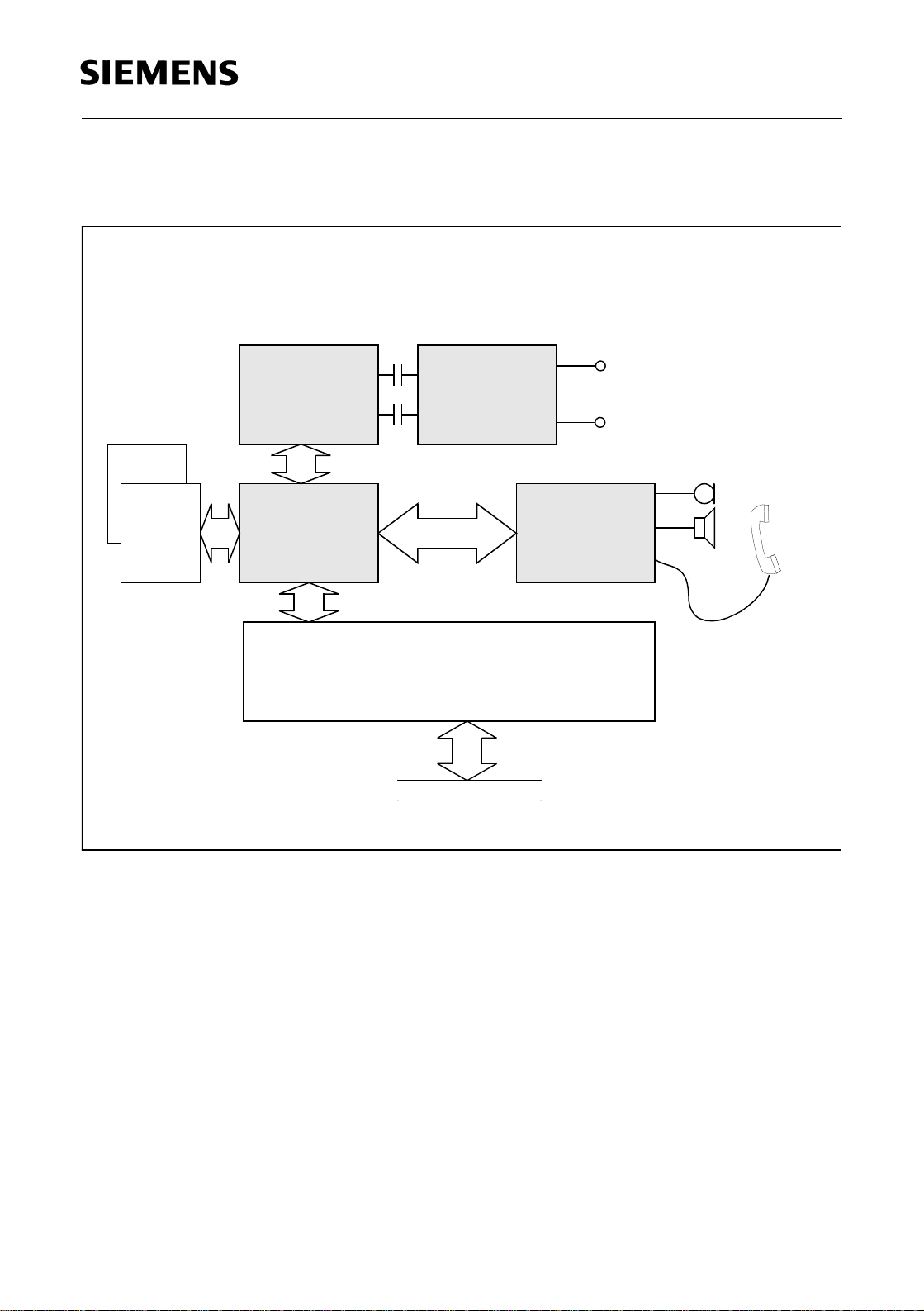
1 Overview
The PSB 4595 and PSB 4596 two-chip solution forms the complete front end of a modem
or fax machine. This Analog Line Interface S olution (AL IS) consists of a DAA, a codec
and a hybrid circuit, and bridges the gap between the phone line and the data pump. The
analog PSB 4595 is manufactured in low-power BiCMOS technology and the digital PSB
4596 in CMOS technology. The ALIS concept is a fully programmable modem front end
which allows a single design for the worldwide market:
• Adaptation to specific countries and applications is achieved by downloading
appropriate coefficient sets.
• Isolation is achieved by a digital capacitor interface, without a transformer; making the
ALIS particularly suitable for designing PCMCIA modems.
• Thanks to an advan ced digital-filter concept in combination with the programmable
electronic DAA, ALIS provides both excellent transmission performance and high
adaptability. This second-generation digital filter concept also allows maximum
autonomy between the various filter b locks. This performance make s ALIS suitable for
V.34+ and V.90 modem applications.
A minimum number of external components is required to complete the functional range
of ALIS. Its internal precision is based on a very accurate band-gap reference. The
frequency behavi or is determined largely by digital filters which exhibit no fluctuations.
As a result of the ADC and DAC concepts, its linearity is limited only by second-order
parasitic effects.
The ALIS chip set can be easily adapted and connecte d to vario us modem data pumps
or to host-based modem solutions. The flexible digital interface of ALIS allows easy
programming via the modem data pump or a controller.
Siemens offers a range of reference and evaluation tools for the ALIS chip set. For
appropriate tools, please contact your nea rest Siemens representative.
Semiconductor Group 7 Data Sheet 06.98
Page 8
Analog Line Interface Solution
ALIS
1.1 Features
• ALIS substitutes data access arrangement (DAA),
codec and hybrid
• Ring detecti on: level, frequency and cadence
• Caller ID: detection, decodi ng and storage
• Programmable to different country requirements
• Programma ble DC characteristics
• ALIS supports V.34+ and V.90
• ALIS complies with ETS 300 001 and FCC
requirements
• Isolation by digital cap acitor interface
• Analog part powered from the tip/ring line by an
integrated voltage regulator
• High performance analog-to-digital and digital-toanalog conversion
• DSP-based solution for adapting the transmission
behavior, especially for
- AC impedance matching
- trans-hybrid balancing
- frequency response
- gain
PSB 4595
PSB 4596
CMOS
P-TSSOP24
P-SSOP28
• Advanced test capabilities:
- digital loops
- analog loops
• High-pass fil te r in rece ive path to suppress line interference (50/60 Hz)
• Isolated control pin s for general purpose use
• Advanced low-po wer 0.8µ m analog B ICMOS technolog y for ALIS analog and 0.8µ m
CMOS technology for ALIS digital
• Two-chip solution: the P-TSSOP24 and P-SSOP28 packages are PCMCIA-compliant
Type Ordering Code Package
PSB 4595 V2.1 P-TSSOP24
PSB 4596 V2.1 P-SSOP28
Semiconductor Group 8 Data Sheet 06.98
Page 9
1.2 Logic Symbol
RESETMCLK
Data
Interface
PSB 4595 / PSB 4596
Analog Line Interface Solution
Isolation
VssVdd
Cap
Interface
µC
Interface
ALIS-D
SO
Caller ID
Interface
Figure 1 Logic Symbol of the ALIS Chipset
ALIS _A
ALIS-A
SO
SI
TIP/RING
Semiconductor Group 9 Data Sheet 06.98
Page 10
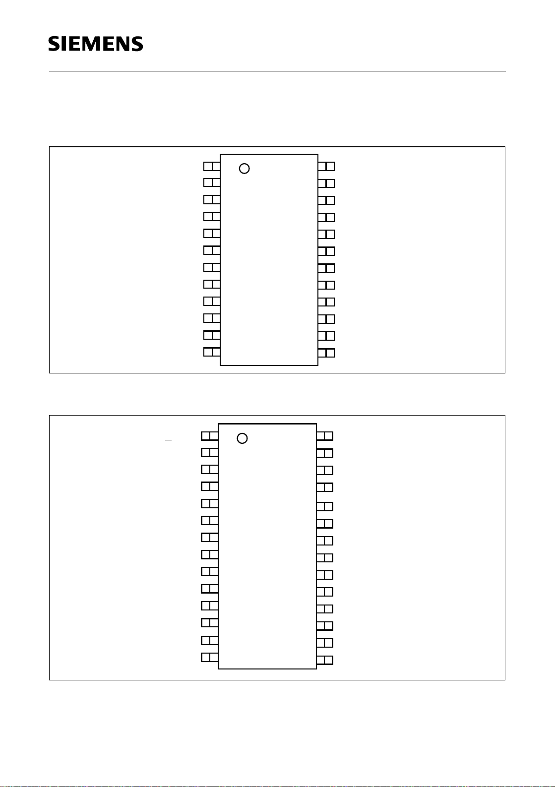
2 Pin Definition and Functions
VDD_SENS
2.1 Pin Configuration
PSB 4595 / PSB 4596
Analog Line Interface Solution
Pin Definition and Functions
CAP1
CAP2
VREF
TIP
TIP_AC
RING
RING_AC
SO_0
SO_1Q
CAP_B22
CAP_B21
CAP_A22
1
2
3
4
5
6
7
8
9
10
11
12
24
23
22
21
20
19
18
17
16
15
14
13
Figure 2 Pin Configuration of ALIS-A (Top View)
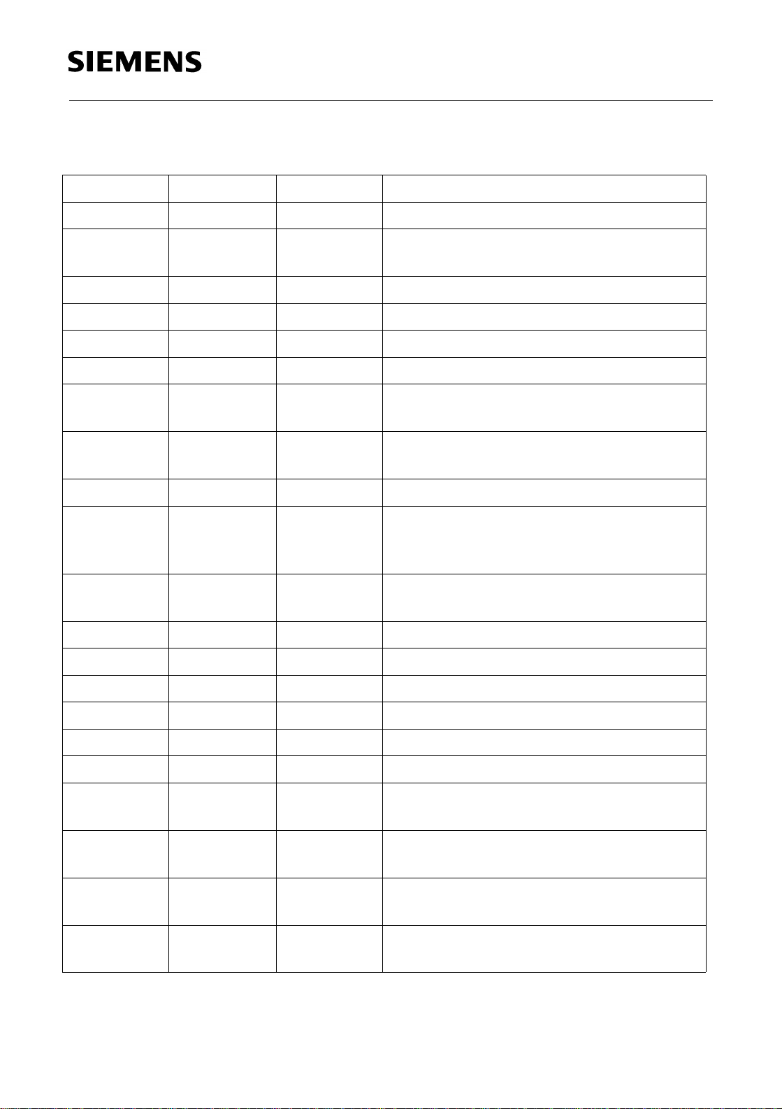
CAP_A12
CAP_B11
1
2
28
27
GNDA
T1G
VDDA
NC
T2G
SI_0
SI_1
TEST
CAP_C21
CAP_C22
CAP_A21
CAP_A11
CAP_C12
CAP_B12
ID_Ain
Afeedback
ID_Bin
Bfeedback
VDD
GND
CS
DCLK
DIN
DOUT
INT
3
4
5
6
7
8
9
10
11
12
13
14
26
25
24
23
22
21
20
19
18
17
16
15
CAP_C11
VDDA
GNDA
RESET
SO
MCLK1
MCLK2
MODE
DAT_CLK
DAT_IN/SEL
DAT_OUT
FSC
Figure 3 Pin Configuration of ALIS-D (Top View)
Semiconductor Group 10 Data Sheet 06.98
Page 11
PSB 4595 / PSB 4596
Analog Line Interface Solution
Pin Definition and Functions
2.2 Pin Definition of ALIS-A PSB 4595
Pin No. Symbol Function Descriptions
22 VDDA Power Programmable supply for the circuitry
24 GNDA Power Analog ground: All signals are referred to
this pin
4 TIP I TIP AC+DC sense input
5 TIP_AC I TIP AC sense input
6 RING I RING AC+DC sense input
7 RING_AC I RING AC sense input
23 T1G O Gate for external transistor T1 (AC/DC
control)
19 T2G O Gate for external transistor T2 (VDDA
control)
21 VDD_SENS I VDDA sense input
3 VREF I/O Reference voltage: Must be connected to
GNDA via an external capacito r of more
than 10 nF (typ. 15 nF)
1 CAP1 I/O Pin for external capacitor of more than 1
µ
F for DC filtering to pin Cap2
2 CAP2 I/O See Cap1
18 SI_0 I Auxiliary input pin 0
17 SI_1 I Auxiliary input pin 1
8 SO_0 O Auxiliary output pin 0
9 SO_1Q O Auxiliary output pin 1
16 TEST I Must be connected permanently to GNDA
13 CAP_A21 I Must be connected via a capacitor of more
than 5pF to CAP_A11.
12 CAP_A22 I Must be connected via a capacitor of more
than 5pF to CAP_A12.
11 CAP_B21 O Must be connected via a capacitor of more
than 5pF to CAP_B11.
10 CAP_B22 O Must be connected via a capacitor of more
than 5pF to CAP_B12.
Semiconductor Group 11 Data Sheet 06.98
Page 12

PSB 4595 / PSB 4596
Analog Line Interface Solution
Pin Definition and Functions
Pin No. Symbol Function Descriptions
15 CAP_C21 I Must be connected via a capacitor of more
than 5pF to CAP_C11.
14 CAP_C22 I Must be connected via a capacitor of more
than 5pF to CAP_C12.
Table 1: ALIS-A Pin Definition
Semiconductor Group 12 Data Sheet 06.98
Page 13

PSB 4595 / PSB 4596
Analog Line Interface Solution
Pin Definition and Functions
2.3 Pin Definition of ALIS-D PSB 4596
Pin No. Symbol Function Description
8 VDD Power +5 Volt supply for the digital circuitry
9 GND Power Ground digital: All sig nals are referred to
this pin
25 VDDA Power +5 Volt supply for the analog circuitry
24 GNDA Powe r Ground analog: All analog signals are
referred to this pin
21 MCLK1 I Master clock1: One pin of a crystal or
ceramic resonator is connected. This pin
can also be driven from an external
clocking source of 16.384 MHz,
synchronous to FSC (MCLK=FSC*2048)
20 MCLK2 O Master clock2: The other pin of a crystal or
ceramic resonator is connected. When
MCLK1 is driven by an external clock, this
pin should be left open
23 RESET I Reset input: Forces the device to default
mode (low active)
15 FSC BI As input: Frame synchronisation clock,
8kHz, identifies the beginning of the
frame. FSC must be synchronous to
MCLK (MCLK=FSC*2048)
As Output: Indicates the beginning of a
new frame
17 DAT_IN /
SEL
16 DAT_OUT O Data interface: Transmit data to the DSP.
I Data interface: Receive data from the
DSP. The data is received in 16-bit bursts
every 125 ms.
Interface selection pin in MUX mode.
The data is transmitted in 16-bit bursts
every 125 ms
18 DAT_CLK I Data clock 128 to 1024 kHz: Determines
the rate at which data is shifted into or out
of the data interface
10 CS I µ-controller interface: Chip select enable
to read or write data. Active low
Semiconductor Group 13 Data Sheet 06.98
Page 14
Analog Line Interface Solution
Pin No. Symbol Function Description
PSB 4595 / PSB 4596
Pin Definition and Functions
11 DCLK I
12 DIN I
13 DOUT TRI
14 INT O
19 MODE I Interface mode pin (parallel or MUX
4 ID_Ain I Input for caller ID comparator (connection
6 ID_Bin I
5 A feedback O Feedback for caller ID comparator
7 B feedback O Feedback for caller ID comparator
28 CAP_A11 O Must be connected via a capacitor of more
1 CAP_A12 O Must be connected via a capacitor of more
µ
-controller interface: Clock. Maximum
clock rate 1024 kHz
µ
-controller interface: Input data
µ
-controller interface: DOUT is high ’Z’ if
no data is transmitted
µ
-controller interface: Interrupt output pin
mode)
to TIP)
Input for caller ID comparator (connection
to RING)
than 5pF to CAP_A21.
than 5pF to CAP_A22.
2 CAP_B11 I Must be connected via a capacitor of more
than 5pF to CAP_B21.
3 CAP_B12 I
26 CAP_C11 O Must be connected via a capacitor of more
27 CAP_C12 O Must be connected via a capacitor of more
22 SO O Auxiliary output pin
Table 2: ALIS-D Pin Definition
Must be connected via a capacitor of more
than 5pF to CAP_B22.
than 5pF to CAP_C21.
than 5pF to CAP_C22.
Semiconductor Group 14 Data Sheet 06.98
Page 15
PSB 4595 / PSB 4596
Analog Line Interface Solution
System Integration
3 System Integration
ALIS can be used in different modem applicati ons to connect the data pump to the TIP /
RING wire.
3.1 ALIS with DSP-based Modem
For a modem data pump, the ALIS pro vides the front-end to the tip/ring.
Data Pump
V.34
V.90
ALIS-D
SI
PSB 4596
ALIS-A
Tip/Ring
PSB 4595
Note: SI: Serial Interface
Figure 4 DSP-based Modem Application
Isolation is provided by a capacitor inte rface, without transformer. This allows ver y flat
frequency response over the entire voice band, even at low frequencies.
In V.90 Modem applications, the 50/60 Hz hig h-pass filter can be turned off.
Semiconductor Group 15 Data Sheet 06.98
Page 16
PSB 4595 / PSB 4596
Analog Line Interface Solution
System Integration
3.2 ALIS with Software Modem
ALIS also supports software modems wh ere V.34 runs on the host computer (e.g. in
combination with a USB controller).
ALIS-D
PSB 4596
SI
Microcontroller with USB or PCI Interface
USB or PCI
Figure 5 Software Modem Application
ALIS-A
Tip/Ring
PSB 4595
Semiconductor Group 16 Data Sheet 06.98
Page 17
PSB 4595 / PSB 4596
Analog Line Interface Solution
System Integration
3.3 Hybrid Modem (ISDN plus Analog)
In combination with the SIEMENS ISDN chip set, ALIS supports hybrid modems, ,
allowing connection to either the TIP/RING line or to an S or U-interface for ISDN
applications.
ALIS-A
Tip/Ring
PSB 4595
ISAC-S TE
S-Interface *IOM-2 Interface
PSB 2186 *
Flash
SRAM
ALIS-D
PSB 4596
SI
ISAR34
PSB 7115
Microcontroller with USB or V.24 In te rface
USB or V.24
Figure 6 Hybrid Modem Application, with S-interface: ISAR34 Enhanced Data Access Controller (PSB 7115) and ISDN Access Co ntroller for S-Bus ISAC-S TE (PSB
2186)
* Figure 4 shows a hybrid modem with the ISDN S-interface. To meet the ISDN Uinterface, the ISAC-S TE PSB 2186 is repla ced by the IEC-Q TE PSB 21911.
Semiconductor Group 17 Data Sheet 06.98
Page 18
3.4 Modem with Speakerphone
PSB 4595 / PSB 4596
Analog Line Interface Solution
System Integration
Flash
SRAM
ALIS-D
PSB 4596
SI
ISAR34
IOM-2 Interface
PSB 7115
ALIS-A
TIP/RING
PSB 4595
ARCOFI-SP
PSB 2163
Microcontroller with USB or V.24 Interface
USB or V.24
Figure 7 Application wi th Speakerphone: ARCOFI-SP Audio Ringing Codec (PSB
2160, PSB 2163, PSB 2165, PSB 2168) and ISAR34 Enhanced Data Access Controller (PSB 7115)
Semiconductor Group 18 Data Sheet 06.98
Page 19
PSB 4595 / PSB 4596
Analog Line Interface Solution
System Integration
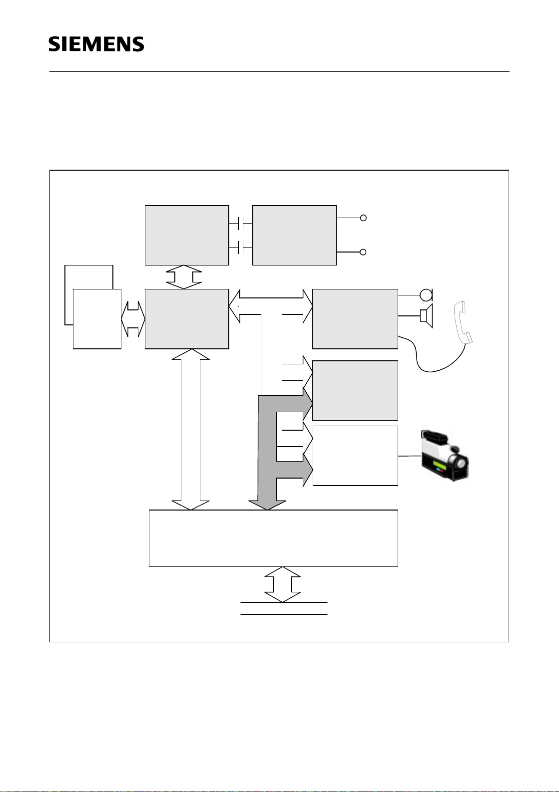
3.5 Analog Videophone
The diagram below shows a system solution for an analog videophone application using
a SIEMENS chip set.
Flash
SRAM
ALIS-D
PSB 4596
SI
ISAR34
PSB 7115
ALIS-A
PSB 4595
IOM-2 Interface
Tip/Ring
ARCOFI-SP
PSB 2163
JADE AN
PSB 7230
VIDEO
CODEC
Microcontroller with USB or V.24 Interface
USB or V.24
Figure 8 ARCOFI-(SP) Audio Ringing Codec (PSB 2160, PSB 2163, PSB 2165, PSB
2168) ; ISAR34 Enhanced Data Access Controller (PSB 7115); JADE Joint Audio
Decoder Encoder (PSB 7230, PS B 723 8)
Semiconductor Group 19 Data Sheet 06.98
Page 20
PSB 4595 / PSB 4596
Analog Line Interface Solution
ALIS Implementation
4 ALIS Implementation
The ALIS chip set repla ces all the major parts of a conventional front end for mod em
solutions. The circuit consists of two major parts, a DSP-based codec and an electronic
DAA. Advanced features such as ring detection, pulse dialing and caller ID are
integrated on-chip. Additional operating modes such as sleep mode or ringing mode are
implemented to minimize power consumption .
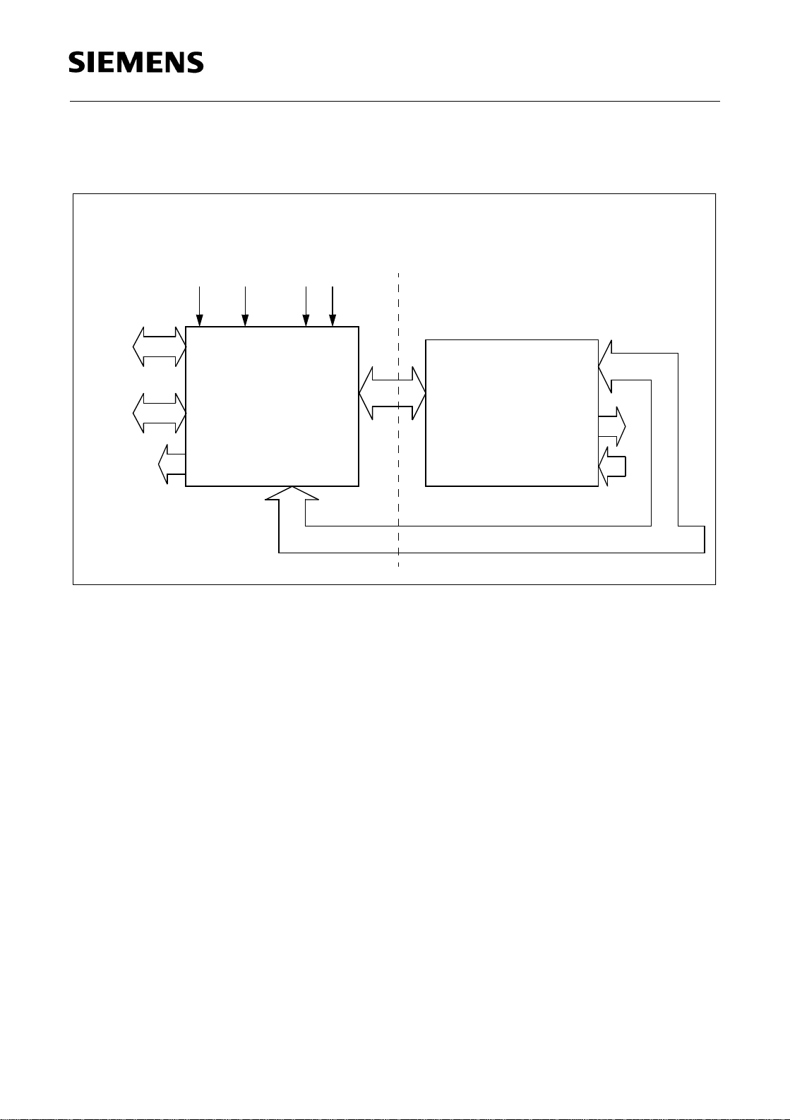
4.1 ALIS Block Diagram
The tip/ring telephone line interface is connected mainly with the ALIS-A. It is also
connected with the ALIS-D for Caller ID functions..
Control Data
Control Interfac e
DSP
Data Interface
Transmit/Receive Data
HWFilter
Caller ID
Isolation
Cap. Int erface
A/D
D/A
I/O
Vdd
Control
Hybrid
and
Filters
ALIS-AALIS-D
Control
TIP/RING
Figure 9 ALIS Block Diagram
The analog front end (ALIS-A) is connected t o the line via TIP/RING. The programmable
supply voltage for AL IS-A is generate d from the line by the Vdd control. Two/four wire
conversion is implemente d in the hybrid circuit. Ana log anti-aliasing pre -filters (PREFI)
and smoothing post-filters (POFI) are included for signal conditioning. High-performance
over-sampling analog-to-digital converters (ADCs) and digital-to-analog converters
(DACs) assure the required conversion accuracy. The ADCs and DACs are connected
to the digital signal processor (DSP) on the digital part (ALIS-D) via a dedicated capacitor
interface which also provides the requi red isolation to the line . Special hardwa re filters
perform filtering functions such as interpolation and decimation. The DSP handles all the
necessary algorithms. These include bandpass filtering, sample rate conversion, ringing
detection, and caller ID decoding. All programmable filters and functions are also
controlled and processed by the DSP. The control interface allows external control of the
ALIS features and provide s transp arent access to ALIS commands an d signaling pin s.
Thus pre-calculated sets of coefficients can be downlo aded from the system to the o n-
Semiconductor Group 20 Data Sheet 06.98
Page 21
PSB 4595 / PSB 4596
Analog Line Interface Solution
ALIS Implementation
chip coefficient RAM (CRAM) in order to progr am the fil ters. Transmit an d receive data
is transferred to and from the data pump via the data interfa ce .
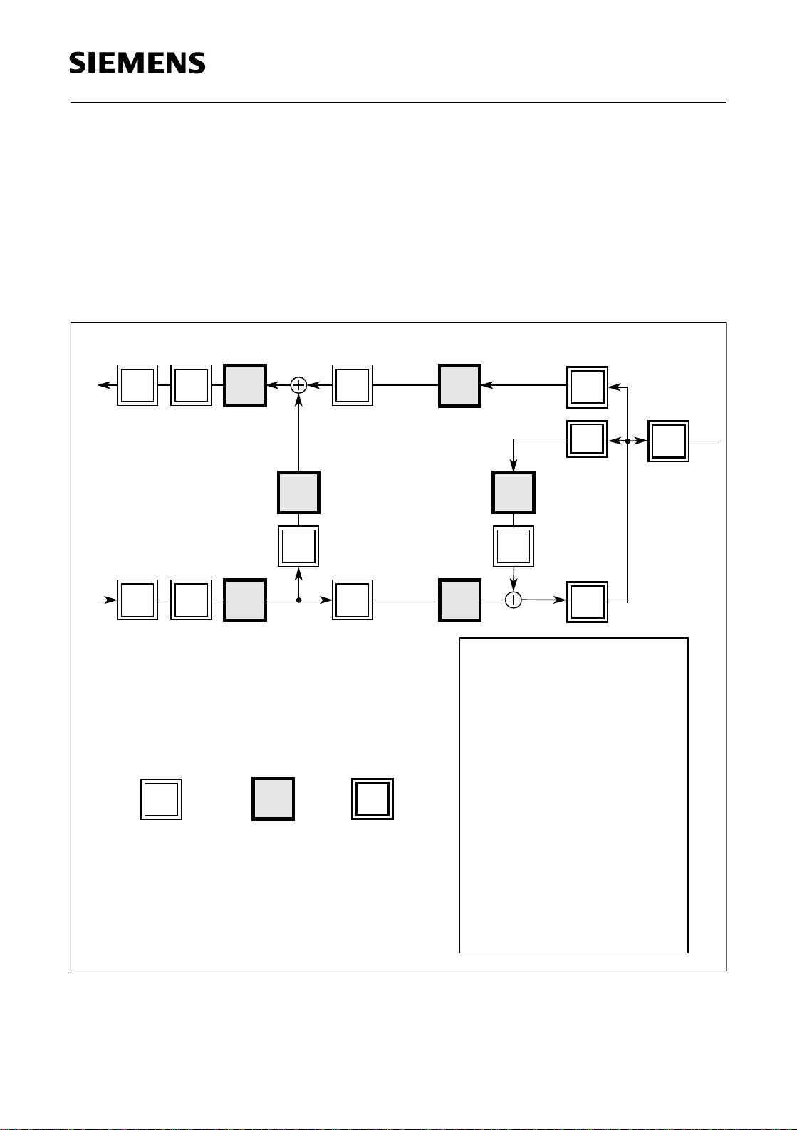
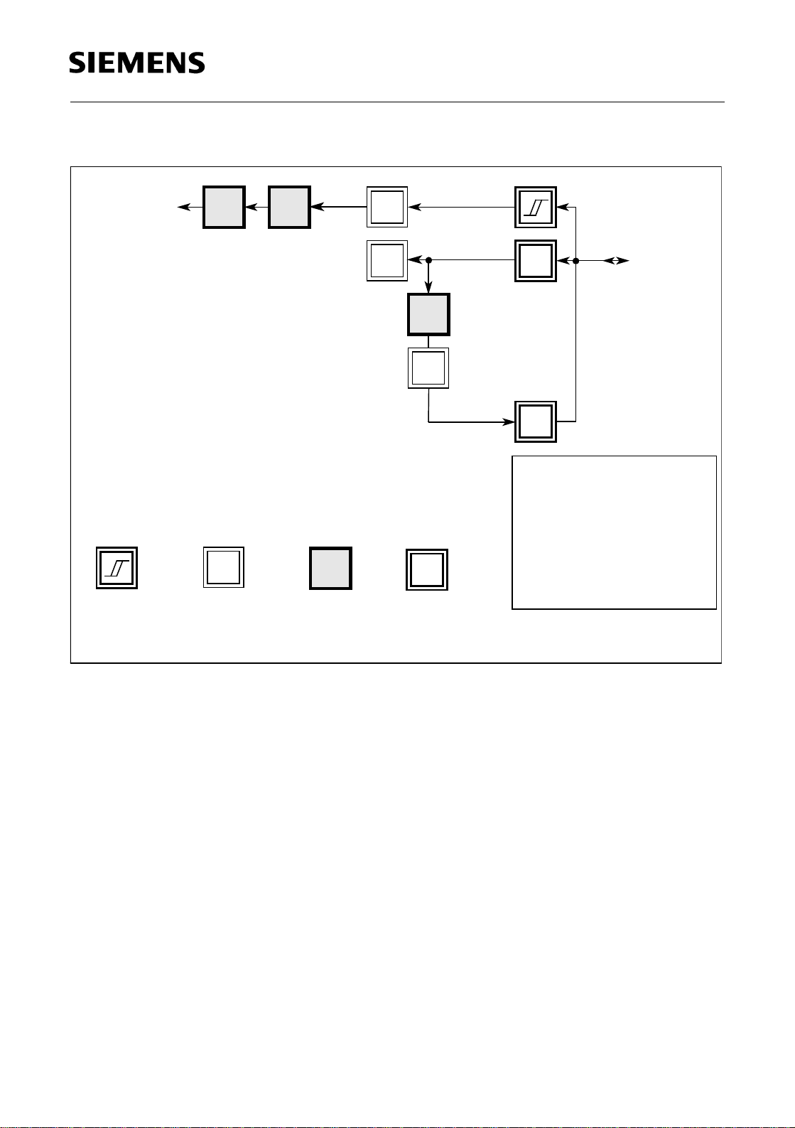
4.2 ALIS AC Signal Flow Graph
ALIS architecture is based on digital filters. The data path through these filters is shown
in the next few diagrams. The filter concept also allows maximum autonomy between the
different filter blocks. Each filter block has a one -to-one corresp onden ce with a specific
network element. Marked filters (gre y) can be programmed by the user.
digital out
FRRAR1
digital in
user-programmable block
Definition:
Transmit:Digital-to-Analog
Receive :Analog-to-Digital
RFIX1
XFIX1FRXAX1
fixed filter block
THFIX
TH
AR2
AX2
fixed functional block
RFIX2
XFIX2
Legend:
DAA
AR1
FRR
RFIX1
AR2
RFIX2
ADC
THFIX
TH
IMFIX
IM
AX1
FRX
XFIX1
AX2
XFIX2
DAC
ADC
ADC
IMFIX
IM
DAC
Data Access Arrangement, Fix ed Part
Amplification Receive Filter 1
Equalizatio n Rec e iv e
Receive Filter Fixed Part 1
Amplification Receive Filter 2
Receive Filter Fixed Part 2
Analog-to-Digital Converter
Transhybrid Filter Fix ed Part
Transhybrid Filter
Impedance Filter Fixed Part
Impedance Filter
Amplification Transmit Filter 1
Equalization Trans m it
Transmit Filter Fixed Part 1
Amplification Transmit Filter 2
Transmit Filter Fixed Part 2
Digital-to-Analog Converter
DAA
Tip/
Ring
Figure 10 AC Signal Flow Graph
Semiconductor Group 21 Data Sheet 06.98
Page 22

PSB 4595 / PSB 4596
Analog Line Interface Solution
ALIS Implementation
4.2.1 Receive Path
After passing the DAA and a simple anti-aliasing pre-filter with an analog gain stage, the
voice signal is converted to a 1-bit digital data strea m in the sigma-delta converte r. The
first down-sampling steps are performed in fast digital hardware filters. Subsequent
processing is implemented in the digital structure which allows easy and flexible
programming of parameters. Finally, the fully processed signal is transferred to the data
interface.
Subsequent processing is done by microcode in the digital filter structure to allow
adaptability. Gain adjustment is pro vided in two stages, AR1 and AR2. The total gain
adjustment is programmable in two ranges: from 14 to 24 dB, in steps of 0.5 dB; and from
-3 to 14 dB, with steps between 0.02 and 0.05 dB.
Located inbetween is a decimation stage to reduce the sampling rate to the 8 kHz PCM
rate, and a low-pass filter to band-limit the signal in accord ance with ITU-T G.714 and
ETSI (NET33) recommendations (in RFIX1); also an equalization stage (in FRR).
Finally, the signal is passed out to the Serial Data Interface (SDI).
ALIS meets or exceeds all ITU and ETSI (NET33) recommendations on attenuation
distortion and group delay.
4.2.2 Transmit Path
The digital input signal is received via the data interface. Low-pass filtering, gain
correction and frequency-response correction are implemented in the digital filter
structure. The up-sampling in terpolation is then performed by fast hard ware structures
to reduce the DSP load. The up- sampled 1-bit data stream is converted to an analo g
equivalent which is smoothed by a post-filter (POFI) and conv erted to a 2-wire signal in
the DAA.
There are also two independent tone generators which can insert tones into the Transmit
path. They have adjustable frequencies, default 2 kHz, and a programmable bandpassfilter to adapt the output for DTMF. When either tone generator is on, the data signal
transmission is suppressed.
4.2.3 Loops
ALIS implementation inclu des two loops. One is used to generate the AC-terminatio n
impedance (IM) and the other is used to perform proper hybrid balancing (TH). A simple
additional path IM (from the receive to the transmit path) supports the impedancematching function.
4.2.4 Test Features
Several analog and digital test loops are implemented in ALIS. The receive and transmit
paths may be short-circuited at two different points for test purposes.
Semiconductor Group 22 Data Sheet 06.98
Page 23
Analog Line Interface Solution
4.3 ALIS Ring and Caller ID Signal Flow Graph
PSB 4595 / PSB 4596
ALIS Implementation
CID out
comparator for CID
CIDL
user-programmabl e block
CIDH
fixed filter block
CIDBP
RLM
RIM
FIX
RIM
fixed functional block
Tip/Ring
ADC
DAC
Legend:
Caller ID Lowpass
CIDL
Caller ID Hilbert Transformer
CIDH
Caller ID Bandpass
CIDBP
RLM
Ring Level Metering
Analog-to-Digital Converter
ADC
Ringer Impedace Filter Fixed Part
RIMFIX
Ringer Impedace Filter
RIM
DAC
Digital-to-Analog Converter
Figure 11 Ring Signal Flow Graph
These data paths operate only when the A LIS is in Ringi ng state.
4.3.1 Caller ID (CID) Path
The Caller ID receiver meets Bellcore specifications TR-NWT-000030 and
SR-TSV-002476 for Caller ID. In this service, the calling party’s information (Calling Line
Identification Presenta tion (CLIP)) is transmitted in the silent interva l between the first
and second ring. ALIS receives and stores up to 4096 bits of the 1200 baud FSK
(Frequency Shift Keying) signal. The decodi ng scheme meets the Bell 202 and ITU-T
V.23 specifications.
The FSK signal which contains the caller information is converted to a 1-bit data stream
by a comparator in order to minimize power consumption. Down-sampling steps are
performed in fast digital hardware filters. To decode the caller ID, bandpass filtering,
Hilbert transformation and other functions are implemented. The output CID-out is
sampled at 1200 baud, an d stored in the CID-RAM.
Semiconductor Group 23 Data Sheet 06.98
Page 24

PSB 4595 / PSB 4596
Analog Line Interface Solution
ALIS Implementation
4.3.2 Ring-Level Metering (RLM) Path
The analog signal is converted to a 1-bit data stream in the ADC. After decimation in
hardware filters, the remaining processing is done in the digital filter structure (in RLM):
bandpass filtering to select the ringing frequency, and integration to determine if the
amount of energy in-band has exceeded the threshold for a valid ring signal. The
bandpass parameters and threshold are programmable.
Ringing is detected in this path. Th e digital input is bandpass filtered, integrated and
compared to a threshold to determine if a ringing signal has occurred. The threshold and
bandpass filters are programmab le. The result of this operation can be monito red by
reading the RMR bit (see “CR1 Configuration Register 1 (Diali ng)” on page 40).
4.3.3 Loops
A loop is available to generate the Ring-termination impedance (RIM).
4.3.3.1 Test Features
There are three loopbacks on ALIS-D to test interfaces:
- Host interface: loopback from the PCM in te rface (just inside ALIS-D)
- Caller ID interface: loopback from Caller ID input to capacitor interface
- Capacitor interface: loopb ack throug h different parts of the capacitor interface
There are two loopbacks on ALIS-A:
- Tip/ring interface: loopback from the tip/ring, before the ADC
- Codec: loopback from the tip/ring, after the codec
Semiconductor Group 24 Data Sheet 06.98
Page 25
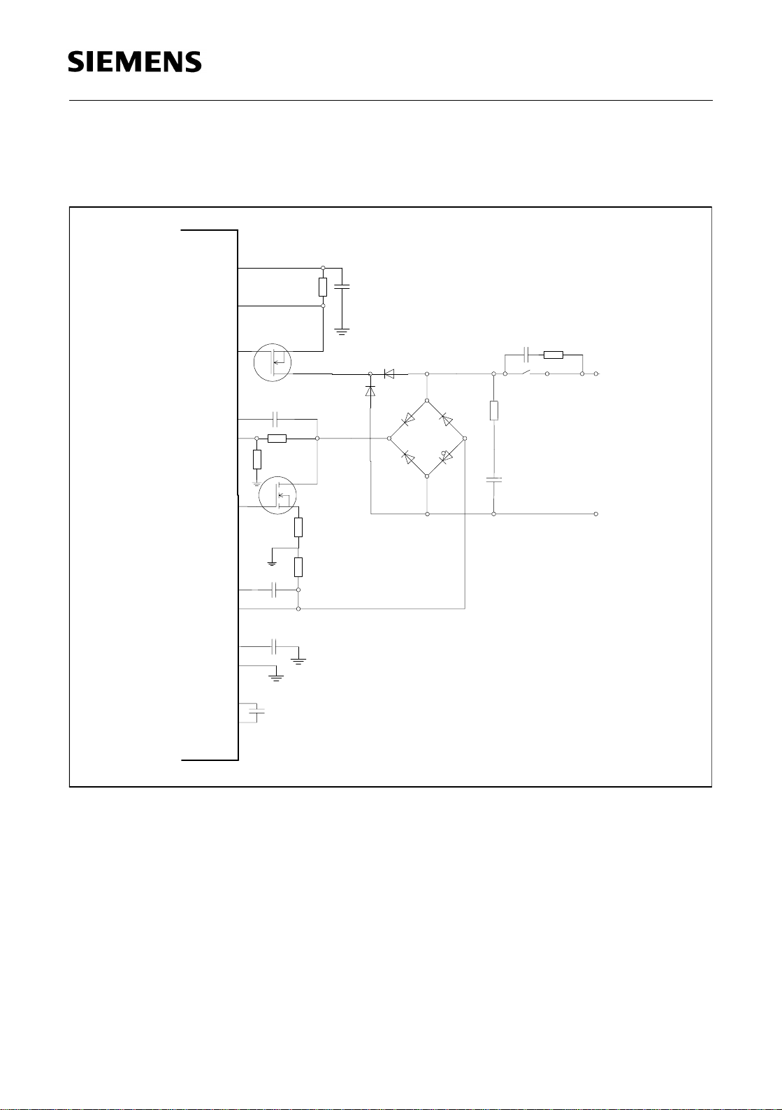
5 Configuration Overview
5.1 Connection to the Telephone Line
VDDA
SENS
VDD
T2
T2G
-
AC
TIP
TIP
PSB 4595 / PSB 4596
Analog Line Interface Solution
Configuration Overview
TIP
T1
T1G
RING-AC
RING
VREF
GNDA
CAP1
CAP2
RING
Figure 12 Connection of ALIS-A to the Telephone Line
As shown in the figure, ALIS-A requires a minimum of components to complete the DAA:
- Protection circuit: not shown.
- Bridge: using Schottky diodes will improve the performance at low feedin g condition s.
Recommended: Dual Schottky diode SIE M ENS BAT 240A.
- Resistors for current sensing.
- Capacitors for AC coupling and VDD buffering.
Semiconductor Group 25 Data Sheet 06.98
Page 26

PSB 4595 / PSB 4596
Analog Line Interface Solution
Configuration Overview
- Two transistors (T1, T2) to handle the line current. T2 must be of depletion type, in order
to deal with start-up. Recommen ded tran sistors: T1: SIE MENS BS P 88; T2: SIEMENS
BSP 129.
- Components for EMC protection: no t shown, as they depend on the board layout.
ALIS-D can optionally be connected to the tip/ring to provide Caller ID functions. The CID
circuit requires two capacitors and four resistors.
5.2 Host Interface
The host interface consists of a serial µ-controller interface and a 16-bit linear data
interface. They are used to connect ALIS either to a
The two serial interfaces can be accessed on two separate serial ports or in timemultiplex (MUX) mode on a single serial port.
5.2.1 The µ-Controller Interface
µ
-
controller and or to a data pump.
The ALIS internal con figuration registers, the auxiliary po rts, and the Coefficient RAM
(CRAM) are programmable via the serial µ-controller interface. This interface consists of
four pins:
CS: Chip select, to enable inte rface (active low)
DCLK: Clock, 1 kHz to 1024 kHz
DIN: Data input
DOUT: Data output
CS is used to start serial access to the ALIS registers and the Coefficient RAM. Following
a CS falling edge, the first eight bits received at DIN specify the command. Subsequent
data bytes (the number depends on the command) are stored in the selected
configuration registers or th e selected part of the CRAM.
Serial interface specification: 8 bit, no parity, no start/stop bit. Every command must
begin with a CS falling edge.
Semiconductor Group 26 Data Sheet 06.98
Page 27
CS
DCLK
PSB 4595 / PSB 4596
Analog Line Interface Solution
Configuration Overview
DIN
36547 210 36547 210
36547 210
Control Data Byte 1 Data Byte 2
High ’Z’
DOUT
Figure 13 Example of a Write Access, two Data Bytes transferred
If the first eight bits received via DIN specify a read command, ALIS will start to respond
via DOUT with its specific identification byte. The number of specified d ata bytes within
the command (contents of configuration registers or contents of the CRAM) will follow on
DOUT.
CS
DCLK
DIN
36547 210
Control
High ’Z’
DOUT
36547 210
36547 210
Identification Data Byte 1
Figure 14 Example of a Read Access, one Data Byte transferred via DOUT
Semiconductor Group 27 Data Sheet 06.98
Page 28
PSB 4595 / PSB 4596
Analog Line Interface Solution
Configuration Overview
The data transfer is synchronized by DCLK. DIN is latched at the falling edge of DCLK,
while DOUT changes with the rising edge of DCLK. During the execution of a command
which is followed by output data (read command), the device will not accept any new
command via DIN. The data transfer sequence can be interrupted by setting CS to ’1’.
To reduce the number of connections to the µ-processor, DIN and DOUT may be
strapped together to form a bi-directiona l data pin.
5.2.2 The Data Interface
A serial data inte rface is used for tran sferring voice data. The inte rface consists of five
pins:
DAT_CLK: Clock, 128 kHz to 1024 kHz
FSC: Frame synchronization clock, 8 kHz
DAT_IN: Transmit data input
DAT_OUT: Receive data output
The Frame Sync (FSC) pulse identifies the beginning of a receive and a transmit frame.
DAT_CLK synchronizes the data transfer on DAT_IN and DAT_OUT. The data bytes are
first serialized to 16-bit width and MSB. The rising edge indicates the start of the bit, while
the falling edge is used to latch the conten ts of the received data.
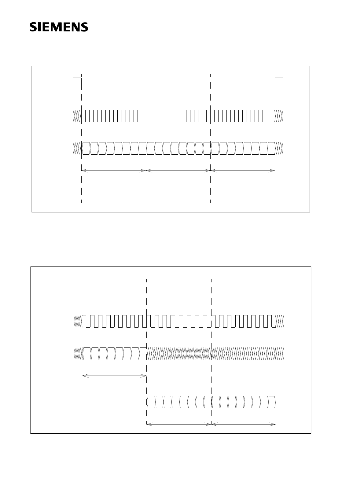
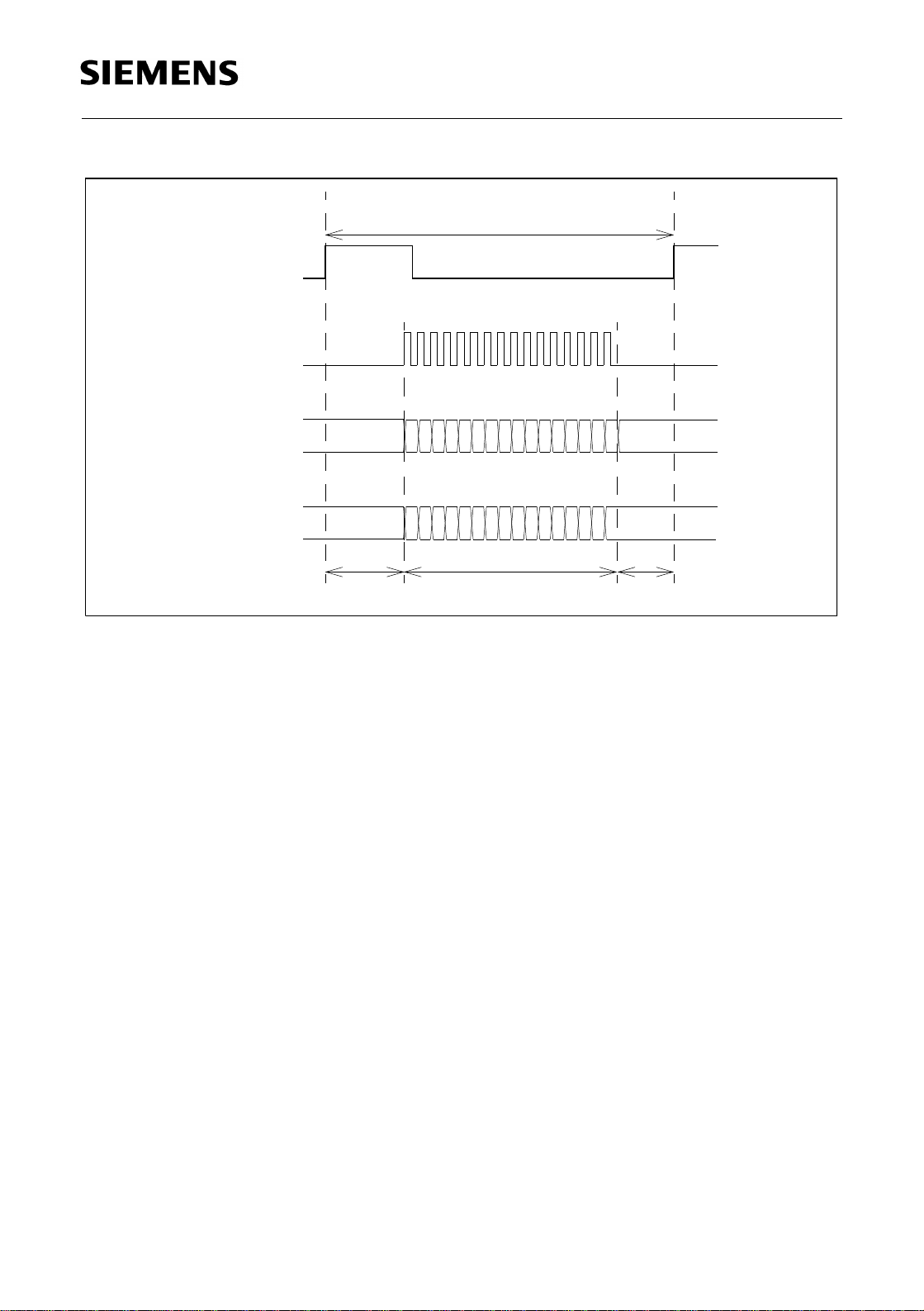
125 µS
FSC
DAT_CLK
DAT_IN
DAT_OUT
0
0
1114 13 1215 10 9 8 36547 210
1114 13 1215 10 9 8 36547 210
16 Bit Voicedata MSB first
12
12
Figure 15 Example of a Clock Rate of 128 kb/s
Semiconductor Group 28 Data Sheet 06.98
Page 29
FSC
DAT_CLK
PSB 4595 / PSB 4596
Analog Line Interface Solution
Configuration Overview
125 µS
DAT_IN
DAT_OUT
1114131215 10 9 8 36547 210
1114131215 10 9 8 36547210
Voice
t
tStoptStart
Figure 16 Example of a Clock Rate higher than 128 kb/s
The data package must stay within the frame, t
> 0 and t
Start
Stop
> 0.
The FSC signal can be generated externally by the ho st or by ALIS.
Semiconductor Group 29 Data Sheet 06.98
Page 30
PSB 4595 / PSB 4596
Analog Line Interface Solution
Configuration Overview
5.2.3 Interface Modes
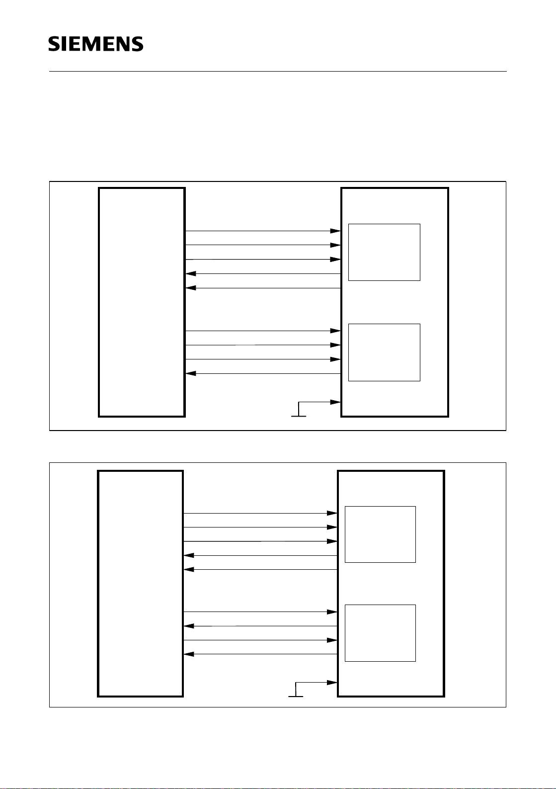
5.2.3.1 Demux Mode
Connection of the MODE pin to GND allows the µC and the data interface to be
accessed via two serial ports.
DSP
(Data Pump)
DCLK
CS
DIN
DOUT
INT
DAT_CLK
FSC
DAT_IN
DAT_OUT
MODE
Figure 17 Host Interface in Demux Mode, FSC as Input
DSP
(Data Pump)
DCLK
CS
DIN
DOUT
INT
µC Interface
ALIS-D
µC Interface
Data
Interface
ALIS-D
DAT_CLK
FSC
DAT_IN
DAT_OUT
Data
Interface
MODE
Figure 18 Host Interface in Demux Mode, FSC as Output
Semiconductor Group 30 Data Sheet 06.98
Page 31

PSB 4595 / PSB 4596
Analog Line Interface Solution
Configuration Overview
5.2.3.2 Multiplex Mode
Connection of the MODE pin to VDD allows the two interfaces to be time-multiplexed on
a single port. The interfaces are selected by the DAT_IN/SEL pin.
DSP
(Data Pump)
DCLK / DAT_CLK
CS / FSC
DIN / DAT_IN
DOUT / DAT_OUT
INT
DAT_IN / SEL
VDD
Figure 19 Host Interface in MUX Mode, FSC as Input
DAT_IN / SEL = 0 DAT_IN / SEL = 1
ALIS-D
µC Interface
Data
Interface
MODE
PIN No Function PIN No Function
11 DCLK 11 DAT_CLK
10 CS 10 FSC
12 DIN 12 DAT_IN
13 DOUT 13 DAT_OUT
Table 3: Pin Definition in MUX mode, FSC as Input
Semiconductor Group 31 Data Sheet 06.98
Page 32

PSB 4595 / PSB 4596
Analog Line Interface Solution
Configuration Overview
DSP
(Data Pump)
DCLK / DAT_CLK
CS
DIN / DAT_IN
DOUT / DAT_OUT
INT
FSC
DAT_IN / SEL
VDD
Figure 20 Host Interface in MUX mode, FSC as Output
DAT_IN / SEL = 0 DAT_IN / SEL = 1
ALIS-D
µC Interface
Data
Interface
MODE
PIN No Function PIN No Function
11 DCLK 11 DAT_CLK
10 CS 10 VDD / GND
12 DIN 12 DAT_IN
13 DOUT 13 DAT_OUT
15 FSC (output) 15 FSC (output)
1) must be connected to a fixed potential
Table 4:
Pin Definition in MUX Mode, FSC as Output
1)
Semiconductor Group 32 Data Sheet 06.98
Page 33

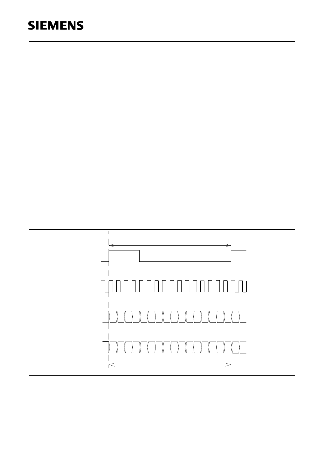
MUX-Mode, FSC extern
FSC
DCLK = DCLK/DAT_CLK
CS = CS/FSC
DIN= DIN/DAT_IN
DOUT= DOUT/DAT_OUT
PSB 4595 / PSB 4596
Analog Line Interface Solution
Configuration Overview
C o n tr o l D a ta
Clock in Clock in
Clock out Clock out
DAT_IN = SEL
MUX-Mode, FSC intern
FSC
DCLK = DCLK/DAT_CLK
CS = CS
DIN= DIN/DAT_IN
DOUT= DO UT/DAT_O UT
DAT_IN = SEL
UC M ODE
rising edge cs w ith sel=1 is fsc start
C o n tr o l D a ta
Clock inClock in Clock in
Clock out Clock ou t
Clock out Clock ou t
PCM MODE
125 us FR AM E
Clock in
PCM MODE
125 us FR AM E
Figure 21 Protocol for Transmission of µC- and PCM Data in MUX Mode
5.3 Clocking
ALIS operates with a typical master clock frequency of 16.384 MHz. This clock can eit her
be supplied from an external source or generated with a crystal by AL IS-D.
It is essential that the ratio of the master clock frequency to the FSC frequency is exactly
2048. This is of course guaranteed if the FSC signal is generated internally.
5.3.1 External clock
When providing the master clock externally, an external clock signal must be connected
to pin MCLK1. The MCLK2 pin must remain unconnected and the CL K_EXT bit in CR0
must be programmed to a logic ’1’. (see the section “CR0 Configuration Register 0
(Filters)” on page 39).
Semiconductor Group 33 Data Sheet 06.98
Page 34

PSB 4595 / PSB 4596
Analog Line Interface Solution
Configuration Overview
5.3.2 Crystal clock
Because ALIS i ncludes an on-chip oscillator cir cuit, an external crystal may be used.
This crystal is connected across the MCLK1 and MCLK2 pins with two capacito rs (see
Figure 22 ”External Crystal Connections” ) . The CLK_EXT bit in CR0 must be
programmed to a logic '0' (= default value after reset). The capacitor valu es depend on
the crystal type a nd are sp ecified by the crystal manu factu rer. A mi cropr ocessor-grade
crystal with a parallel-resonant fu ndamental frequen cy is recommended.
To ensure that the ratio between the master clock and the FSC signal is correct, A LIS
can be programmed to internal FSC generation (set Fsc_en bit in CR4 to a logic '1'). See
Figure 18 “Host Interface in Demux Mode, FSC as Output” on page 30 and Fi gure 20
“Host Interface in MUX mode, FSC as Output” on page 32.
XTAL 16.384 MHz
C
xtl
MCLK1
ALIS-D
Figure 22 External Crystal Connections
C
MCLK2
xtl
Semiconductor Group 34 Data Sheet 06.98
Page 35

PSB 4595 / PSB 4596
CAP_A21
CAP_A22
CAP_B21
CAP_B22
CAP_C21
CAP_C22
Analog Line Interface Solution
Configuration Overview
5.4 Capacitor Interface
A capacitor interface is used to decouple ALIS-A from ALIS-D. It is a bi-directional serial
interface and is used for exchangin g control and data infor mation between A LIS-A and
ALIS-D. The transmission format is digital to avoid distortion and for performance
reasons. For the size and tolerance of the capacitors, see the section “ALIS Cap
Interface” on page 86.
CAP_A11
CAP_A12
CAP_B11
CAP_B12
CAP_C11
CAP_C12
ALIS-D
CAP_A1
CAP_A2
CAP_B1
CAP_B2
CAP_C1
CAP_C2
ALIS-A
Figure 23 Connection of Capacitor Interface between ALIS-A and ALIS-D
Semiconductor Group 35 Data Sheet 06.98
Page 36

PSB 4595 / PSB 4596
Analog Line Interface Solution
Configuration Overview
5.5 Caller ID Interface
To receive the caller ID, ALIS-D must be connected to the line via an RC network. See
the section “ALIS Caller ID Interface” on page 86" .
Afeedback
ID_Ain
ID_Bin
Bfeedback
Rfb1
Rin1
Rin2
Rfb2
Cin1
Cin2
ALIS-D
Figure 24 Caller ID Interface Connection of ALIS-D to Tip/Ring
TIP
RING
Semiconductor Group 36 Data Sheet 06.98
Page 37

PSB 4595 / PSB 4596
Analog Line Interface Solution
Programming ALIS
6 Programming ALIS
Appropriate commands via the serial µ-controller interface enable very flexible
programming and verificatio n of ALIS.
Four different commands are used to a ccess the various control registers and RA Ms:
SOP (see page 38), XO P (see page 44), COP (see page 50) and CAO (see page 51) .
The first byte received via DIN selects the command type. Each command can be used
as a write or read command. Th anks to the extended ALIS control facil ities, the SOP,
XOP and COP commands contain add itional in formation fo r progr amming (writing ) an d
verifying (reading) the ALIS status (e.g . number of subsequent bytes, software reset,
operating mode).
Up to 8 bytes of data can b e read o r written wi th an S OP , XO P or COP co mmand. Th e
CAO command allows all 512 bytes of the caller ID RAM to be read or written. Any read
command causes ALIS to respond with its specific identification byte before sending the
requested information.
6.1 Types of Commands and Data Bytes
The ALIS commands are se lected by bit 3, 4 and 6 of the command byte as sh own
below.
SOP command
Bit76543210
PU 1 PU 0 RW 1 0 LSEL2 LSEL1 LSEL0
XOP command
Bit76543210
RST 0 RW 1 1 LSEL2 LSEL1 LSEL0
COP command
Bit76543210
00RW0CODE
3
CODE2CODE1CODE
0
CAO command
Bit76543210
01RW11000
Semiconductor Group 37 Data Sheet 06.98
Page 38

PSB 4595 / PSB 4596
Analog Line Interface Solution
Programming ALIS
6.1.1 Storage of Programming Information:
• 6 Configuratio n reg isters: CR0, CR1, etc. CR5 accessed by SOP commands
• 8 Extended registers: XR0, XR1, etc. XR7 accessed by XOP commands
• 1 Coefficient RAM: CRAM accessed by COP commands
• 1 Caller ID RAM: RAM accessed by CAO commands
6.2 SOP Command
The SOP (status operation) command allows the ALIS status registers to be written or
read via the µ-controll er interface.
Bit76543210
PU 1 PU 0 RW 1 0 LSEL2 LSEL1 LSEL0
PU Power-up operation command (only with SOP write comma nd)
PU = 0 0: ALIS is set to sleep mode
PU = 0 1: ALIS is set to ringing mode
PU = 1 0: ALIS is set to conversation mode
PU = 1 1: ALIS is set to pulse dialing mode
RW Read/Write: Enables reading from ALIS or writing information to ALIS
RW = 0: Write to ALIS
RW = 1: Read from ALIS
LSEL Length select information (see also programming procedure)
This field identifies the number of subsequent data bytes
LSEL = 000:1 byte of data follows (CR0)
LSEL = 001:2 bytes of data follow (CR1, CR0)
LSEL = 010:3 bytes of data follow (CR2. CR1, CR0)
LSEL = 011:4 bytes of data follow (CR3, CR2. CR1, CR0)
LSEL = 100:5 bytes of data follow (CR4, CR3, CR2, CR1, CR0)
LSEL = 101:6 bytes of data follow (CR5, ...., CR1, CR0)
Note: If only one configuration register req uires modification, for example CR3, this can
be accomplished by setting LSEL=01 1 an d releasing pin CS after CR3 is written, to.
Semiconductor Group 38 Data Sheet 06.98
Page 39

PSB 4595 / PSB 4596
Analog Line Interface Solution
Programming ALIS
6.2.1 CR0 Configuration Register 0 (Filters)
Default value: 00H
Configuration register CR0 defines the basic ALIS settings, which are: enabling/
disabling the programmable digital filters and tone generators.
Bit76543210
TH IM FRX FRR AX AR RIP CLK_
EXT
TH Enable Trans-Hybrid Balancing (TH)-Filter
TH = 0: TH-filter disabled
TH = 1: TH-filter enabled
IM Enable Impedance Matching (IM)-Filter
IM = 0: IM-filter disabled
IM = 1: IM-filter enabled
FRX Enable Frequ ency Respo nse Transmit (FRX)-Filter
FRX = 0: FRX-filter disabled
FRX = 1: FRX-filter enabled
FRREnable Frequency Response Receive (FRR)-Filter
FRR = 0: FRR-filter disabled
FRR = 1: FRR-filter enabled
AX Enable Amplification/Attenuation Transmit (AX)-Filter
AX = 0: AX-filter disabled
AX = 1: AX-filter enabled
AR Enable Am pli fication/Attenuation Receive (AR)-Filter
AR = 0: AR-filter disabled
AR = 1: AR-filter enabled
RIP Enable Ringer Impeda nce (RIP)-Filter
RIP = 0: RIP-filter disabled
RIP = 1: RIP-filter enabled
CLK_EXT External clock signal
CLK_EXT = 0: Crystal Oscillator is enabled, clock will be generated by crystal
CLK_EXT = 1: Crystal Oscillator is disabled, clock must be supp lied by external
source
Semiconductor Group 39 Data Sheet 06.98
Page 40

PSB 4595 / PSB 4596
Analog Line Interface Solution
Programming ALIS
6.2.2 CR1 Configuration Register 1 (Dialing)
Default value: 00H
Configuration register CR01 sele cts tone generator modes a nd other operating modes
Bit76543210
E_
Tone2E_Tone1P_Tone2P_Tone1
Pulse No_
auto_
RMR RM
ring
E_Tone2 Enable programmab le tone generator 2
E_Tone2= 0: Programmable tone generator 2 disabled
E_Tone2= 1: Programmable tone generator 2 enabled
E_Tone1 Enable programmab le tone generator 1
E_Tone1= 0: Programmable tone generator 1 disabled
E_Tone1= 1: Programmable tone generator 1 enabled
P_Tone2 User-programmed frequency or fixed frequency selected
P_Tone2= 0: Fixed frequency for tone generator 2 selected
P_Tone2= 1: Programmed frequency for tone generator 2 selected
P_Tone1 User programmed frequency or fixed frequency selected
P_Tone1= 0: Fixed frequency for tone generator 1 selected
P_Tone1= 1: Programmed frequency for tone generator 1 selected
Pulse Pulse dialing
Pulse = 1: Make for pulse dialing
Pulse = 0: Break for pulse dialing
No_auto_ring
No_auto_ring= 1:Test mode to disable automatic switching from sleep mode to
ringing mode after valid ring.
No_auto_ring= 0:Normal operating mode, ALIS switches automatically to ringing
mode after ringing detection
RMR Result of ringing metering function (this bit cannot be written)
1)
RMR = 0: De tected level was lower than the progra mmed
reference
RMR = 1: De tected level was higher than the programmed reference. See
“Flow of Ring Sequence and Detection” on page 65.
RM Ringing metering function
1
The threshold can be programmed in the CRAM. Coefficients see “Ring Detect” on page 81.
Semiconductor Group 40 Data Sheet 06.98
2)
Page 41

PSB 4595 / PSB 4596
Analog Line Interface Solution
Programming ALIS
RM = 0: Ringing metering function disabled
RM = 1: Ringing metering function enabled
6.2.3 CR2 Configuration Register 2 (Caller ID)
Bit76543210
COT/R IDR Call_
pon
Call_
en
Default value: 00H
COT/R Select cut-off transmit/receive paths
0 0 0: Normal operation
0 0 1: COR16 Cut-off receive path at 16 kHz (input of TH filter)
0 1 0: COR8 Cut-off receive path at 8 kHz
1 0 1: COT2M Cut-off transmit path at 2 MHz (POFI output)
1 1 0: COT64 Cut-off transmit path at 64 KHz (IM filter in put)
IDR Initialize data RAM
IDR = 0: Normal operation sele cted
IDR = 1: Contents of data RAM set to 0 (for test purpo ses)
Call_pon Enable the caller ID Path
Call_pon = 0: Caller ID Path disabled
Call_pon = 1: Caller ID Path enabled
(see Call_pctl in “CR3 Configu ration Register 3 (Test Loops)” on
page 42)
Call_I Call_II
Call_en Enable the caller ID
Call_en = 1: Caller ID decoding enabled
Call_en = 0: Caller ID decoding disabled
Call_I Result of caller ID decod ing (this bit canno t be written, for te st purposes
only)
Call_I = 1: 1st tone of caller ID detected
Call_I = 0: 1st tone of caller ID not detected
Call_II Result of calle r ID decoding (this bit can not be written, for test purp ose
only)
Call_II = 1: 2nd tone of caller ID detected
2
Explanation of the ringing metering function: The ring signal is rectified, and the voltage is measured. If the
voltage exceeds a certain value, the bit RMR is set to ’1’.
Semiconductor Group 41 Data Sheet 06.98
Page 42

PSB 4595 / PSB 4596
Analog Line Interface Solution
Programming ALIS
Call_II = 0: 2nd tone of caller ID not detected
6.2.4 CR3 Configuration Register 3 (Test Loops)
Bit76543210
Test Loops SEL Call_
pctl
Default value: 00H
Test Loops Four-bit field for selection of analog and digital loopbacks
0101 ALB_CIF: Cap. in terface loop of the signal from the input circuit
(CAP_B11/12 is connected to the output drivers (CAP_A11/12,
CAP_C11/12)
1000 ALB-CID: Caller ID loop; the output signal from the caller ID
comparator is connected to the output drivers of the capacitor
interface (CAP_A11/12, CAP_C11/12);
1001 DLB-2M: Loop via HW filters;
1100 DLB-128k: Loop inside DSP;
1101 DLB-64k: Loop inside DSP;
1111 DLB-PCM: Loop via PCM interface; the received data is sent back
in the next frame;
SEL Test loop selection
SEL = 0: Test loops via impedance path selecte d
DHP-R DHP-X
SEL = 1: Test loops via receive path selecte d
Call_pctl Caller ID path control
Call_pctl = 0: Caller ID interface enabled during rin gin g mode
Call_pctl = 1: Caller ID interface will be selected by the Call_pon bit in CR2
Note: The path can be controlled manually for test purposes. Must be ’0’ for normal
operation.
DHP-X Disable high-pass in transmit direction
DHP-X = 0: Transmit high-pass enabled
DHP-X = 1: Transmit high-pass disabled
DHP-R Disable hi gh-pass in receive direction
DHP-R = 0: Receive high-pass enabled
DHP-R = 1: Receive high-pass disabled
Semiconductor Group 42 Data Sheet 06.98
Page 43

PSB 4595 / PSB 4596
Analog Line Interface Solution
Programming ALIS
6.2.5 CR4 Configuration Register 4 (Analog Gain)
Bit76543210
AGR_
Z 1
AGR_
Z 0
AGR_
R 1
AGR_
R 0
AGX 1 AGX 0 Int_en Fsc_
Default value: 00H
AGR_Z Analog gain in impedance loop (can be used as AGC)
AGR_Z = 00: Analog gain A disabled (0 dB amplification)
AGR_Z = 11: Analog gain A enabled (2.5 dB amplification)
AGR_Z = 10: Analog gain A enabled (6 dB amplification)
AGR_Z = 01: Analog gain A enabled (-3.5 dB amplification)
1)
AGR_R Analog gain in receive direction (can be used as AGC)
AGR_R = 00: Analog gain B disabled (0 dB amplification)
AGR_R = 01: Analog gain B enabled (3.5 dB am plification)
AGR_R = 11: Analog gain B enabled (6 dB am plification)
AGX Analog gain in transmit direction (can be used as AGC)
AGX = 00: Analog gain A disabled (0 dB amplification)
AGX = 01: Analog gain A enabled (-6 dB amplification)
AGX = 10: Analog gain A enabled (3.5 dB amplification)
en
AGX = 11: Analog gain A enabled (-2.5 dB amplification)
Int_en Interrupt enable
Int_en = 1: Enable interrupts
Int_en = 0: Disable interrupts
Fsc_en FSC signal-source selecti on
Fsc_en = 0: FSC must be generated externally
Fsc_en = 1 FSC generated internally
1
Note: the sum of AGR_Z and AGX should be zero for stability reasons.
Semiconductor Group 43 Data Sheet 06.98
Page 44

PSB 4595 / PSB 4596
Analog Line Interface Solution
Programming ALIS
6.2.6 CR5 Configuration Register 5 (Version)
Bit76543210
V_7 V_6 V_5 V_4 V_3 V_2 V_1 V_0
V The current version of ALIS (this byte cannot be written)
02H for ALIS V2.1
6.3 XOP Command
The ALIS digital command/indication interface to the line and external equipment is
configured and evaluated by the Exte nded Opera tion (XOP) comma nd. Other common
functions are also assigned by this command.
Bit 7 6 5 4 3 2 1 0
RST 0 RW 1 1 LSEL2 LSEL1 LSEL0
RST Software reset (same as RESE T pin)
RST = 0: No reset
RST = 1: A LIS is reset to th e default settings
RW Rea d / Write : E nables reading from or writing to ALIS
RW = 0: Write to ALIS
RW = 1: Read from ALIS
LSEL Length select information. Specifies the number of subsequent data bytes
LSEL = 000 1 byte of data follows (X R0)
LSEL = 001 2 bytes of data follow (XR1, XR0)
:
LSEL= 111 8 bytes of data follow (XR7, ...., XR1, XR0)
6.3.1 XR0 Extended Register 0 (Interrupt Re gister)
Any interrupt indications can be monitored in the interrupt register. Interrupts can be
signaled via a logic ’1’ on the INT line. After an indication has occurred , further loading
of the interrupt register is locked until its contents are read via the µ-controller interface.
Reading the interrupt register XR0 releases the lock and the INT line is set to low again.
See “Interrupt Controller” on page 60 for more details.
Semiconductor Group 44 Data Sheet 06.98
Page 45

PSB 4595 / PSB 4596
Analog Line Interface Solution
Programming ALIS
For XOP Read Commands
Bit76543210
0Wake_upCa-
dence
RING Caller
_ID
VDD_
OK
SI_1 SI_0
Default value: 00H
Wake_up Wake_up Interrupt
Wake_up = 0: No Wake_up Interrupt
Wake_up = 1: If CLK_OFF bit is set (see “XR6 Extended Register 6 (Power
1)
State)” on page 49) and a ringing signal occurs
, then a Wake_up
Interrupt is generated. To clear this interrupt, the CLK_OFF bit
must be reset and ALIS-D must be supplied with a clock.
Cadence Cadence Interrupt
Cadence = 0: No cadence Interrupt
(time between two ring bursts is available from XR4)
Cadence = 1: Time between two ring bursts exceeds the programmed time
(see “XR2 Extended Register 2 (Cadence Time Out)” on page 47).
RING Ring Interrupt
RING = 0: No ring burst
RING = 1: No_auto_ring=0: this bit is set after the second valid ring burst
No_auto_ring=1: ALIS stays in sleep mode and waits for a
command. This bit represents the ring detection signal from
ALIS-A. See“CR1 Configuration Register 1 (Dialing)” on page 40.
Note: In this case, a command is mandatory to avoid a deadlock.
Caller_ID Caller ID Interrupt
Caller_ID = 0: No caller ID preamble detected
Caller_ID = 1: Caller ID preamble detected
VDD_OK Vdd at ALIS-A Inter rupt
VDD_OK = 1: P ower su pp ly for AL IS-A is a vailab le and the connection betwee n
ALIS-A and ALIS-D is working
VDD_OK = 0: No power supply for ALIS-A or no connection b etween ALIS-A an d
ALIS-D
1
Any signal at the line with a voltage of more than 18 V. To decode a valid ring signal, ALIS must be switched
to the Ringing Mode.
Semiconductor Group 45 Data Sheet 06.98
Page 46

PSB 4595 / PSB 4596
Analog Line Interface Solution
Programming ALIS
SI_0 Status of pin SI_0 at ALIS-A is transferred to this register
SI_1 Status of pin SI_1 at ALIS-A is transferred to this register
Note: The auxiliary pins (SO_0, SO_1, SI_0, SI_1) are isolated via the capacitor
interface.
With XOP-Write Commands to Control the SO Output Pins
Bit76543210
00000SO_2SO_1SO_0
SO_0 Pin SO_0 at ALIS-A is set to the assigned val ue if ALIS is not in
sleep mode
SO_1 Pin SO_1Q at ALIS-A is set to the inverted assigne d value if ALIS
is not in sleep mode
SO_2 Pin SO at ALIS-D is set to the assigned value
6.3.2 XR1 Extended Register 1 (Interrupt E n able Register)
Bit76543210
0 M_Wa
ke_upM_Caden
ce
Default value: 00H
M_Wake_up
M_Wake_up = 0:Disable Wake_up Interrupt
M_Wake_up = 1:Enable Wake_up Interrupt
M_Cadence
M_Cadence = 0:Disable Cadence Interrupt
M_Cadence = 1:Enable Cadence Interrupt
M_RING
M_
RINGM_Caller_
ID
M_
VDD_
OK
M_
SI_1
M_
SI_0
M_RING = 0: Disable RING Interrupts
M_RING = 1: Enable RING Interrupts
M_Caller_ID
Semiconductor Group 46 Data Sheet 06.98
Page 47

Analog Line Interface Solution
M_Caller_ID = 0:Disable Caller_ID Interrupt
M_Caller_ID = 1:Enable Caller_ID Interrupt
M_VDD_OK
M_VDD_OK = 0:Disable VDD Interrupt
M_VDD_OK = 1:Enable VDD Interrupt
M_SI_1
M_SI_1 = 0: Disable SI_1 Interrupts
M_SI_1 = 1: Enable SI_1 Interrupts
M_SI_0
M_SI_0 = 0: Disa ble SI_0 Interru pts
M_SI_0 = 1: Enable SI_0 Interrupts
6.3.3 XR2 Extended Register 2 (Cadence Time Out)
PSB 4595 / PSB 4596
Programming ALIS
Bit76543210
CTO 7 CTO 6 CTO 5 CTO 4 CTO 3 CTO 2 CTO 1 CTO 0
Default value: 7DH
CTO ms Programmable Cadence Time Out:
If the time between the first two ring bursts exceeds the time
progammed in this register, a cadence interrupt is generated. The
time-out is programmable in steps of 64 ms up to 16 seconds.
Note: 00 means no cadence time-out prog rammed - no interrupt will be generated.
6.3.4 XR3 Extended Register 3 (DC Characteristic)
Bit76543210
AGB1 AGB0 B_off DCU 1 DCU 0 DCI DCR 1 DCR 0
AGB Analog gain for analog trans-hybrid filter
AGB = 00: Gain for analog trans-hybrid filter = 1.9 dB
AGB = 01: Gain for analog trans-hybrid filter = 0 dB
AGB = 10: Gain for analog trans-hybrid filter = -2.1 dB
AGB = 11: Gain for analog trans-hybrid filter = -3.4 dB
B_off Enable analog trans-h ybrid filter
Semiconductor Group 47 Data Sheet 06.98
Page 48

PSB 4595 / PSB 4596
Analog Line Interface Solution
Programming ALIS
B_off = 0: Analog trans-hybrid filte r on
B_off = 1: Analog trans-hybrid filte r of f
Note: The analog trans-hybrid filter is an analog pre-filter optimized for long loops with a
trans-hybrid loss of about 1 0 dB.
DCU = 00: U0 for DC characteristic is 0 V
DCU = 01: U0 for DC characteristic is 1.5 V
DCU = 10: U0 for DC characteristic is 3.5 V
DCU = 11: U0 for DC characteristic is 7.2 V
Note: These values do not include the voltage drop at the external diodes. See also “DC
Characteristics” on page 88.
DCI Limit current for the DC characteristic
DCI = 0: Limit current is 100 mA
DCI = 1: Limit current is 50 mA
DCR Resistance of the DC characteristic
DCR = 00: R for DC characteristic is 280 Ω
DCR = 01: R for DC characteristic is 240
DCR = 10: R for DC characteristic is 200
DCR = 11: R for DC characteristic is 100 Ω
Ω
Ω
Note: If DCU is programmed to 7.2V (DCU = 11), then R for the DC characteristic is
always 70
Ω
irrespective of the contents of DCR. See “DC Termination” on page
84.
6.3.5 XR4 Extended Register 4 (Cadence)
Bit76543210
C_7 C_6 C_5 C _4 C_3 C_2 C_1 C_0
C ms (read only)
Contains the measured time between the two first ring bursts (time
step 64 ms) if the time is below the cadence time-out as
programmed in XR2.
Semiconductor Group 48 Data Sheet 06.98
Page 49

PSB 4595 / PSB 4596
Analog Line Interface Solution
Programming ALIS
6.3.6 XR5 Extended Register 5 (Ring Timer)
Bit76543210
T_7 T_6 T_5 T_4 T_3 T_2 T_1 T_0
Default value: 22H
T ms Ring latency timer, programmable in steps of 2 ms
ALIS-A decodes any signal of more than 18 V at TIP/RING. This
signal will be transferred over to ALIS-D for further processing.
This timer bridges the time when the sine wave of the ring signal is
below the 18 V mark to e nsure that ALIS does not fall back into
sleep mode.
6.3.7 XR6 Extended Register 6 (Power Sta te)
Bit76543210
000CKL_
OFF
Default value: 00H
CPS Current Power State (read only)
CPS = 00 Power state is sleep
CPS = 01 Power state is ringing
CPS = 10 Power state is conversation
CPS = 11 Power state is pulse dialing
0 0 CPS1 CPS0
Note: The power mode can be pro grammed by the SOP command. The curr ent power
state will be indicated in this regi ster.
CLK_OFF Turn off master clock (ALIS is programmed to deep-sleep mode)
CLK_OFF = 0 M aster clock is not turn ed off internally
CLK_OFF = 1 M aster clock is turne d off internally
Note: The external clock can be turned off after setting the CLK_OFF bit. The clock must
be switched on for programming ALIS.
Semiconductor Group 49 Data Sheet 06.98
Page 50

PSB 4595 / PSB 4596
Analog Line Interface Solution
Programming ALIS
Note: When a crystal is used, it will be turne d off automatica lly when the CLK_ OFF bit
is set. It will be switched on when the CS signal goes low. However, the user must
wait until the crystal is working before initiating a command.
6.3.8 XR7 Extended Register 7 (Vdd)
Bit76543210
00000Vdd1Vdd00
Default value: 00H
Vdd Current Power State
Vdd = 00 Vdd of ALIS-A is 4.25 V
Vdd = 01 Vdd of ALIS-A is 4.38 V (test purpose only)
Vdd = 10 Vdd of ALIS-A is 3.90 V (test purpose only)
Vdd = 11 Vdd of ALIS-A is 4 V
6.4 COP Command
A Coefficient Operation (COP) command allows the co efficients for the programmab le
filters to be written to the ALIS coefficient RAM or read from this RAM via the µ-controller
interface for verification.
Bit76543210
00RW0CODE
3
RW Read/Write
RW = 0 Subsequent data is written to ALIS
RW = 1 Read data from ALIS
CODE includes the numb er of following bytes and the filte r address
0 0 0 0 TH filter coefficients (part 1) (followed by 8 bytes of data)
CODE2CODE1CODE
0
0 0 0 1 TH filter coefficients (part 2) (followed by 8 bytes of data)
0 0 1 0 TH filter coefficients (part 3) (followed by 8 bytes of data)
0 0 1 1 Ringer impedance (part 1) (followed by 8 bytes of data)
0 1 0 0 IM filter coefficients (part 1) (followed by 8 bytes of data)
Semiconductor Group 50 Data Sheet 06.98
Page 51

PSB 4595 / PSB 4596
Analog Line Interface Solution
Programming ALIS
0 1 0 1 IM filter coefficients (part 2) (followe d by 8 bytes of data)
0 1 1 0 Ringer impedance (pa rt 2) (followed by 8 bytes of data)
0 1 1 1 FRR filter coefficients (followed by 8 bytes of data)
1 0 0 0 FRX filter coefficients (followed by 8 bytes of data)
1 0 0 1 AR filter coefficients (followed by 4 bytes of data)
1 0 1 0 AX filter coefficients (followed by 4 bytes of data)
1 0 1 1 Tone1 coefficients (followed by 4 bytes of data)
1 1 0 0 Tone2 coefficients (followed by 4 bytes of data)
1 1 0 1 Level metering ringing (followed by 4 bytes of data)
1 1 1 0 Caller ID 1st tone (followed by 8 bytes of data)
1 1 1 1 Caller ID 2nd tone (followed by 8 bytes of data)
6.5 CAO Command
A CAO (caller ID operation ) command a llows the decoded caller ID to be read. A CA O
command is always followed by 512 bytes of data.
Bit76543210
01RW11000
RW Read/Write
RW = 0 Subsequent data is written to ALIS (test purposes only)
RW = 1 Read data from ALIS
Semiconductor Group 51 Data Sheet 06.98
Page 52

PSB 4595 / PSB 4596
Analog Line Interface Solution
Programming ALIS
6.6 Register Summary
6.6.1 CR Registers: Bit76543210
CR0 TH IM FRX FRR AX AR RIP CLK_E
XT
CR1 E_
Tone2E_Tone1
CR2 COT/R IDR Call_ponCall_e
CR3 TestLoops SEL Cal
CR4 AGR_
Z 1
CR5 V_7 V_6 V_5 V_4 V_3 V_2 V_1 V_0
Table 5: Summary of CR Registers
6.6.2 XR Registers: Bit76543210
XR0/
R
XR0/
W
0Wake_upCadenceRING Caller_IDVDD_
0 0 0 0 0 SO_2 SO_1 SO_0
AGR_
Z 0
P_
Tone2
AGR_R1AGR_
P_
Tone1
R 0
Pulse No_
auto
n
_pctl
AGX 1 AGX 0 Int_en Fsc_
OK
RMR RM
Call_I Call_II
DHP-R DHP-X
en
SI_1 SI_0
XR1 0 M_Wa
ke_up
XR2 CTO 7 CTO 6 CTO 5 CTO 4 CTO 3 CTO 2 C TO 1 CTO 0
XR3 AGB1 AGB0 B_off DCU 1 DCU 0 DCI DCR 1 DCR0
XR4 C_7 C_6 C_5 C_4 C_3 C_2 C_1 C_0
XR5 T_7 T_6 T_5 T_4 T_3 T_2 T_1 T_0
XR6 0 0 0 CLK_O
XR7 0 0 0 0 0 Vdd1 Vdd0 0
Table 6: Summary of CR Registers
Semiconductor Group 52 Data Sheet 06.98
M_Cad
ence
M_
RING
FF
M_Call
er_ID
0 0 CPS1 CPS0
M_VD
D_OK
M_
SI_1
M_
SI_0
Page 53

PSB 4595 / PSB 4596
Analog Line Interface Solution
ALIS Command Structure
7 ALIS Command Structure
The sections below show the structure of the SOP, XOP, COP and CAO write and read
commands. Section 7.5 shows an example of a mixed command.
7.1 SOP Commands
7.1.1 SOP - Write Commands
DIN 76543210Bit 76543210 DOUT
SOP write 1 byte xx010000 Idle
CR0 Data Idle
DIN 76543210Bit 76543210 DOUT
SOP write 2 bytes xx010001 Idle
CR1 Data Idle
CR0 Data Idle
DIN 76543210Bit 76543210 DOUT
SOP write 3 bytes xx010010 Idle
CR2 Data Idle
CR1 Data Idle
CR0 Data Idle
DIN 76543210Bit 76543210 DOUT
SOP write 4 bytes xx010011 Idle
CR3 Data Idle
CR2 Data Idle
CR1 Data Idle
CR0 Data Idle
Semiconductor Group 53 Data Sheet 06.98
Page 54

Analog Line Interface Solution
7.1.2 SOP - Read Commands
DIN 76543210Bit 76543210 DOUT
SOP read 1 byte xx110000 Idle
Idle 10000001 ID
Idle Data CR0
DIN 76543210Bit 76543210 DOUT
SOP read 2 bytes xx110001 Idle
Idle 10000001 ID
Idle Data CR1
PSB 4595 / PSB 4596
ALIS Command Structure
Idle Data CR0
DIN 76543210Bit 76543210 DOUT
SOP read 3 bytes xx110010 Idle
Idle 10000001 ID
Idle Data CR2
Idle Data CR1
Idle Data CR0
DIN 76543210Bit 76543210 DOUT
SOP read 4 bytes xx110011 Idle
Idle 10000001 ID
Idle Data CR3
Idle Data CR2
Idle Data CR1
Idle Data CR0
Note: x: in accordance with the descri ption of the power-up operation command. See
“SOP Command” on page 38.
Semiconductor Group 54 Data Sheet 06.98
Page 55

Analog Line Interface Solution
7.2 XOP Commands
7.2.1 XOP - Write Commands
DIN 76543210Bit 76543210 DOUT
XOP write 2 bytes 00011001 Idle
XR1 Data Idle
XR0 Data Idle
DIN 76543210Bit 76543210 DOUT
XOP write 3 bytes 00011010 Idle
XR2 Data Idle
PSB 4595 / PSB 4596
ALIS Command Structure
XR1 Data Idle
XR0 Data Idle
7.2.2 XOP - Read Commands
DIN 76543210Bit 76543210 DOUT
XOP read 1 byte 00111000 Idle
Idle 10000001 ID
Idle Data XR0
DIN 76543210Bit 76543210 DOUT
XOP read 2 bytes 00111001 Idle
Idle 10000001 ID
Idle Data XR1
Idle Data XR0
DIN 76543210Bit 76543210 DOUT
XOP read 3 bytes 00111010 Idle
Semiconductor Group 55 Data Sheet 06.98
Page 56

Analog Line Interface Solution
Idle 10000001 ID
Idle Data XR2
Idle Data XR1
Idle Data XR0
7.3 COP Command
7.3.1 COP - Write Commands
DIN 76543210Bit 76543210 DOUT
COP write 4 bytes 0000bbbb Idle
PSB 4595 / PSB 4596
ALIS Command Structure
Coeff. 3 Data Idle
Coeff. 2 Data Idle
Coeff. 1 Data Idle
Coeff. 0 Data Idle
DIN 76543210Bit 76543210 DOUT
COP write 8 bytes 0000bbbb Idle
Coeff. 7 Data Idle
Coeff. 6 Data Idle
Coeff. 5 Data Idle
Coeff. 4 Data Idle
Coeff. 3 Data Idle
Coeff. 2 Data Idle
Coeff. 1 Data Idle
Coeff. 0 Data Idle
Semiconductor Group 56 Data Sheet 06.98
Page 57

Analog Line Interface Solution
7.3.2 COP - Read Commands
DIN 76543210Bit 76543210 DOUT
COP read 4 bytes 0010b bbb Idle
Idle 10000001 ID
Idle Data Coeff.3
Idle Data Coeff.2
Idle Data Coeff.1
Idle Data Coeff.0
DIN 76543210Bit 76543210 DOUT
PSB 4595 / PSB 4596
ALIS Command Structure
COP read 8 bytes 0010b bbb Idle
Idle 10000001 ID
Idle Data Coeff.7
Idle Data Coeff.6
Idle Data Coeff.5
Idle Data Coeff.4
Idle Data Coeff.3
Idle Data Coeff.2
Idle Data Coeff.1
Idle Data Coeff.0
Note: b: in accordance with the description of the COP command. See “COP Command”
on page 50.
Semiconductor Group 57 Data Sheet 06.98
Page 58

7.4 CAO Command
7.4.1 CAO - Write Commands
DIN 76543210Bit 76543210
CAO write 01011000 Idle
Caller ID 512 Idle
Caller ID 511 Idle
Caller ID 510 Idle
... Idle
Caller ID 1 Idle
PSB 4595 / PSB 4596
Analog Line Interface Solution
ALIS Command Structure
7.4.2 CAO - Read Commands
DIN 76543210Bit 76543210 DOUT
CAO read 01111000
Idle 10000001 ID
Idle Data Caller ID
Idle Data Caller ID
Idle ...
Idle Data Caller ID 1
512
511
Semiconductor Group 58 Data Sheet 06.98
Page 59

Analog Line Interface Solution
7.5 Example of a Mixed Command
Every single command must begin with a falling edge of CS.
DIN 76543210Bit 76543210 DOUT
SOP write 4 bytes xx010011 Idle
CR3 Data Idle
CR2 Data Idle
CR1 Data Idle
CR0 Data Idle
XOP write 2 bytes 00011001 Idle
XR1 Data Idle
XR0 Data Idle
COP write 4 bytes 0000bbbb Idle
PSB 4595 / PSB 4596
ALIS Command Structure
Coeff. 3 Data Idle
Coeff. 2 Data Idle
Coeff. 1 Data Idle
Coeff. 0 Data Idle
SOP read 3 bytes xx110010 Idle
Idle 10000001 ID
Idle Data CR2
Idle Data CR1
Idle Data CR0
COP read 4 bytes 0010bbbb Idle
Idle 10000001 ID
Idle Data Coeff.3
Idle Data Coeff.2
Idle Data Coeff.1
Idle Data Coeff.0
XOP read 1 byte 00111000 Idle
Idle 10000001 ID
Idle Data XR0
Semiconductor Group 59 Data Sheet 06.98
Page 60

PSB 4595 / PSB 4596
Analog Line Interface Solution
Interrupt Controller
8 Interrupt Controller
There are seven different sources that can cause interrupts in ALIS. The status of these
sources are read from interrupt register XR0. Every interrupt source can be enabled
individually in interrupt-enable register XR1.
To monitor an interrupt source, the corresponding bit must be set in XR1. If an enabled
interrupt indication occurs, the interrupt register XR0 is locked. The lock is released
when the interrupt register XR0 is read. Any interrupt indication occurring during a locked
period will be detected after the lock has been released.
NOTE: An interrupt is only acknowled ged when th e appropriate b it has been se t in the
interrupt-enable register XR1.
The INT pin can be used as an indication to allow external hardware to read the interrupt
register. If the Int_en bit (CR4) is set, the INT pin goes to ’1’ whenever the interrupt
register is locked.
The host must analyze the bits in the interrupt register to d etermine the cause of the
pending interrupt. All interrupt sources that are not enabled must be ignored by the host
in its analysis. It is possible for several sources together to cause only one interrupt! (i.e.
breakdown of serial connection to ALIS-A: VDD_OK, SI_0, SI_1; if more interrupts occur
during the locked period). If the interrupt was caused by a CADENCE, RING,
CALLER_ID or WAKE_UP interrupt, th e indication th at caused the pending interrupt is
reset by reading interrupt register XR0.
As only one interrupt ca n be stored internally, the host must respond immediately to
avoid loss of interrupts.
8.1 Nature and Sources of Interrupts:
There are three different kinds of interrupt indications depending on their source as
shown in the sections below.
Semiconductor Group 60 Data Sheet 06.98
Page 61

PSB 4595 / PSB 4596
Analog Line Interface Solution
Interrupt Controller
8.1.1 Interrupt Indication at Signal Change:
Interrupts: SI_0, SI_1, VDD_OK;
Sources: Signaling pins at ALIS-A (SI_0, SI_1);
VDD_OK indicates that ALIS-A has a powe r supply and that
the serial connection via the cap. interface is working;
Interrupt indication: Any change in the signals will generate an interrupt. The host
must store the previous state of these bits to check which
signal caused an interrupt.
Note: These bits will go to ‘0’ when there is no conn ection to
ALIS-A via the cap. interface. This will cause interrupts!
Lock behaviour: At
8.1.2 Interrupt Indication at Event:
Interrupts: CALLER_ID, RING, CADENCE;
Sources: CALLER_ID:
Interrupt indication: These interrupts indicate tha t a certain event has occurre d.
lock-release time,
signal stored at
interrupt.
Complete marker sequence of caller ID detected;
RING:
Depending on automatic mode switching:
- detection of more than 18 V at TIP/RING (No_auto_ring ’1’);
- 2nd valid ringing (No_auto _ring ’0’);
CADENCE:
Time-out for 2nd ring burst; the time ca n be programmed in
XR2 (No_auto_ring ’0’);
The bits are set from their source and can be rese t from the
host only by reading th e interrupt re gister. When ever one of
these bits is set, this is an indication that this event has
occurred.
the current signal is compared to the
lock time
. Any difference wi ll cause anothe r
Lock behaviour: If one of these events occurs while the register is locked,
another interrupt will be generated as soon as the lock is
released.
Semiconductor Group 61 Data Sheet 06.98
Page 62

PSB 4595 / PSB 4596
Analog Line Interface Solution
Interrupt Controller
8.1.3 Interrupt Indication at High Level:
If ALIS-D is set to de ep-sleep mo de (XR6 , CLK_OF F = ’1’), this interrupt indi cate s that
there is a signal greater than 18 V at TIP/RING.
Interrupts: WAKE_UP;
Source: rin g_detect signal from ALIS-A;
Interrupt indication: More than 18 V at TIP/RING. It is cleared after the interrupt
register has been read. Another interrup t is generated if the
signal remains higher than 18 V.
Lock behaviour: The interrupt will l ock th e register a s soon a s clo ck i s turned
on again! (If no clock signal is applied to ALIS-D, the other
interrupts cannot occur anyway.)
Semiconductor Group 62 Data Sheet 06.98
Page 63

PSB 4595 / PSB 4596
Analog Line Interface Solution
Operating Modes
9 Operating Modes
9.1 Reset (Basic Settings Mode)
Condition: RESET low, MCLK can be down
ALIS-D:
After initial application of VDD (power-on reset), reset of the setting pin to ’0’ during
operation or a software reset (se e XOP command), ALIS-D enters the basic settings
mode. Basic settings means that the ALIS-D configuration registers CR0... CR5 and
XR0... XR7 are initialized to the default value (sleep mode). All programmable filters are
disabled.
If any voltage is applied to any input p in before the initial app lication of VDD, ALIS may
be unable to enter the basic settings mode. In this case, it is necessary to reset ALIS or
to initialize its configuration registers to the default value.
ALIS-A:
When the plug is connected to TIP/RING and the hook switch is closed, ALIS-A
generates its supply voltage from the line current and performs a power-on reset.
9.2 Deep Sleep Mode
Condition: RESET ’1’, if used the external master cloc k can be deactivated.
It can be entered from any mode by programming the CLK_OFF bit in XR6. During deep
sleep mode, the serial control i nterface is re ady to receive and register commands only
when MCLK is switched on (see “XR6 Extended Register 6 (Power State)” on page 49).
Incoming rings will be indicat ed by the Wa ke_up interrupt.
9.3 Sleep Mode
Condition: RESET ’1’, if used the external master cloc k must be activated.
When the RESET pin (RESET state) is released, ALIS enters sleep mode. ALIS is forced
to sleep mode when the PU (power up) bits are set to '00' in the SOP command. During
sleep mode, the serial control interface is ready to receive commands and transmit data.
Voice data received on the DAT_IN pin will be ignored. The ALIS configuration registers
the caller ID RAM, and the coefficient RAM can be loa ded and read back in this mode.
9.4 Ringing Mode
Condition: RESET ’1’, if used the external master cloc k must be activated.
This mode is entered automatically whe n bit No_auto_r ing is set to 0 from slee p mode
after the first ringing pulse or whe n the PU bits are se t to '01' in th e SOP command. In
this mode, ALIS will measure the level, frequency and cadence of the ringing signal. The
cadence between the first two ring bursts is stored in XR4. If the Caller_en bit is enabled,
an incoming caller ID will be decoded an d stored (see CAO command).
Semiconductor Group 63 Data Sheet 06.98
Page 64

PSB 4595 / PSB 4596
Analog Line Interface Solution
Operating Modes
9.5 Conversation Mode
Condition: RESET ’1’, if used the external master cloc k must be activated.
The operating mode is entered upon recognition of the PU bits set to '10' in a SOP
command.
In conversation mode, the AC impedance loops and the DC loops are switched on. The
programmed AC and DC characte ristics are implemented by these loo ps. The receive
and transmit paths are on. The tone generators are ava ilable.
9.6 Pulse Dialing Mode
Condition: RESET ’1’, if used the external master cloc k must be activated.
The pulse dialing mode is entered by setting the PU bits to '11' in a SOP comma nd.
In pulse dialing mode, the external transistor T1 is switched on and off in accordance with
the PULSE bit in CR1. The pulse timing must b e co ntrolled by the host.
Semiconductor Group 64 Data Sheet 06.98
Page 65

9.7 Operating Flowchart
clock_off Bit is 1
DEEP
SLEEP
PSB 4595 / PSB 4596
Analog Line Interface Solution
Operating Modes
1
wake_up
first ring ends & no caller ID ||
no valid ring
on hook
PULSE
DIALING
off hook
command
SLEEP
command
RINGING
command
CON
VERSATION
ringing &
no_auto_ring = 0
2
ring
(in no_auto_ring = 1 and
ring)
cadence
3
ring
(if no_auto_ring = 0 and
second valid ring)
vdd
si0
si1
caller_id
vdd
si0
si1
user has to programm clock_off bit and supply clock signal in case of external clock
1
after this interrupts the alis -d system will stay in sleep mode. A user command to ringing
2
is mandatory.
after this interrupts the alis -d system will stay in ringing mode. A user command to active
3
or sleep is mandatory.
Figure 25 Operating Mode Transitions and Interrupts
9.8 Flow of Ring Sequence and Detection
Ring detection works in ALIS as a two step procedu re.
In a first step, ALIS-A will detect any AC signa l at TIP and RING with a peak value o f
more than 18 V and will generate the Ring_detect signal. This signal can either generate
an interrupt or switch ALIS to ri nging mode depen ding on the No_auto_ ring bit in CR1
(see “CR1 Configuration Register 1 (Dialing)” on page 40). The current power mode can
Semiconductor Group 65 Data Sheet 06.98
Page 66

PSB 4595 / PSB 4596
Analog Line Interface Solution
Operating Modes
be read from the register XR6 (see “XR6 Extended Registe r 6 (Power State)” on pag e
49).
As a second step, only if enabled by RM (see “CR1 Configuration Regi ster 1 (Dialing)”
on page 40) in ringing mode, the TIP/RING signal will be band-filtered and compared to
a programmable threshold . If the result is higher than this threshold, the RMR-bit signal
is set to one. The ring threshold can be polled as the RMR bit in CR1. The following flow
charts show these sequences in more detail.
Note: The initial connection to TIP RING looks like a ring voltage to ALIS-A. The reaction
of ALIS-D depends on the auto_ring bit:
a) auto_ring: ALIS-D goes to ri nging, since the spike is no t a valid ring ing signal.
ALIS-D then goes to sleep mode.
b) No_auto_ring: ALIS-D generates a ring interrupt, stays in sleep mode and waits
for a command. The user h as to switch A LIS- D to ringing and poll the RMR bit. If
ringing is not valid (RMR bit = 0), the chip can be set back to sleep mode.
To detect a valid ring signal and caller ID, ALIS must be programmed to the following
setting:
• set RM to ’1’ (see “CR1 Configuration Register 1 (Dialing)” on page 40)
• cadence time-out must be programmed to PTT requirements (see “XR2 Extended
Register 2 (Cadence Time Out)” on pa ge 47)
• ring latency timer must be programmed to a value higher than four times the ring
period (see “XR5 Extended Register 5 (Ring Timer)” on page 49)
• valid ring coefficients
• set No_auto_ring to ’0’ (see “CR1 Configuration Register 1 (Dialin g)” on page 40)
• enable Call_en (see “CR2 Configuration Register 2 (Caller ID)” on page 41)
• enable corresponding interrupts
Semiconductor Group 66 Data Sheet 06.98
Page 67

PSB 4595 / PSB 4596
g
k
Analog Line Interface Solution
Operating Modes
9.8.1 Successful Ring Sequence, Auto Ring Enabled, no Caller ID
The following chart and diagram show the successful flow of a ring-event detection with
automatic power-mode change (No_auto_ring = 0, Caller_en = 0, RM = 1). In this
operating mode, ALIS will not decode a calle r ID.
R ing_detect
_threshold
Rin
Line:
Mode:
Counter:
1st RING Burst
on
hook
sleep ringing sleep ringing conv.
1st ring on hook 2nd ring on
ringcounter ringcounter
cadence counter
2nd R IN G B urst
hook
off
hook
Interrupt:
VDD_ok VDD_ok VDD_ok VDD_ok
ring
VDD_o
Figure 26 Successful Ring Sequence, No_auto_ring = 0; Caller_en = 0
Semiconductor Group 67 Data Sheet 06.98
Page 68

PSB 4595 / PSB 4596
g_
Analog Line Interface Solution
Operating Modes
9.8.2 Successful Ring Sequence, Auto Ring Enabled, Caller ID
The following chart and diagram show the successful flow of a ring-event detection with
automatic power-mode change (No_auto_ring = 0, Caller_en = 1, RM = 1). In this
operating mode, ALIS will decode and store a caller ID.
R ing_detect
Rin
th re s h o ld
Line:
Mode:
Counter:
hook
2nd R IN G B urst
2nd ring on hook off
hook
1st RING Burst
C a lle r ID
R eading C aller Id
on
hook
sleep ringing conv.
1st ring on
hook
ringcounter ringcounter
caller ID on
cadence counter
Interrupt:
VDD_ok VDD_okCaller_ID VDD_ok Vdd_ok
ring
Vdd_ok
Figure 27 Successful Ring Sequence, No_auto_ring = 0; Caller_en = 1
Semiconductor Group 68 Data Sheet 06.98
Page 69

PSB 4595 / PSB 4596
Analog Line Interface Solution
Operating Modes
9.8.3 Unsuccessful Ring Sequence, Auto Ring Enabled, no Caller ID
The following chart and diagram show the un successful flow of a ring-event de tection
because of no 2nd ring with automatic power-mode change (No_auto_ring = 0,
Caller_en = 0, RM = 1).
R ing_detect
R ing_threshold
Line:
Mode:
Counter:
1st RING Burst
on
hook
sleep ringing sleep
1st ring on hook
ringcounter
cadence counter
2nd R IN G B urst
Interrupt:
VDD_ok VDD_ok cadence
Figure 28 Unsuccessful Ring Sequence, No_auto_ring = 0; Caller_en = 0
Semiconductor Group 69 Data Sheet 06.98
Page 70

PSB 4595 / PSB 4596
Analog Line Interface Solution
Operating Modes
9.8.4 Unsuccessful Ring Sequence, Auto Ring Enabled, Caller ID
The following chart and diagram show the un successful flow of a ring-event de tection
because of no 2nd ring with automatic power-mode change (No_auto_ring = 0,
Caller_en = 1, RM = 1).
R ing_detect
R ing_threshold
Line:
Mode:
Counter:
1st RING Burst
C a lle r I D
R eading C aller Id
on
hook
sleep ringing sleep
1st ring on hook caller ID on hook
ringcounter
cadence counter
2nd R IN G B urst
Interrupt:
VDD_ok VDD_ok Caller_ID cadence
Figure 29 Unsuccessful Ring Sequence, No_auto_ring = 0; Caller_en = 1
Semiconductor Group 70 Data Sheet 06.98
Page 71

PSB 4595 / PSB 4596
g_
k
.
e
;
.
Analog Line Interface Solution
Operating Modes
9.8.5 Successful Ring Sequence, Auto Ring Disabled, No Caller ID
The following chart and diagram show the successful flow of a ring-event detection with
no automatic power-mode change (No_auto_ring = 1, Caller_en = 0, RM = 1). In this
operating mode, ALIS will not decode th e caller ID.
R ing_detect
Rin
Line:
Mode:
Interrupt:
1st RING Burst
th re s h o ld
on
hook
sleep ringing sleep ringing conv
1st ring on hook 2nd ring on
ring VDD_ok VDD_ok
2nd R IN G B urst
hook
VDD_ok VDD_
ring
off
hoo
ok
Host
CMDs:
ring mode sleep mode ring mode clos
hook
conv
poll RMR
√
poll RMR
√
Figure 30 Successful Ring Sequence, No_auto_ring = 0; Caller_en = 0
Note: The RMR bit must be polled by the host to verify that the ringing signal is above
the programmed threshold level and check the VDD interru pts.
Semiconductor Group 71 Data Sheet 06.98
Page 72

PSB 4595 / PSB 4596
Analog Line Interface Solution
Operating Modes
9.8.6 Successful Ring Sequence, Auto Ring Disabled, Caller ID
The following chart and diagram show the successful flow of a ring-event detection with
no automatic power-mode change (No_auto_ring = 1, Caller_en = 1, RM = 1). In this
operating mode, ALIS will decode and store the caller ID.
R ing_detect
R ing_threshold
Line:
Mode:
Interrupt:
1st RING Burst
C a lle r ID
R eading C aller Id
on
hook
sleep ringing conv.
1st ring on hook 2nd ring on
ring VDD_ok Caller_ID VDD_ok
2nd R IN G B urst
ring
hook
VDD
_ok
off
hook
VDD
_ok
Host
CMDs:
ring mode close
hook;
conv.
poll RMR
√
poll RMR
√
Figure 31 Successful Ring Sequence, No_auto_ring = 1; Caller_en = 1
Note: The RMR bit must be polled by the host to verify that the ringing signal is above
the programmed threshold level.
By leaving ALIS in ringing mode afte r the first ring, the caller ID can be detected
and stored.
Semiconductor Group 72 Data Sheet 06.98
Page 73

PSB 4595 / PSB 4596
Analog Line Interface Solution
Operating Modes
9.8.7 Unsuccessful Ring Sequence, Auto Ring Disabled, no Caller ID
The following chart and diagram show the un successful flow of a ring-event de tection
because of no 2nd ring with no automatic power-mode change (No_auto_ring = 1,
Caller_en = 0, RM = 1).
R ing_detect
R ing_threshold
Line:
Mode:
Interrupt:
1st RING Burst
on
hook
sleep ringing sleep
1st ring on hook
ring VDD_ok
2nd R IN G B urst
Host
ring mode sleep mode
CMDs:
poll RMR
√
Figure 32 Unsuccessful Ring Sequence, No_auto_ring = 1; Caller_en = 0
Note: The RMR bit must be polled by the host to verify that the ringing signal is above
the programmed threshold level.
The cadence time and number of rings must be calculated by the host.
Semiconductor Group 73 Data Sheet 06.98
Page 74

PSB 4595 / PSB 4596
Analog Line Interface Solution
Operating Modes
9.8.8 Unsuccessful Ring Sequence, Auto Ring Disabled, Caller ID
The following chart and diagram show the un successful flow of a ring-event de tection
because of no 2nd ring with no automatic power-mode change (No_auto_ring = 0,
Caller_en = 1, RM = 1). .
R ing_detect
R ing_threshold
Line:
Mode:
Interrupt:
1st RING Burst
C a lle r ID
R eading C aller Id
on
hook
sleep ringing
1st ring on
hook
ring VDD_ok Caller_ID
caller ID on hook
2nd R IN G B urst
Host
ring mode
CMDs:
poll RMR
√
Figure 33 Unsuccessful Ring Sequence, No_auto_ring = 1; Caller_en = 1
Note: The cadence time and the number of rings must be calculated by the host.
Semiconductor Group 74 Data Sheet 06.98
Page 75

PSB 4595 / PSB 4596
Analog Line Interface Solution
Operating Modes
9.8.9 Unsuccessful Ring Sequence, Auto Ring Enabled
The following chart and diag ram shows an unsuccessful fl ow of a ring-event detection
because ringing is below the ring threshold level with an automatic power-mode change
(No_auto_ring = 0, RM = 1).
R ing_detect
R ing_threshold
Line:
Mode:
Counter:
1st RING Burst
on
hook
sleep ringing sleep
1st ring on hook
ringcounter
2nd R IN G B urst
Interrupt:
VDD_ok VDD_ok
Figure 34 Unsuccessful Ring Sequence, No_auto_ring = 0
Semiconductor Group 75 Data Sheet 06.98
Page 76

PSB 4595 / PSB 4596
Analog Line Interface Solution
Operating Modes
9.8.10 Unsuccessful Ring Sequence, Auto Ring Disabled
The following chart and diagram show an u nsuccessful flow of a ring-event detection
because ringing is below the ring threshold level with no automatic power-mode change
(No_auto_ring = 1, RM = 1).
R ing_detect
R ing_threshold
Line:
Mode:
Interrupt:
1st RING Burst
on
hook
sleep ringing sleep
1st ring on hook
ring VDD_ok
2nd R IN G B urst
Host
ring mode sleep mode
CMDs:
poll RMR
√
Figure 35 Unsuccessful Ring Sequence, No_auto_ring = 0
Note: RMR will not be ’1’
Semiconductor Group 76 Data Sheet 06.98
Page 77

PSB 4595 / PSB 4596
Analog Line Interface Solution
Operating Modes
9.8.11 Start from Deep Sleep Mode
The following chart and diagram show a start-up proce du re from deep sleep mode.
R ing_detect
R ing_threshold
Line:
Mode:
Interrupt:
on
hook
deep
sleep
1st RING Burst
1st ring
Wake_up
2nd R IN G B urst
Host
CMDs:
enable MCLK on board
any power mode
set CLK_OFF = 0
Figure 36 Deep Sleep Start
Note: After the wake_up interrupt, any power mode and operation flow can be
programmed as described in the previous sections .
Semiconductor Group 77 Data Sheet 06.98
Page 78

PSB 4595 / PSB 4596
Analog Line Interface Solution
Modem Functions
10 Modem Functions
10.1 Pulse Dialing
Pulse dialing will be implemented by shortening the line with external transistor T1. Pulse
timing must be controlled by the host. Pulse shaping is implemented in ALIS-A and
complies with ETS 300 001
10.2 DTMF Dialing
DTMF Dialing is implemented by two internal tone generators (see “Programming the
ALIS DTMF Tone Generators” on page 78). Since the level of tone generator 2 is 3 dB
higher than that of tone genera tor 1, the forme r should be use d for the high frequency
group. The frequency accuracy of the ton e genera tors is b etter tha n
transmission level can be pro grammed using the AX filter. Software for computi ng the
coefficients is available.
The tone generators can also b e used to generate any in-band sine wave fo r test or
measurement purposes.
±1%. The absolute
10.2.1 Programming the ALIS DTMF Tone Generators
Two independent tone generators are available. When on e or both of them are turned
on, the voice signal is switched off automatically. A programmable bandpass filter is
included to make the generated signal suitable for DTMF. The default frequency for both
tone generators is 2000 Hz. Coefficients for other frequencies are generated by a
software tool.
Byte sequences for programming both tone ge nerators and bandpass filters:
Frequency Command Byte 1 Byte 2 Byte 3 Byte 4
697 Hz 0B *) 11 B3 5A 2C
770 Hz 0B *) 12 33 5A C3
852 Hz 0B *) 13 3C 5B 32
941 Hz 0B *) 1D 1B 5C CC
1209 Hz 0C *) 32 32 52 B3
1336 Hz 0C *) EC 1D 52 22
1477 Hz 0C *) AA AC 51 D2
1633 Hz 0C *) 9B 3B 51 25
Semiconductor Group 78 Data Sheet 06.98
Page 79

PSB 4595 / PSB 4596
Analog Line Interface Solution
Modem Functions
*) 0B is used for programming tone generator 1
0C is used for programming tone generator 2
Table 7: Programming the tone generators
The sine wave is filtered by a bandpass, the Q factor of this band filter can be altered in
the range from 0 to 7 and can be programmed by setting the first nibble of byte 3 to the
corresponding value (a lways 5 in this table). The resulti ng signal amplitude can be set
by programming the filters AR1 and AR2.
10.3 Caller ID
The caller ID interface is compatible with Bellcore TR-NWT-000030 and SR-TSV002476 as regards generic requirements for transmitting asynchronous voice-band data
to customer premises equipment (CPE ) from a servin g sto red-con trol switch ing system
(SPCS) or a central office (CO). In this service, the information about the calling party is
embedded in the silent interval between the first and the second ring. During this period,
ALIS receives and stores up to 4096 bits of the1200-baud FSK signal. The decoding also
complies with BELL 202 and CCITT V.23 specifications. (see “P rogramming the ALIS
Caller ID Coefficients” on page 81)
10.3.1 Characteristics for Caller ID
Parameter Sym-
Limit Values Unit Reference
bol
min typ max
Input detection level Vin -36
12.3
-9
275
dBm
mV
Detect frequencies
Bell 202 1 (mark)
Bell 202 0 (spa ce)
CCITT V.23 1 (mark)
CCITT V.23 0 (space)
1188
2178
1280.5
2068.5
1200
2200
1300
2100
1212
2222
1319.5
2131.5
Hz
Hz
Hz
Hz
Input noise tolerance SNR 20 dB
Input baud rate 1188 1200 1212 Hz
Table 8: Characteristics of Caller ID
Bell 202
CCITT V.23
Semiconductor Group 79 Data Sheet 06.98
Page 80

PSB 4595 / PSB 4596
Analog Line Interface Solution
Modem Functions
10.3.2 Storage and Reading of Caller ID
The storage of the decoded caller ID is en abled afte r the first space fo llowing the mark
state. This event will be indica ted by th e caller ID interrupt. The maximum storag e size
is 4096 bits. Start, stop-bit and check-sum decoding must be performed by the host.
CID FSK
TIP/RING
First
Ringing
DATA
Second
Ringing
channel
seizure
mark
state
Figure 37 CID Input Timing
When the RAM is read with the CAO command, the received bits will be sent from ALIS
in the following order:
DIN: CAO-
DOUT: id_byte
command
b7
b6
b5
b4
b3
b2
b1
b0
b15
b14
b13
b12
b11
b10
b9
b8
b23
...
b22
b0 is the first caller ID data bit after the ’0’ which ends the marker sequence, b1 the
second, b2 the third etc. ...
The host can read the caller ID RAM at any time. Note that the read data may be
erroneous when caller ID data is received at the same time, as old and new data might
be mixed. However, the received caller ID bits are stored correctly in the RAM!
-> Try not to read the RAM while the caller ID is being received!
Semiconductor Group 80 Data Sheet 06.98
Page 81

PSB 4595 / PSB 4596
Analog Line Interface Solution
Modem Functions
10.3.3 Programming the ALIS Caller ID Coefficients
Frequency Command Byte 1,2 Byte 3,4 Byte 5,6 Byte 7,8
BELL 202 /
CCITT V.23
Table 9: Programming the ALIS Caller ID Coefficients
10.4 Billing Pulse
Billing pulse frequencies of 12 and 16 kHz are filtered out by the digital part of ALIS. No
external components are necessa ry for blocking.
10.5 Ring Detect
10.5.1 Functional Description
In sleep mode, any signal greater than a typical value of 18 volts will be detected.
Depending on the No_auto_ring bit, either an interrupt will occur or ALIS will be switched
automatically to ringing mode. In this mode, the ringing sig nal will be passe d to ALIS-D
and decoded. If the ring b urst does not meet the programmed requirements within a
programmable time, ALIS will return to sleep mode. After a latency time, ALIS will
decode the caller ID. When the second valid ring burst occurs, a ring interrupt is
generated, signalling the incoming call to the host (see “Flow of Ring Sequence and
Detection” on page 65)
0E (CID1) CA 0E CA 09 99 99 99 99
0F (CID2) FD B5 BA 07 DA XX XX XX
Semiconductor Group 81 Data Sheet 06.98
Page 82

PSB 4595 / PSB 4596
Analog Line Interface Solution
Modem Functions
10.5.2 Programming the ALIS Ring Detect Coefficients
Frequency Command Byte 1 Byte 2 Byte 3 Byte 4
25 Hz
70Vrms
10 kΩ
1.0 µF
Table 10: Programming ALIS Ring Detect Coefficients
0D AA 05 0F 8E
Command Byte 1,2 B yte 3,4 Byte 5,6 Byte 7,8
03 1C B3 AB AB 54 2D 62 2D
06 2D 62 A6 BB 2A 7D 0A D4
Frequency Command Byte 1 Byte 2 Byte 3 Byte 4
50 Hz
50Vrms
10kΩ
0.6 µF
Table 11: Programming ALIS Ring Detect Coe f ficients
10.5.3 Ring Threshold in Sleep Mode
0D 22 15 B5 84
Command Byte 1,2 B yte 3,4 Byte 5,6 Byte 7,8
03 1C A4 AA AB BD 2B A2 2D
06 2B A2 A6 BB 2C 63 3A D4
Parameter Symbol Limit Values Unit Reference
min typ max
Ring Threshold 12 18 Vrms
Table 12: Ring Threshold in Sleep Mode
Semiconductor Group 82 Data Sheet 06.98
Page 83

PSB 4595 / PSB 4596
Analog Line Interface Solution
Electrical Characteristics
11 Electrical Characteristics
11.1 Programmable Filters
A set of programmable filters is used to adapt the whole system to:
• country standards
• board designs (E MI capacitors etc.)
• data pumps
• telephone lines
Note: All these coefficients will be comp uted by a coefficient program. Any ch ange in
these computed values may cause a loss of performance o r insta bility.
In detail, the following filters are pro grammable:
• Trans-hybrid balancing (TH) filter
• Trans-hybrid pre-balancing filter
• Impedance matchin g (IM) filter
• Frequency response receive (FRR) filter
• Frequency response transmit (FRX) filter
• Ringer impe dance
Amplification/attenuation transmit (AX ) filter
Gain for AX filter
range 3.. -14 dB: step size 0.02 .. 0.05 dB
range -14 .. -24 dB: step size 0.5 dB
Gain for AGX
range 3.5, 0 -2.5, -6
Amplification/attenuation receive (AR) filter
Gain for AR filter
range -3 .. 14 dB: step size 0.02 .. 0.05 dB
range 14 .. 24 dB: step size 0.5 dB
Gain for AGR_R:
range 0, 3.5, 6 dB
Gain for AGR_Z:
range -3.5, 0, 2.5, 6 dB
11.2 DC Characteristics
The filter coefficients are generated by a software tool including a high -level model of
ALIS and additional user-defined or application-specific system components.
Semiconductor Group 83 Data Sheet 06.98
Page 84

PSB 4595 / PSB 4596
Analog Line Interface Solution
Electrical Characteristics
11.2.1 DC Termination
The DC termination is enabled in conversation mode and is disabled during ringing
mode, puls dialing mode and sleep mode. The DC termination can be programmed
according to the formula:
for i < Imax
–()
uUo
()
iu
for i > Imax
Note: U0 is the sum of the U valu e listed in table 1 4 and th e flo w voltag e of the dio des
---------------------
()
iu
=
=
R
Imax
in the external bridge (typ. 2 x 0.4 V)
11.2.2 Programming Ranges for DC Termination Imax
50 mA
100 mA
Table 13: Programming Range for Imax
U (DCU)
0 V
1.5 V
3.5 V
7.2 V
Table 14: Programming Range for U
R (DCR)
70 Ω
100 Ω
200 Ω
240 Ω
280 Ω
Table 15: Programming Range for R
Note: For programming details, see “XR3 Extended Register 3 (DC Characteristic)” on
page 47
Semiconductor Group 84 Data Sheet 06.98
Page 85

PSB 4595 / PSB 4596
Analog Line Interface Solution
Electrical Characteristics
11.2.3 Input Current in Puls Dialing Mode
Uab = 30 V DC
Parameter Symbol Limit Values Unit
min typ max
Input current at break Iin 500 µA
Table 16: Input Current in Puls Dialing Mode
11.3 AC Termination
11.3.1 Ringer Impedance
Programming of the ringer imp edance is supported by a software tool. The following
table shows typical values.
Uab = 70 Vrms
Parameter Symbol Limit Values Unit
min typ max
Ringer impedance (20 Hz < f <60 Hz)
1)
Rin 5 10 25 k
Typical capacitors Cin 0.6 1 µF
Ringer impedance in other modes
1) The frequency range can be changed
2) Ringer impedance is generated only in ring mode
2)
Table 17: Ringer Impedance
Ω
Semiconductor Group 85 Data Sheet 06.98
Page 86

PSB 4595 / PSB 4596
Analog Line Interface Solution
Electrical Characteristics
11.4 ALIS Caller ID Interface Parameter Symbol Limit Values Unit
min typ max
Capacitance Cin 50 nF
Rin Rin 50 k
Rfb Rfb 200 k
Table 18: ALIS Caller ID Interface
11.4.1 Ring Detect Levels and Frequencies
.
Parameter Symbol Limit Values Unit Tolerance
min typ max
Range of programs for
Vring 30 100 V
±10%
ring-level detection
Ring-level detection step
Vring 10 V
±10%
∆
size
Range of programs for
Fring 20 60 Hz
±10%
frequency detection
Table 19: Ring Detect Levels and Frequencies
Ω
Ω
11.5 ALIS Cap Interface Parameter Symbol Limit Values Unit
min typ max
Capacitance Cin 5 10 1000 pF
Tolerance between CAP_x1
5%
and CAP_x2
Inductance 10 nH
Isolation 2 4 kV
Table 20: ALIS Cap Interface
Semiconductor Group 86 Data Sheet 06.98
Page 87

PSB 4595 / PSB 4596
Analog Line Interface Solution
Electrical Performance Characteristic
12 Electrical Performance Characteristic
12.1 Absolute Maximum Ratings
Parameter Symbol Ratings Unit
min max
Digital supply voltage VDD -0.3 7.0 V
Analog supply voltage VDDA -0.3 7.0 V
Analog input and output voltage Vin, Vout -0.3 VDDA +
0.3
Digital input voltages VDin -0.3 VDD +
0.3
DC input and output current Iin, Iout -10 10 mA
Storage temperature TST -60 125 °C
Ambient temperature under bias TA -10 80 °C
Max. power dissipation PDmax 1 W
V
V
Note: Stresses above the absolute maximum ratings may cause permanent damage to
the device. Extended operation at maximum levels may degrade performance and
affect reliability.
Table 21: Absolute Maximum Ratings
Semiconductor Group 87 Data Sheet 06.98
Page 88

Electrical Performance Characteristic
12.2 Recommended Operating Conditions
PSB 4595 / PSB 4596
Analog Line Interface Solution
Parameter Symbol Conditions
Unit
min typ max
Digital supply voltage VDD 4.75 5.0 5.25 V
Analog supply voltage AL IS-A
VDDA 4.00 4.25 V
(programmed to 4.25 V)
Analog supply voltage ALIS-D VDDA 4.75 5.0 5.25 V
Ambient temperature under
TA 0 70 °C
bias
Operating frequency fclk 16.384 20** MHz
Clock duty cycle 45 50 55 %
Signal rise and fall time tr, tf 20 ns
Note: Extended operation outside the reco mmended limits may degrade performance
and affect reliability.
Note: **This value is guara nteed by design. Ch aracterization and periodically samples
will be applied to production devices at this test conditions.
Table 22: Recommended Operating Conditio ns
12.3 DC Characteristics
12.3.1 ALIS-A
VDDA= 4.25V progr.; TA=0 - 70°C
Parameter Symbol Conditions Spec. Limits Unit
min typ max
Power-up time t
VDDA supply current
Ringing mode
2)
1)
PU 100 ms
IDDA1 Vring=60V DC +
2.5 3 mA
90Vrms,
fring=25 - 50Hz
Conversation mode
3)
IDDA2 fclk=16.384MHz 7 10 mA
Pulse dialing mode IDDA3 Vab=30 V DC 500 µA
Digital interface
Semiconductor Group 88 Data Sheet 06.98
Page 89

PSB 4595 / PSB 4596
Analog Line Interface Solution
Electrical Performance Characteristic
VOH
4)
4)
5)
5)
IOL=5mA 0.5 V
IOH=-5mA 3.25 V
2.0 V
0.8 V
Low-level input voltage VIL
High-level input voltage VIH
Low-level output voltag e VOL
High-level output
voltage
Input current low IIL VI L=GNDA ±1
Input current high IIH VIH=VDDA ±1
Input resista nce
Sleep mode Rin note
6)
Conversation mode Rin see 10.2 .3
Pulse dialing mode Rin Inter-pulsing
200
period (make)
Ring threshold VR
Thresh VDDA=4.25V ext. 15 VRMS
Power supply rejection PSRR Ripple:
0-150kHz;
70mVrms
M
µ
A
µ
A
Ω
Ω
Ω
either supply/direction 300Hz - 3.4kHz 40 dB
either supply/direction 3.4kHz - 150kHz 25 dB
1) Will be taken from TIP/RING when the hook switch is open
2) In ringing mode the ringer impedance will be synthesized. Therefore a current according to this impedance will
flow from TIP/RING. This current is taken out of the ring burst as an AC current.
3) In conversation mode the DC characteristic will be synthesized and a current according to this characteristic will
flow from TIP/RING.
4) Digital Inputs: Test, SI_0, SI_1
5) Digital Outputs: SO_0, SO_1Q
6) Within this mode the hook switch must be open and the input resistance is infinite.
Table 23: DC Characteristics ALIS-A
Semiconductor Group 89 Data Sheet 06.98
Page 90

Electrical Performance Characteristic
12.3.2 ALIS-D
VDD = VDDA= 5V± 5%; TA=0 - 70°C
Parameter Symbol Conditions Spec. Limits Unit
Supply current VDD=5V, no
loads
PSB 4595 / PSB 4596
Analog Line Interface Solution
min typ max
Deep sleep mode IDD0 <10 50
Sleep mode IDD1 fclk =
Ringing mode IDD2 8.0 15 mA
16.384 MHz
3.5 10 mA
µ
Conversation mode IDD3 13 25 mA
Pulse dialing mode IDD4 8.0 15 mA
VIL2
VIL3
VIH2
VIH3
VOL
1)
2)
3)
1)
2)
3)
4)
IOL=5mA 0.5 V
2.0
3.5
3.5
0.8
1.5
0.5
V
V
Low-level input voltage VIL1
High-level input voltage VIH1
Low-level output
voltage
High-level output
VOH
voltage
Input current low IIL
Input current high IIH
1,2)
1,2)
Tri-state current low IOZL
Tri-state current high IOZH
4)
5)
5)
IOH=-5mA VDD-
V
0.5
VIL=GND ±1
µ
VIH=VDD ±1 µA
VIL=GND ±1 µA
VIH=VDD ±1 µA
A
A
1) TTL Inputs: DCLK, CS, DIN, DAT_CLK, DAT_IN, MODE, FSC
2) CMOS Input: RESET
3) Clock Input: MCLK1
4) Outputs: DOUT, INT, DAT_OUT, FSC
5) Tristates, Bidirectionals: DOUT, FSC
Table 24: DC Characteristics ALIS-D
Semiconductor Group 90 Data Sheet 06.98
Page 91

PSB 4595 / PSB 4596
Analog Line Interface Solution
Electrical Performance Characteristic
12.4 AC Transmission Characteristics
Unless otherwise stated, the transmission characteristics are guaranteed within the
following test conditions:
TA=0 °C to 70 °C
VDD=5V ±5%
VDDA=4.25V (generated from ALIS-A)
Line impedance ZL = 600
± 0.1% Ohms
Termination impedance ZM = 600 Ohms
digital: 0dBm0 = -3 dB FS
analog: 0 dBm is equal to th e voltage of 0.775 Vrms when loaded with 600 Ohms
0 dBm = 0dBm0
f=1004Hz.
2 V
VDDA programmed to 4,25 V: V
VDDA programmed to 4 V: V
metering at 12 or 16 kHZ
RMS
TIP/RING
TIP/RING
>=6,8 V
>=6,5 V
12.4.1 Absolute Gain Error
AGX=AGR=0 dB
Parameter Symbol Limit Values Unit Test condition
min typ max
Absolute gain error
AE_R -10 dBm
receive
TA=25 °C;
-1 ±0.5 +1 dB
VDDA=4.25V
TA=0-70 °C;
-1.2 ±0.7 +1.2 dB
VDDA=4.25V
Absolute gain error
AE_X -10 dBm0
transmit
TA=25 °C;
-1 ±0.5 +1 dB
VDDA=4.25V
TA=0-70 °C;
-1.2 ±0.7 +1.2 dB
VDDA=4.25V
Semiconductor Group 91 Data Sheet 06.98
Page 92

PSB 4595 / PSB 4596
Analog Line Interface Solution
Electrical Performance Characteristic
Table 25: Absolute gain error
12.4.2 Gain Tracking
AGX=AGR=0dB
Parameter Symbol Limit Values Unit Test condition
min typ max
Gain tracking receive GT_R -0.15 ±0.01 0.15 0 to -10 dBm
-0.15 ±0.01 0.15 -30 to -40 dBm
-0.3 ±0.07 0.3 -40 to -50 0.dBm
Gain tracking transmit GT_X -0.5 ±0.05 0.5 0 to -10 dBm0
-0.1 ±0.07 0.1 -10 to -40 dBm0
-0.5 ±0.3 0.5 -40 to -50 dBm0
Table 26: Gain Tracking
12.4.3 Harmonic Distortion plus Noise
-10 dBm0; ZL= 600 Ω; f=1004 Hz
Parameter Symbol Limit Values Unit Test condition
min typ max
HDN receive THDN_R
HDN transmit THDN_T
HDN receive THDN_R
74 77 dBFS C-weighted
c
74 77 dBFS
c
72 75 dBFS linear-weighted
l
1)
HDN transmit THDN_Tl72 75 dBFS
1) Linear weighted values are guaranteed by design, characterization, and periodically samples and testing
production devices at this test conditions
Table 27: Harmonic Distortion plus Noise
Semiconductor Group 92 Data Sheet 06.98
Page 93

PSB 4595 / PSB 4596
Analog Line Interface Solution
Electrical Performance Characteristic
12.4.4 Harmonic Distortion
-10 dBm0; ZL= 600 Ω; f=100 to 2000 Hz, 2nd and 3rd harmonic
Parameter Symbol Limit Values Unit Test condition
min typ max
HD receive HDN_R 80 dB
HD transmit HDN_T 80 dB
HD of echo signals
HDN_E
80 dB
l
via TIP/RING
Table 28: Harmonic Distortion for Echo Signals
12.4.5 Return Loss
The return loss at a level of 0 dBm0 will be better than 16 dB in a 300-3600 Hz bandwidth
using the following set of defined impedances
600 Ohms
220 Ohms + (820 Ohms in parallel with 115 nF)
120 Ohms + (820 Ohms in parallel with 110 nF)
370 Ohms + (620 Ohms in parallel with 310 nF)
Semiconductor Group 93 Data Sheet 06.98
Page 94

Analog Line Interface Solution
Electrical Performance Characteristic
12.4.6 Frequency Response
12.4.6.1Receive
Reference frequency 1kHz, input signal level 0dBm0
PSB 4595 / PSB 4596
Figure 38 Frequency Response Receive
Semiconductor Group 94 Data Sheet 06.98
Page 95

Analog Line Interface Solution
Electrical Performance Characteristic
12.4.6.2Transmit
Reference frequency 1kHz, input signal level 0dBm0
PSB 4595 / PSB 4596
Figure 39 Frequency Response Transmit
Semiconductor Group 95 Data Sheet 06.98
Page 96

PSB 4595 / PSB 4596
Analog Line Interface Solution
Electrical Performance Characteristic
12.4.7 Group Delay
Maximum delays when ALIS is operating with H(TH)=H(IM)=0 and H(FRR)=H(FRX)=1
including the delay throu gh A/D- and D/A converters. Specific filter programming may
cause additional group de lays.
Group Delay deviations remain within the limits in the figures below.
12.4.7.1Group Delay Absolute Values
Parameter Symbol Limit Values Unit Reference
min typ max
Receive delay DRA 340 µs Input signal
Transmit delay DXA 400 µs
level 0 dBm0
Table 29: Group Delay
12.4.7.2Group Delay Distortion Receive
Input signal level 0dBm0
Figure 40 Group Delay Distortion Receive
Semiconductor Group 96 Data Sheet 06.98
Page 97

12.4.7.3Group Delay Distortion Transmit
1)
Input signal level 0dBm0
)
PSB 4595 / PSB 4596
Analog Line Interface Solution
Electrical Performance Characteristic
Figure 41 Group Delay Distortion Transmit
1
R is switched on: reference point is at TGmin
HPR is switched off: reference point is at 1.5 kHz
Semiconductor Group 97 Data Sheet 06.98
Page 98

PSB 4595 / PSB 4596
Analog Line Interface Solution
Electrical Performance Characteristic
12.4.8 Out-of-Band Signals at TIP/RING Receive
When an 0dBm0 out-of-band sine -wave signal with a frequency of (<<1 00Hz or 3.4kHz
to 100kHz) is applied to the analog input, the level of any resulting frequency component
at the digital output will stay at le ast X dB below a 0dBm0, 1kHz sin e wave reference
signal at the analog input.
1)
)
Figure 42 Out of Band Receive
1
Poles at 12 kHz ± 150 Hz and 16 kHz ± 150 Hz will be provided
Semiconductor Group 98 Data Sheet 06.98
Page 99

PSB 4595 / PSB 4596
Analog Line Interface Solution
Electrical Performance Characteristic
12.4.9 Out-of-Band Signals at TIP/RING Transmit
When a 0 dBm0 sine wave with a frequency of (300Hz to 3.99kHz) is applied to the digital
input, the level of any resulting out-of-ban d signal at the analog output will stay at least
X dB below a 0 dBm0 1 kHz sine-wave reference signal at the analog output.
Figure 43 Out of Band Transmit
Semiconductor Group 99 Data Sheet 06.98
Page 100

PSB 4595 / PSB 4596
Analog Line Interface Solution
Electrical Performance Characteristic
12.4.10 Trans-hybrid Loss
The quality of trans-hybrid balancin g is very sensitive to deviations in g ain and group
delay. These deviations are inherent in ALIS A/D and D/A converters as well as in all the
external components used.
Measurement of ALIS trans-hybrid loss: A 0dBm0 sine wave signal and a frequency in
the range between 300 - 3400 Hz is applied to the digital inpu t. The resulting analog
output signal VOUT at TIP RING is received and canceled by the TH filter. The
programmable filters FRR, AR, FRX, AX and IM and the balancing filter TH are enabled
with optimized coefficients.
The resulting echo measured at th e digital ou tp ut is at least X dB below the level of the
digital input signal as shown in the table be low. (Filter coefficients will be provided.)
Parameter Symbol Limit
Values
Trans-hybrid loss at min typ
300 Hz THL 300 27 40 dB TA=25° C; VDDA=4.2 5V;
500 Hz THL 500 33 45 dB
2500 Hz THL2500 29 40 dB
3000 Hz THL3000 27 35 dB
3400 Hz THL3400 27 35 dB
Table 30: Trans-hybrid Loss
The listed values for THL correspond to a typical variation of the signal a mplitude and
delay in the analog blocks.
Amplitude =typ. ±0.8 dB
Delay =typ. ±0.5 µs
Unit Test condition
Semiconductor Group 100 Data Sheet 06.98
 Loading...