

Page 1

DATA SHEET
©
PHOTOCOUPLER
PS9634,PS9634L
POWER TRANSISTOR DRIVING
BASE AMPLIFIER BUILT-IN TYPE PHOTOCOUPLER
DESCRIPTION
The PS9634 and PS9634L are optical linkage devices mounting a GaAs infrared ray LED on the light emitting side
(input side) and a photo diode and a signal processing circuit on the light receiving side (output side) on one chip.
They can directly drive a power transistor of 15 to 20 A class used for such as an inverter control air conditioner or
general purpose inverter.
The PS9634L has a surface mount type lead.
FEATURES
• High instantaneous common mode rejection voltage (CMH = –1 000 V/µs MIN., CML = 1 000 V/µs MIN.)
• High supply voltage (VCC = 18 V)
PHL
• High-speed response (t
• High output current (IO1 = 0.5 A (DC), I
• Taping product name (PS9634L-E3, E4)
PLH
, t
= 5 µs MAX.)
O1P
= 1.0 A (pulse) )
APPLICATIONS
• Inverter control air conditioner
• General purpose inverter
The information in this document is subject to change without notice.
Document No. P12686EJ4V0DS00 (4th edition)
Date Published February 1998 NS CP(K)
Printed in Japan
The mark
••••
shows major revised points.
1992
Page 2
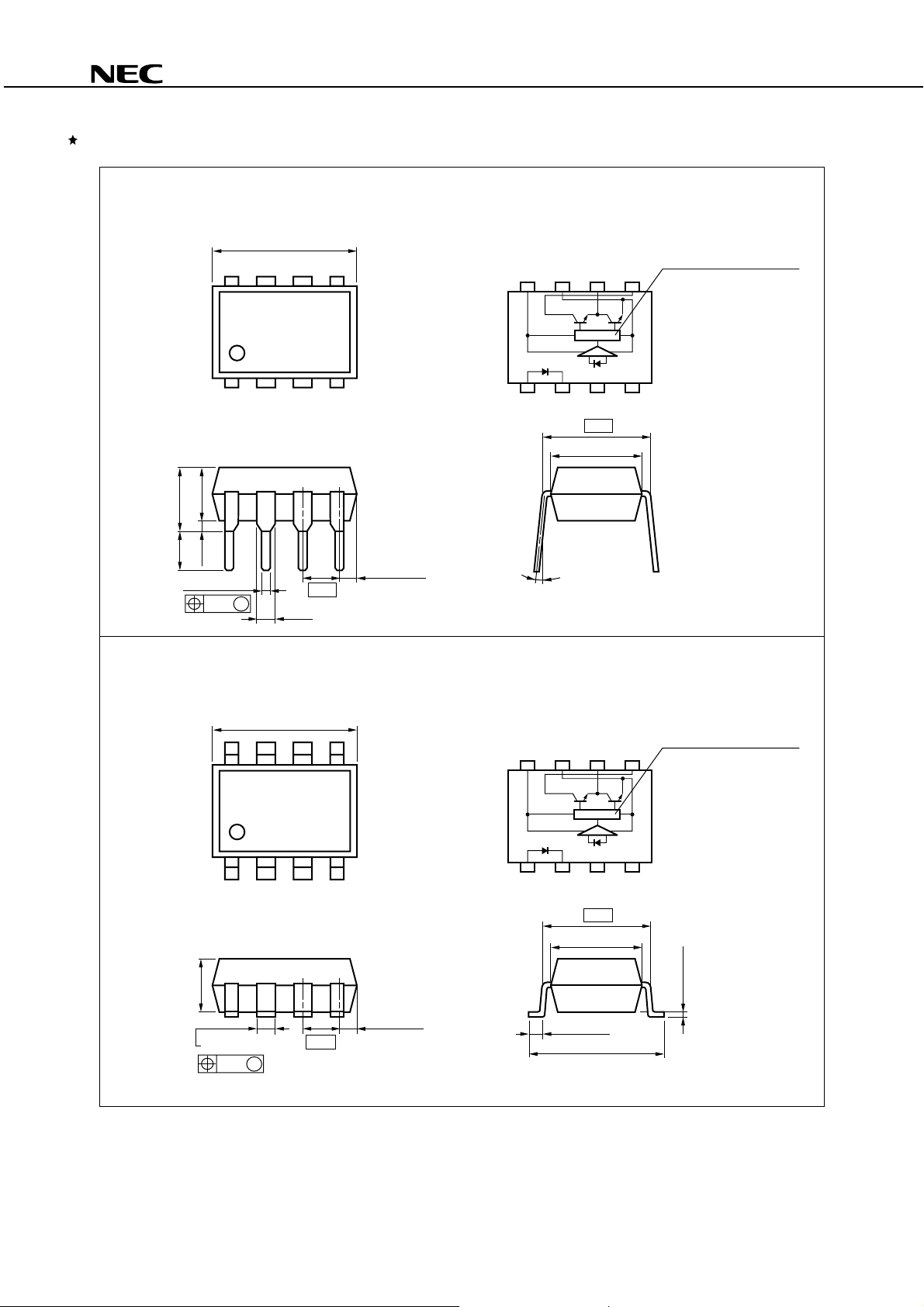
PACKAGE DIMENSIONS (in millimeters)
PS9634,PS9634L
PS9634
3.8 MAX.
4.55 MAX.
0.65
2.8 MIN.
0.50±0.10
0.25 M
10.16 MAX.
1.34
2.54
1.27 MAX.
PS9634L
TOP VIEW
8765
Tr.1 Tr.2
1234
7.62
6.5±0.5
0 to 15˚
Signal processing circuit
1. Anode
2. Cathode
3. NC
4. NC
5. Output (O1)
6. Output (O2)
7. GND
8. V
CC
3.8 MAX.
1.34±0.10
0.25 M
10.16 MAX.
2.54
1.27 MAX.
TOP VIEW
8765
Tr.1 Tr.2
1234
7.62
6.5±0.5
0.9±0.25
9.60±0.4
Signal processing circuit
1. Anode
2. Cathode
3. NC
4. NC
5. Output (O1)
6. Output (O2)
7. GND
CC
8. V
0.05 to 0.2
2
Page 3
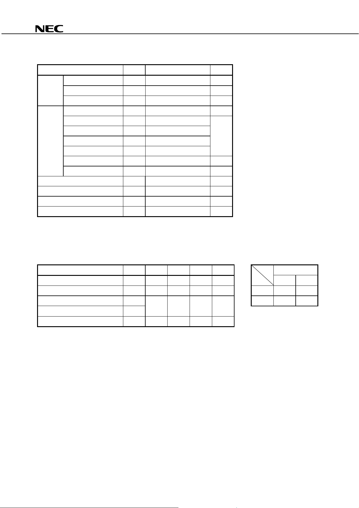
ABSOLUTE MAXIMUM RATINGS (TA = 25 °°°°C, unless otherwise specified)
Parameter Symbol Ratings Unit
PS9634,PS9634L
I
O1P
O2P
F
R
FM
CC
O1
O2
O1
O
30 mA
6.0 V
1A
18 V
0.5 A
1.0
0.8
2.0
18 V
500 mW
BV 5 000 Vr.m.s.
T
A
stg
550 mW
−
20 to +80
−
55 to +150
°
C
°
C
Diode Forward Current (DC) I
Reverse Voltage V
Peak Forward Current
*1
Detector Supply Voltage V
Output Current (O1) I
Peak Output Current (O1) I
Output Current (O2) I
Peak Output Current (O2) I
Output Voltage (O1) V
Power Dissipation P
Isolation Voltage
*2
Total Power Dissipat i on P
Operating Ambient Temperature T
Storage Temperature T
PW = 100
*1
AC voltage for 1 minute at TA = 25 °C, RH = 60 % between input and output
*2
s, Duty Cycle = 1 %
µ
RECOMMENDED OPERATING CONDITIONS TRUTH TABLE
Parameter Symbol MIN. TYP. MAX. Unit LED
Input On Current I
Supply Voltage V
Output Current (O1) I
Output Current (O2) I
Operating Ambient Temperature T
FLH
O1
O2
6 8 10 mA ON OFF
CC
5.4 15 V Tr. 1 ON OFF
0.1 0.2 0.3 A Tr. 2 OFF ON
A
02550
°
C
3
Page 4
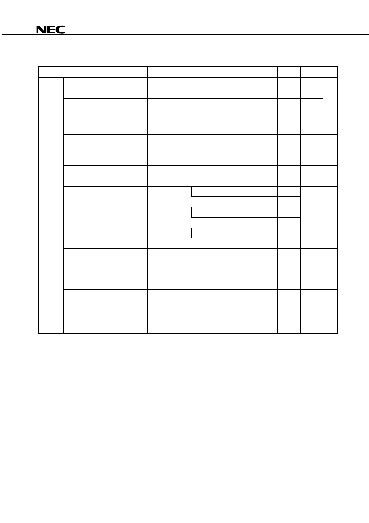
PS9634,PS9634L
ELECTRICAL CHARACTERISTICS (TA = −−−−20 to +80 °°°°C, unless otherwise specified)
Parameter Symbol Conditions MIN. TYP. MAX. Unit Fig.
Diode Forward Voltage V
Reverse Current I
Terminal Capacitance C
Detector Supply Voltage V
Low Level Output Voltage
V
(O1)
High Level Output Voltage
V
(O2)
Low Level Output Voltage
V
(O2)
Leakage Current (O1) I
Leakage Current (O2) I
High Level Supply Current I
Low Level Supply Current I
Coupled Input On Current (L → H) I
Isolation Resistance R
Propagation Delay Time
(L → H)
Propagation Delay Time
(H → L)
Instantaneous Common
CM
Mode Rejection Voltage
(Output: High)
Instantaneous Common
CM
Mode Rejection Voltage
(Output: Low)
F
IF = 5 mA, TA = 25 °C1.11.4V
R
VR = 5 V, TA = 25 °C5
t
V = 0 V, f = 1.0 MHz, TA = 25 °C30pF
CC
VCC = 6 V, IO1 = 0.4 A, RL2 = 10 Ω,
O1L
F
= 5 mA
I
O2H
VCC = 6 V, IO2 = −0.4 A, IF = 5 mA 4.5 5.0 V 2
O2L
VCC = 6 V, IO2 = 0.5 A, IF = 0 mA 0.25 0.40 V
O1L
VCC = 13 V, IF = 0 mA 100
O2L
VCC = 13 V, IF = 5 mA 100
CCH
CC
V
= 6 V, IF = 5 mA 16
CCL
CC
V
= 6 V, IF = 0 mA 22
FLH
VCC = 6 V, RL1 = 5 Ω, RL2 = 10
I-O
RH = 40 to 60 %, TA = 25 °C10
VCC = 6 V, IF = 5 mA, TA = 25 °C
PLH
t
t
PHL
L1
= 5 Ω, RL2 = 10
R
TA = 25 °C, VCM = 600 V (peak),
H
F
= 5 mA, RL1 = 470 Ω, RL2 = 1 k
I
∆
V02H = 2 V
TA = 25 °C, VCM = 600 V (peak),
L
F
= 0 mA, RL1 = 470 Ω, RL2 = 1 k
I
∆
V02L = 0.5 V
TA = 25 °C812mA
TA = 25 °C1518mA
TA = 25 °C 0.3 1.5 3.0 mA 5
Ω
Ω
5.4 15 V
0.25 0.40 V 1
0.2 5.0
11
35
−
1 000 V/
Ω,
1 000 V/
Ω,
µ
A
µ
A3
µ
A4
Ω
µ
s6
µ
s7
µ
s
4
Page 5

MEASUREMENT CIRCUITS FOR ELECTRICAL CHARACTERISTICS
PS9634,PS9634L
Fig. 1 V
I
F
1
2
O1L
I
F
8
V
CC
7
1
2
Fig. 4 I
8
7
O2L
V
CC
RL2 = 10 Ω
3
4
I
F
1
2
3
4
6
5
Fig. 2 V
8
7
6
5
O2H
–
V
O1L
V
+
I
O1
IF variable
V
CC
–
I
O2H
O2
V
V
+
3
4
1
2
3
4
6
5
Fig. 5 I
8
7
6
5
FLH
V
A
I
O2L
V
CC
–
R
L2
O2
V
= 10 Ω
+
6 V
R
L1
= 5 Ω
Fig. 3 I
I
F
1
2
3
4
I
F
SW
1
2
3
4
O1L
(t
r
, tf = 0.01 s)
V
8
V
CC
7
51 Ω
I
6
O1L
A
µ
IN
1
2
3
4
5
Fig. 7 CMH, CM
L
Fig. 6 t
8
7
6
5
PLH
, t
RL1 = 5 Ω
PHL
V
CC
RL2 = 10 Ω
V
OUT
V
V
t
PLH
IN
OUT
50 %
50 %
t
PHL
8
600 V
GND
CMH (IF = 5 mA)
2 V
L
CM
(IF = 0 mA)
7
6
5
RL1 = 470 Ω
R
L2
V
V
CC
= 1 kΩ
O2
V
CM
V
O2
0.5 V
+–
V
CM
5
Page 6

TYPICAL CHARACTERISTICS (TA = 25 °°°°C, unless otherwise specified)
PS9634,PS9634L
MAXIMUM FORWARD CURRENT vs.
AMBIENT TEMPERATURE
40
(mA)
F
30
20
10
Maximum Forward Current I
0
25 50 75 100
Ambient Temperature TA (˚C)
TOTAL POWER DISSIPATION vs.
AMBIENT TEMPERATURE
600
550
500
(mW)
T
400
300
POWER DISSIPATION vs.
AMBIENT TEMPERATURE
600
500
(mW)
O
400
300
200
Power Dissipation P
100
80
0
25 50 75 100
Ambient Temperature TA (˚C)
80
FORWARD CURRENT vs.
FORWARD VOLTAGE
100
TA = +100 ˚C
+75 ˚C
10
(mA)
F
1
+50 ˚C
+25 ˚C
0 ˚C
–25 ˚C
–55 ˚C
200
100
Total Power Dissipation P
0
25 50 75 100
Ambient Temperature TA (˚C)
80
NORMALIZED INPUT ON CURRENT vs.
SUPPLY VOLTAGE
1.5
VCC = 6 V
FLH
1.0
0.5
Normalized Input On Current I
0.0
28 164126101418
Supply Voltage VCC (V)
0.1
Forward Current I
0.01
0.8 1.0 1.4 1.60.6 1.2
Forward Voltage VF (V)
NORMALIZED INPUT ON CURRENT vs.
AMBIENT TEMPERATURE
1.3
Normalized to 1.0
A
= 25 ˚C,
at T
FLH
Normalized Input On Current I
CC
= 6 V
V
1.2
1.1
1.0
0.9
0.8
–20 20 60 80040
Ambient Temperature TA (˚C)
6
Page 7

PS9634,PS9634L
HIGH LEVEL SUPPLY CURRENT vs.
SUPPLY VOLTAGE
15
(mA)
CCH
T
10
5
High Level Supply Current I
0
810 14 1846
12
Supply Voltage VCC (V)
LOW LEVEL OUTPUT VOLTAGE (O1)
vs. OUTPUT CURRENT (O1)
0
10
(V)
O1L
–1
10
= –20 ˚C
A
+25 ˚C
+80 ˚C
16
VCC = 6 V
LOW LEVEL SUPPLY CURRENT vs.
SUPPLY VOLTAGE
22.5
= –20 ˚C
A
20.0
(mA)
CCL
T
+25 ˚C
17.5
+80 ˚C
15.0
12.5
10.0
Low Level Supply Current I
7.5
41216186 8 10 14
Supply Voltege VCC (V)
LOW LEVEL OUTPUT VOLTAGE (O1)
vs. AMBIENT TEMPERATURE
0.35
V
CC
(V)
O1L
0.30
0.25
0.20
= 6 V
IO1 = 0.5 A
0.3 A
–2
10
–3
Low Level Output Voltage (O1) V
10
10
–2
10
–1
Output Current (O1) IO1 (A)
LOW LEVEL OUTPUT VOLTAGE (O2)
vs. OUTPUT CURRENT (O2)
0
10
(V)
O2L
–1
10
–2
10
–3
Low Level Output Voltage (O2) V
10
–2
10
Output Current (O2) IO2 (A)
10
–1
VCC = 6 V
10
10
0.15
0.10
0.1 A
0.05
Low Level Output Voltage (O1) V
0
0.00
020 6080–20 40
Ambient Temperature TA (˚C)
LOW LEVEL OUTPUT VOLTAGE (O2)
vs. AMBIENT TEMPERATURE
0.5
V
CC
(V)
O2L
0.4
0.3
0.2
0.1
Low Level Output Voltage (O2) V
0
0.0
= 6 V
IO2 = 0.6 A
0.4 A
0.1 A
0406080–20 20
Ambient Temperature TA (˚C)
7
Page 8

PS9634,PS9634L
HIGH LEVEL OUTPUT VOLTAGE (O2)
vs. OUTPUT CURRENT (O2)
5.5
(V)
O2H
5.0
4.5
High Level Output Voltage (O2) V
4.0
–0.1 –0.4 –0.60.0 –0.2 –0.3 –0.5
Output Current (O2) IO2 (A)
PROPAGATION DELAY TIME vs.
FORWARD CURRENT
5
µ
( s)
PHL
/t
PLH
t
PLH
t
PHL
4
VCC = 6 V,
R
R
TA = +80 ˚C
VCC = 6 V
L1
= 5 Ω,
L2
= 10 Ω
HIGH LEVEL OUTPUT VOLTAGE (O2)
vs. AMBIENT TEMPERATURE
5.3
(V)
O2H
5.2
5.1
V
CC
= 6 V
= –0.1 A
O2
I
–0.4 A
5.0
–0.6A
4.9
4.8
4.7
4.6
High Level Output Voltage (O2) V
4.5
–20 40 80020 60
Ambient Temperature TA (˚C)
PROPAGATION DELAY TIME vs.
AMBIENT TEMPERATURE
5.0
µ
( s)
4.5
PHL
/t
PLH
4.0
3.5
VCC = 6 V, IF = 5 mA,
L1
= 5 Ω, RL2 = 10 Ω
R
t
PHL
t
PLH
3
–20 ˚C
Propagation Delay Time t
2
520300101525
Forward Current IF (mA)
SAFE OPERATING AREA (Tr.1)
10
5
(A)
O2
IO2 MAX. (Pulse)
2
1
IO2 MAX. (DC)
0.5
Output Current (O2) I
0.2
0.1
*1 One pulse
*2 On the epoxy board
DC (T
A
= 80 ˚C)
15 300.3 2 3 100.5 20
Output Voltage (O2) VO2 (V)
DC
3.0
+25 ˚C
2.5
Propagation Delay Time t
2.0
080–20 20 40 60
Ambient Temperature TA (˚C)
1 ms
10 ms
100 ms
1 s
*1
*2
*2
*1
*1
*1
MAX.
CC
V
8
Remark
The measurement of TYPICAL CHARACTERISTICS are only for reference, not guaranteed.
Page 9

TAPING SPECIFICATIONS (in millimeters)
Outline and Dimensions (Tape)
2.0±0.1
4.0±0.1
1.55±0.1
12.0±0.1
Tape Direction
1.55±0.1
10.4±0.1
1.75±0.1
7.5±0.1
16.0±0.3
PS9634,PS9634L
4.3±0.2
10.3±0.1
0.3
PS9634L-E3 PS9634L-E4
Outline and Dimensions (Reel)
R 1.0
2.0±0.5
13.0±0.5
φ
φ
21.0±0.8
330
φ
80.0±5.0
φ
Packing: 1 000 pcs/reel
16.4
+2.0
–0.0
9
Page 10

PS9634,PS9634L
RECOMMENDED SOLDERING CONDITIONS
(1) Infrared reflow soldering
• Peak reflow temperature 235 °C (package surface temperature)
• Time of temperature higher than 210 °C 30 seconds or less
• Number of reflows Three
• Flux Rosin flux containing small amount of chlorine (The flux with a
maximum chlorine content of 0.2 Wt % is recommended.)
Recommended Temperature Profile of Infrared Reflow
(heating)
to 10 s
235 ˚C (peak temperature)
210 ˚C
to 30 s
120 to 160 ˚C
60 to 90 s
(preheating)
Package Surface Temperature T (˚C)
Time (s)
Caution Please avoid to removed the residual flux by water after the first reflow processes.
Peak temperature 235 ˚C or below
(2) Dip soldering
• Temperature 260 °C or below (molten solder temperature)
• Time 10 seconds or less
• Number of times One
• Flux Rosin flux containing small amount of chlorine (The flux with a maximum chlorine content of
0.2 Wt % is recommended.)
10
Page 11

PS9634,PS9634L
APPLICATION EXAMPLE OF PHOTOCOUPLER (TO POWER TRANSISTOR MODULE)
V
CC
PS9634, PS9634L
TTL or the like
Input
V
IN
V
CC
1
2
8
7
Load
+
3
4
6
I
O
5
Power transistor module
V
IN
0
t
I
O
0
I
O1
O2P
I
t
11
Page 12

PS9634,PS9634L
CAUTION
Within this device there exists GaAs (Gallium Arsenide) material which is a
harmful substance if ingested. Please do not under any circumstances break the
hermetic seal.
No part of this document may be copied or reproduced in any form or by any means without the prior written
consent of NEC Corporation. NEC Corporation assumes no responsibility for any errors which may appear in this
document.
NEC Corporation does not assume any liability for infringement of patents, copyrights or other intellectual
property rights of third parties by or arising from use of a device described herein or any other liability arising
from use of such device. No license, either express, implied or otherwise, is granted under any patents,
copyrights or other intellectual property rights of NEC Corporation or others.
While NEC Corporation has been making continuous effort to enhance the reliability of its semiconductor devices,
the possibility of defects cannot be eliminated entirely. To minimize risks of damage or injury to persons or
property arising from a defect in an NEC semiconductor device, customers must incorporate sufficient safety
measures in its design, such as redundancy, fire-containment, and anti-failure features.
NEC devices are classified into the following three quality grades:
"Standard", "Special", and "Specific". The Specific quality grade applies only to devices developed based on
a customer designated "quality assurance program" for a specific application. The recommended applications
of a device depend on its quality grade, as indicated below. Customers must check the quality grade of each
device before using it in a particular application.
Standard: Computers, office equipment, communications equipment, test and measurement equipment,
audio and visual equipment, home electronic appliances, machine tools, personal electronic
equipment and industrial robots
Special: Transportation equipment (automobiles, trains, ships, etc.), traffic control systems, anti-disaster
systems, anti-crime systems, safety equipment and medical equipment (not specifically designed
for life support)
Specific: Aircrafts, aerospace equipment, submersible repeaters, nuclear reactor control systems, life
support systems or medical equipment for life support, etc.
The quality grade of NEC devices is "Standard" unless otherwise specified in NEC's Data Sheets or Data Books.
If customers intend to use NEC devices for applications other than those specified for Standard quality grade,
they should contact an NEC sales representative in advance.
Anti-radioactive design is not implemented in this product.
M4 96. 5
 Loading...